734 IEEE TRANSACTIONS ON ELECTRON DEVICES, VOL. 41, NO. 5, MAY 1994
New
Observation and the Modeling
of
Gate
and Drain Currents in Off-state
P-MOSFET's
Ming-Jer
Chen, Member, ZEEE,Kum-Chang
Chao, and Chia-Hsiang ChenAbstract-The work reports new observations concerning the gate and drain currents measured at off-state conditions in buried-type p-channel LDD MOSFET devices. Detailed inves- tigation of the observed phenomena reveals that 1) the drain current can be separated into two distinct components: band-to- band tunneling in the gate-to-drain overlap region and collection of holes generated via impact ionization by electrons inside the oxide; and 2) the gate current can be separated into two distinct components: the hot electron injection into the oxide and the Fowler-Nordheim electron tunneling through the oxide. At low negative drain voltage, the dominant component of the drain current is the hole generation inside the oxide. At high negative drain voltage, the drain current is essentially due to band-to-band tunneling, and it is correlated with the hot-electron injection- induced gate current.
I. INTRODUCTION
HE gate and drain currents in off-state MOS devices have
T
recently been studied extensively [I]-[ 151. An under- standing of the mechanisms responsible for these currents as well as their control is very important to device application and to reliability study. In the work of [ 11-[ 141, the drain leakage current has been judged to be dominated by one or more of the mechanisms occumng in the gate-to-drain overlap region: the band-to-band tunneling [ 11-13], [9]-[ 141, the trap-assisted tunneling [5], and the surface diffusion-limited transport [8]; and the gate current has been interpreted by one or more of the following mechanisms: the hot-camer injection into the oxide[4], [6], [7], [12] and the electron Fowler-Nordheim (F-N) tunneling through the oxide [4], [6], [ l l ] . In our previous work [15], we measured gate and drain currents in off-state 180 8, gate oxide buried-type LDD p-MOSFET device. It
tumed out that the gate current is dominated by the F-N tunneling of electrons from the surface beneath the gate and the holes generated via impact ionization by electrons within the oxide constitute the drain leakage current. However, the ability to accurately model the drain current component due to hole generation inside the oxide has not been established in [15]. Since the measurement condition was limited to low negative drain voltages [ 151, no other currents due to the band- to-band tunneling and hot-carrier injection have been found in Manuscript received October 22, 1993; revised December 22, 1993. The review of this paper was arranged by Associate Editor D. A. Antoniadis. This work was supported by the National Science Council under Contract NSC 82-0404-E-009-232/246.
M. J. Chen and K. C. Chao are with Department of Electronics Engineering and Institute of Electronics, National Chiao-Tung University, Hsin-Chu, Taiwan 300, Republic of China.
C. H. Chen is with Taiwan Semiconductor Manufacturing Company, Ltd., Hsin-Chu, Taiwan 300, Republic of China.
IEEE Log Number 9400819.
the drain and gate, respectively. However, as we modify this measurement condition by slightly increasing negatively the drain voltage, a dramatically large change in I-V characteristics is observed, which is not reported in [15]. Such experimental observations have been found to be reproducible for devices with gate oxide thickness of 106-185
A.
An investigation of these new I-V characteristics has revealed that 1) both theband-to-band tunneling and the holes generated inside the oxide simultaneously contribute to the drain leakage current; and 2) both the hot-electron injection and the electron F-N
tunneling simultaneously contribute to the gate current. In this paper, we will report these observation results along with the detailed analysis and modeling.
11. EXPERIMENTAL OBSERVATION
The work is based on the nf-gate buried-type p-channel LDD MOSFET devices having three gate oxide thicknesses of 106, 146, and 185
A.
The corresponding gate width to length ratios are 50 pm/0.7 pm, 100 p d l . 0 pm, and 100 pm/1.5 pm, respectively. The devices were fabricated by a 0.6-pm twin-well polysilicon CMOS process. The starting material was p-type<
100>-oriented wafers with resistivityof 8-12 0-cm. Phosphorus (6.0 x 101'cm-', 150 KeV) was implanted to form the n-well region. BFz (2.6 x
lo1'
cm-',70 KeV) was used as the threshold voltage implant. The gate oxide was grown in dry 0 2 at 920°C. After n+ gate polysilicon was formed, BFz (1.0 x 1013 cm-', 45" angle rotating, 50 KeV) was implanted to form the low-doped drain region and BFz (3.0 x 10¹⁵c1n-2, 70 KeV) was implanted to form the highly doped drain region. The junction depth and surface doping concentration of the low-doped drain have been determined to be about 0.25 pm and 3.0 x 10l8 cmP3, respectively. The threshold voltage values of the samples are around -0.7 V.
We have found that the experimental observations to be demonstrated later are independent of the gate oxide thickness. Therefore, unless stated otherwise, only the measurement results from the 146
A
gate oxide case are presented. With the source floating and the n-well grounded, each structure with the assigned drain terminal condition has been characterized as shown schematically in Fig. 1. Under this condition, the gate and drain currents have been measured as function of gate voltage ranging from 0 to 20 V. Unless stated otherwise, the measurement results presented in this paper have been performed at room temperature of 27OC. The drain and gate current measurement results for V, = 0, - 3 , - 5 , and -7 V are shown in Fig. 2 and 3, respectively. The measured_ _
CHEN ef al.: NEW OBSERVATION AND THE MODELING OF GATE AND DRAIN CURRENTS 135
H
N-well
Fig. 1.
device for measuring the off-state gate and drain currents.
The terminal connection condition of the buried-type p-MOSFET
gate current versus gate voltage for the drain floated is also depicted in Fig. 3 . For VD = 0 and -3 V, 1) both the gate and drain currents are independent of drain voltage; and 2) the gate current 1, is greater than the drain current I D with
an I G / I D ratio of about 1 x
lo2
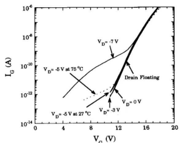
to 2 x lo3. Moreover, the gate current is not affected when the drain is floated. These observation results at high gate voltage are indeed in goodagreement with those reported in a 180 8, gate oxide p- MOSFET device fabricated by the 0.8 pm polycide CMOS process [15]. However, as we increase negatively the drain voltage from -3 V to -5 V, a dramatically large change in I-V characteristics occurs. We can observe that a significant drain current at VD = -5 V appears in a wide range of VG
between 4 and 17 V while in most of this range (i.e., 4 V
<
Vc
<
1 3 V ) no data of interest except the measurement noise or conventional thermal generation current can be detected in the drain for VD = 0 and -3 V. Only for high gate voltage greater than about 17 V as shown in Fig. 2, the drain current is becoming independent of VD ranging from0 to -5 V. Since the measurement noise disturbs the low current regime in Fig. 3 , no change in the gate current can be accurately detected. This difficulty can be overcome by increasing the measurement temperature. The measurement results of the drain and gate currents at VD = -5 V for two different temperatures of 27 and 75°C are shown in Fig. 2 and 3, respectively. The measured drain current shown in Fig. 2 exhibits a positive temperature coefficient, i.e., the drain current increases as the temperature increases. From Fig. 3 we can confidently determine a detectable range of VG
between 7-11 V for VD = -5 V at 75"C, where the gate current can be recognized to be significantly different from the measurement noise or conventional thermal generation as obtained at room temperature. Moreover, this new observation can be demonstrated more clearly by simply changing VD from -5 V to -7 V. The corresponding measurement results are shown in Figs. 2 and 3, from which it can be clearly seen that the drain current exponentially increases with increasing VD.
A dramatic change in the IG for VD = -7 V has also been observed for a wide range of VG between 4 and 14 V while for VG greater than about 14 V the gate current is becoming
independent of drain voltage.
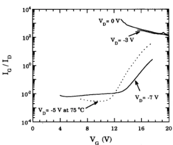
The ratio of the measured gate to drain current is shown in
Fig. 4 for VD = 0, -3, and -7 V as well as for V, = -5 V at 75°C. From Fig. 4 we can observe that the gate to drain
h
s
n U 108 10-10 10-'2 1 ° jFig. 2. The measured drain current versus gate voltage characteristics for four different drain voltages of 0, -3. -5. and -7 V. The drain current versus gate voltage characteristic obtained at 75' C for Vj = -5 V is also shown for comparison. The current components due to the measurement noise and conventional thermal generation have been subtracted for clarity. The gate oxide thickness is 146 A.
vD= vat n 'c 'D= -3v
" " "4 " " ' 18 ' ' '12 1 ~ ~16 ' 1 20
VG 0
Fig. 3. The measured gate current versus gate voltage characteristics corre- sponding to Fig. 2. The gate current versus gate voltage characteristic for the drain floated is also shown.
1 x 10' and 2 x
lo3
and decreases with increasing gate voltage. It can be seen from Fig. 4 that for VD = -7 V there exists a wide VG range about between 4 and 14 V where the gate to drain current ratio is almost a constant of about 1 x l o p 2 ; and from VG = 14 V this ratio starts to increase exponentially with increasing the gate voltage. The case of VD = -5 V at 75°C is similar to that of VD = -7 V but with two significant differences: 1) there is a relatively small VG range of about7-1 1 V where the gate to drain current ratio can be reasonably considered constant; and 2) this constant is about 3 x
considerably smaller than that at VD = -7 V.
111. F-N TUNNELING AND HOLE GENERATION The measurement results mentioned above show that for small values of VD (i.e., VD = 0-3 V) 1) the drain current current ratio corresponding to VD = 0 and -3 V ranges from is less than the gate current by about two to three orders
736 IEEE TRANSACTIONS ON ELECTRON DEVICES, VOL. 41, NO. 5, MAY 1994 the oxide is suggested to be the origin of our measured drain hole current. Indeed, in Fig. 6 the drain current density J D
is independent of the bias VD, indicating the role of the drain only for collecting the holes generated. Based on the published impact ionization coefficient model [ 191, [20], the drain current
component 1 0 1 by collecting the holes generated inside the
oxide has been calculated [ 161:
101 = a, exp (-H/Eox)(Tox - T t ) h ( 2 ) where the parameter values of a , = 3.3 x 106cm-' and
H = 80 MV/cm as cited in [19], [20] are used.
Tt (=
+ B / q E o x4 a 12 16 2o for barrier height $JB = 3.2 eV) is the tunneling distance and
0
the value of (Tax - T,) is the effective length for impact
ionization. By substituting the experimental data in Fig. 5
Fig. 4. The gate to drain current ratio as function of gate voltage for
tb
= 0 , - 3 . and -7 V as well as for tb = -5 V at 75' C. The drain current is from Fig. 2 and the gate current is from Fig. 3.into ( 2 ) , the calculated results are shown in Fig. 6. It can be observed from Fig. 6 that without any parameter adjusting, the agreement with experimental I-V data for three different of magnitude; 2 ) both the gate and drain currents are in-
dependent of drain voltage; and 3) the gate current is not affected by making the drain floated. Such characteristics appearing primarily at high positive gate voltage can be explained satisfactorily based on the formation of the surface n+ inversion layer due to the punchthrough of the buried channel to the underlying shallow p-n junction [15]. The electron F-N tunneling from this layer and the collection of the
oxide thicknesses is very good.
The phenomenon of oxide breakdown has been noted in Fig. 6. Here we demonstrate the correlation of the hole generation to oxide breakdown. Based on the hole-trapping- induced breakdown model [ 161, [ 191, oxide breakdown occurs when the density of trapped holes reaches some critical value
Q2
Q; = 8
l""
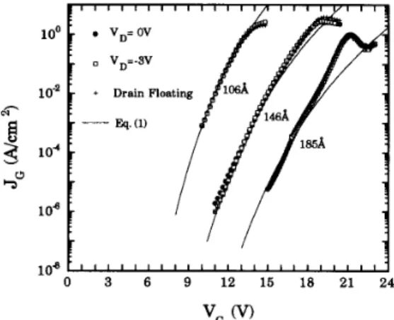
JDdt (3)holes generated via impact ionization by electrons inside the oxide have been judged experimentally to contribute the gate and drain currents, respectively [15], [16]. To further judge the validity of this interpretation, we measured gate and drain currents for three different oxide thicknesses (Figs. 5 and 6).
where 8 is the trapping efficiency and tbd is the time necessary
for breakdown. To evaluate (3) more easily, a ramp voltage for
VG with the ramp rate R (volts per second) has been assumed. As a result, (3) can be written as
Fig. 6 also labels the values of gate voltage for instant oxide
breakdown. The F-N tunneling current component 1 ~ 1 has been calculated using the expression [ 171:
where AG is the oxide area, To, is the oxide thickness, and
Eo,
(II VG/T,, for large VG values) is the oxide field strength.The values of two constants a1 = 1 . 7 6 ~ lop6 A/V2 and a2 =
245.5 MV/cm have been obtained by fitting the measured gate current in Fig. 5. These fitted parameters values have been
found to be comparable with those of a1 = 2.3 x lop6 A/V2 and a2 = 238.5 MV/cm as cited in [18]. The calculated results based on our fitted parameter values have been supported by the experimental data in Fig. 5. From Fig. 5 it can be
observed that except at the high current level where the effects of the trapped charges dominate, the agreement with experimental I-V data for three different oxide thicknesses has been simultaneously achieved.
According to the work [15], [16], not only the holes generated inside the high-field oxide are linked to the electron tunneling from the n+ inversion layer surface, but also both are function of only the oxide field. Therefore, the mechanism of the holes generated via impact ionization by electrons within
(4)
where VGB is the gate voltage for instant breakdown. Based
on the experimental data in Fig. 6, the values of QLR/8 have been calculated using (4) to be 1.03 x 1.44 x
and 1.05 x 10W2A . V/cm2 for
Tox
= 106, 146, and 185A,
respectively. The close agreement between these calculated values supports the hole generation mechanism proposed above for the measured drain current.I v . ANALYSIS AND DISCUSSION
As we increase negatively the drain voltage from V, = -3 V by a small value, a significant change in I-V characteristics occurs as shown in Fig. 2 and 3 for VD = -5 and -7 V. We can attribute the increased drain current to one or more
of the mechanisms: the band-to-band tunneling [ 11-[3], the trap-assisted tunneling [ 5 ] , and the surface diffusion-limited
transport [8]. We favor band-to-band tunneling, by considering
several data: 1) the associated drain voltage magnitude (i.e.,
5 V and 7 V) is less than our measured drain breakdown
voltage of about 13 V; and 2 ) the drain current has a positive temperature coefficient as shown in Fig. 2. To model the drain
CHEN et al.: NEW OBSERVATION AND THE MODELING OF GATE AND DRAIN CURRENTS 737 ' I 1 1 " " 1 1 1 ' 1 1 1 1 1 1 1 ' 1 1 1 1 1 0 3 6 9 12 15 18 21 24 ' G
*
Fig. 5. The gate current density .I<; versus gate voltage 1
>;
measured under different connection conditions of the drain terminal for three different oxide thicknesses. The calculated results using ( 1 ) are also shown for comparison.current component 102 for VD = -7 V, an analytic model of band-to-band tunneling is considered [ 11-[3]:
( 5 )
where [?I and /?2 are two fitting parameters and E,i is the
effective field strength. The deep depletion approximation has been utilized for the Esi:
I D 2 =
P1
E s i exp (-,&'/Est)Ki
= (vG - vD)+
9 q ~ ~ 4 ~ , 2 , / ~ , , - ((vG - VD+
gqN.4T,2/Esi)' - (vG - vD)*)~" (6) 1 Esi =2
(2qN.4Ki/Esi)1/2 (7)where Vsi is the silicon surface band-bending voltage, N A is the effective drain doping concentration, and is the silicon permittivity. Note that a linear distribution of the vertical electric field as recently reported in [14] has been utilized for (7). Based on ( 3 4 7 ) the values of = 2.842 x
lo-'
A-cm/V and
,&
= 15.16 MV/cm have been properly extracted for VD = -7 V. The corresponding calculated drain current is shown in Fig. 7 where the experimental data forVD
= -7 V are also shown for comparison. From Fig. 7 we can observe that a reasonable agreement with experimental data has been achieved, indicating the role of the band-to-band tunneling in this case.A significant gate current for
VD
= -7 V has been detected over theVG
range from about 4-14 V. This range of Vc is narrowed to between about 7-11 V for VD = -5 V at 75°C. In these ranges the gate current cannot be accounted for simply by the F-N tunneling mechanism. We attribute this current to the hot-electron injection into the oxide under the influence of the surface lateral field in the gate-drain overlap region. The reasons are as follows: 1) for theVD
fixed to -7 V, the gate to drain current ratio is nearly a constant over a wideV,
range from 4 to 14 V as shown in Fig. 4, indicating the role of the surface lateral field for this ratio; 2) this ratio for VD = -5 V at 75°C is also a constant over a relatively smallVG
range as shown in Fig. 4; and 3) over the sameV,
range of betweenI I I I I I ' I I I I I I I 1 I
Fig. 6. The drain current density J D versus gate voltage 1;; measured under different connection conditions of the drain terminal for three different oxide thicknesses. The gate voltage values for instant oxide breakdown are labeled. The calculated results using (2) with the measured .Jc; in Fig. 5 as input parameter are also shown for comparison.
h
Fig. 7. The calculated drain current as function of gate voltage by the impact ionization generation expression (2) for 1; = 0 and -3 V, and by the band-to-band tunneling expression (5) for 1b = -7 V. The associated experimental data are deduced from Fig. 2 for comparison.
7 and 1 1 V the gate to drain current ratio for VD = -7 V
is larger than that for
VD
= -5 V at 75°C as shown in Fig. 4, in agreement with the lucky electron concept [21], [22] since the lateral field decreases as the reverse-bias drain voltage magnitude decreases. The corresponding gate current component I G ~ can be modeled by an empirical expression based on the lucky electron model [21], [22]:IG2 = 1 7 1 0 2 (8)
where the coefficient 71 is a constant for a fixed VD. This
can be identified by noting from Fig. 4 that the ratio of the gate to drain current for
VD
= -7 V has a constant value of about 1 x lo-' overVG
= 4 to 14 V. To confirm the proposed interpretations, the calculated gate current using (8)with 71 = 1 x lo-' for
VD
= -7 V is shown in Fig. 8 along with the experimental data. The gate current calculated by summing (1) and (8), i.e., I , = I G ~+
1 ~ 2 , is also shown in Fig. 8 for comparison. From Fig. 8, we can observe that close738
Experiment Model I,. + I,.
... UT
1
“i
:
.;,
,
, , , I , , ;: I , , , , , ,{
:?- I,, 4 8 12 16 20 10’14~ .’Fig. 8. The calculated gate current as function of gate voltage by the F-N tunneling expression (1) for = 0 and -3 V, and by the hot-electron injection expression (8) with r] = 1 x IO-’ for 1 = -7 V. The associated experimental data are deduced from Fig. 3 for comparison. The superposition of the gate current components from (1) and (8) is also demonstrated.
agreements with experimental data have been achieved. Also we have found that for VG
<
14 V we have I G ~<<
I G ~ whileI G ~
>>
I G 2 for VG>
14v.
V. CONCLUSION
I-V characteristics in the gate and drain have been measured in the off-state buried-type p-MOSFET devices. Two drain current components are witnessed: band-to-band tunneling in the gate-drain overlap region and the collection of the holes generated inside the oxide. The gate current components are hot-electron injection into the oxide and the F-N electron tunneling through the oxide. The correlation between the drain current component due to the band-to-band tunneling and the gate current component due to the hot-electron injection has been successfully modeled. The gate current component due to the F-N tunneling has also been successfully correlated to the drain current component due to the hole generation in oxide without adjusting any parameter.
ACKNOWLEDGMENT
The authors would like to thank the reviewers for helpful comments and suggestions.
REFERENCES
J. Chen, T. Y. Chan, I. C. Chen, P. K. KO, and C. Hu, “Subbreakdown drain leakage current in MOSFET,” IEEE Electron Device Lefr.. vol. 8, pp. 515-517, 1987.
C. Chang and J. Lien, “Comer-field induced drain leakage in thin oxide MOSFETs,” IEDM Tech. Dig., pp. 714-717, 1987.
T. Y. Chan, J. Chen, P. K. KO, and C. Hu, “The impact of gate-induced drain leakage current on MOSFET scaling,” 1987 IEDM Tech. Dig.. pp. 718-721, 1987.
C. Chang, S. Haddad, B. Swaminathan, and J. Lien, “Drain-avalanche and hole-trapping induced gate leakage in thin oxide MOS devices,”
IEEE Electron Device Left.. vol. 9, pp. 588-590, 1988.
1. C. Chen, C. W. Teng, D. J. Coleman, and A. Nishimura, “Interface- trap enhanced gate-induced leakage current in MOSFET,” IEEE Elecrron
Device Left., vol. IO, pp. 2 1 6 2 1 8 , 1989.
J. Chen, T. Y. Chan, P. K. KO, and C. Hu, “Gate current in off-state MOSFET,” IEEE Electron Device Lett.. vol. 10, pp. 203-205, 1989.
IEEE TRANSACTIONS ON ELECTRON DEVICES, VOL. 41, NO. 5, MAY 1994
Y. Igura, H. Matsuoka, and E. Takeda, “New device degradation due to ‘cold’ camers created by band-to-band tunneling,” IEEE Electron
Deivce Left., vol. 10, pp. 227-229, 1989.
W. P. Noble, S. H. Voldman, and A. Bryant, “The effects of gate field on the leakage characteristics of heavily doped junctions,” IEEE Trans.
Electron Devices, vol. 36, pp. 72C726, 1989.
T. Endoh, R. Shirota, M. Momodomi, and F. Masuoka, “An accurate model of subbreakdown due to band-to-band tunneling and some applications,” IEEE Trans. Elecrron Devices. vol. 37, pp. 29C295, 1990.
M. J. Chen, “Effect of back-gate bias on tunneling leakage in a gated p+-n diode,” IEEE Elecfron Device Left., vol. 12, pp. 249-251, 1991. M. J. Chen, “New observation of gate current in off-state MOSFET,”
lEEE Trans. Elecrron Devices, vol. 38, pp. 21 18-2120, 1991.
I. C. Chen and C. W. Teng, “A quantitative physical model for the band-to-band tunneling-induced substrate hot electron injection in MOS devices,” IEEE Trans. Elecrron Devices, vol. 39, pp. 1646-1651, 1992. S. A. Parke, J. E. Moon, H. J. Wann, P. K. KO, and C. Hu, “Design for suppression of gate-induced drain leakage in LDD MOSFET’s using a quasi-two-dimensional analytical model,’’ IEEE Trans. Electron Devices, vol. 39, pp. 1694-1703, 1992.
H. J. Wann, P. K. KO, and C. Hu, “Gate-induced band-to-band tunneling leakage current in LDD MOSFETs,” in 1992 IEDM Tech. Dig., pp. 147- 1 SO.
M. J. Chen, K. C. Chao, T. H. Huang, and J. M. Tsaur, “Gate and drain currents in off-state buried-type p-channel LDD MOSFET’s,” IEEE
Electron Device Lett., vol. 13, pp. 6.54-657, 1992.
I. C. Chen, S. E. Holland, K. K. Young, C. Chang, and C. Hu, “Substrate hole current and oxide breakdown,” Appl. Phys. Lett., vol. 49, pp. 669-67 1, 1986.
M. Lenzilinger and E. H. Snow, “Fowler-Nordheim tunneling into thermally grown Si02,” J. Appl. Phys., vol. 40, pp. 278-283, 1969.
2. A. Weinberg, “On tunneling in metal-oxide-silicon structures,” J. Appl. Phys., vol. 53, pp. 5052-5056, 1982.
I. C. Chen, S. E. Holland, and C. Hu, “Electrical breakdown in thin gate and tunneling oxides,” lEEE J. Solid-state Circuits, vol. 20, pp. 333-342, 1985.
J. C. Lee, I. C. Chen, and C. Hu, “Modeling and characterization of gate oxide reliability,” IEEE Trans. Elecfron Devices, vol. 35, pp. 2268-2278, 1988.
T. H. Ning, C. M. Osbum, and H. N. Yu, “Emission probability of hot electron from silicon into silicon dioxide,” J. Appl. Phys., vol. 48, pp. 286293, 1977.
S. Tam, P. K. KO, and C. Hu, “Lucky-electron model of channel hot-electron injection MOSFET’s,” IEEE Trans. Electron Devices, vol. ED-31, pp. 1116-1125, 1984.
Ming-Jer Chen (S‘77-M‘86) was bom in Taiwan on April 1, 1954. He received the B.S. degree with highest honors from the National Cheng-Kung University in 1977, and the M.S. and Ph.D. degrees from the National Chiao-Tung University in 1979 and 1985, respectively, all in electrical engineering.
During 1979-1980, he worked for the Telecom- munication Laboratories, Taiwan, where he was responsible for the design and implementation of a multiprocessor distributed system. In 1985 he conducted postdoctoral research on CMOS latch- up at the National Chiao-Tung University. From 1986 to 1992 he was an Associate Professor at the National Chiao-Tung University. He is now a Professor in the Department of Electronics Engineering and the Institute of Electronics. Since 1988 he has cooperated with the Taiwan Semiconductor Manufacturing Company in the submicron device reliability program. His present research interests include submicron device reliability, subthreshold CMOS circuits, and special BiCMOS structures.
CHEN ~f al.: NEW OBSERVATION AND THE MODELING OF GATE AND DRAIN CURRENTS 139
Chia-Hsiang Chen received the B.S. degree in electrophysics and the M.S. degree in electro-optics from the National Chiao-Tung University, Taiwan, in 1981 and 1985, respectively.
In 1985, he worked on the GaAs MESFET pro- cessing at MRL/ITRI During 19861989, he was involved in the processing of an infrared detector based on both the InSb CID arrays and the HgCdTe
PV, PC arrays at CSIST, Taiwan In 1989, he joined the R&D department of TSMC and from then he has worked on the process development and device Kum-Chang Chao was born in Taiwan on October
18, 1965. In 1988 he received the B.S. degree in electncal engineenng from the National Chiao- Tung University, Hsin-chu, Taiwan. He IS currently working toward the Ph.D. degree in the Institute of Electronics, National Chiao-Tung University, Hsin- chu, Taiwan. His research interests include the mod- eling and reliability study of deep submicron CMOS devices
design. Now he is the manager of device engineering section, Technology Development Division, Taiwan Semiconductor Manufacturing Company, Ltd., Hsin-Chu, Taiwan.
![Fig. 8. The calculated gate current as function of gate voltage by the F-N tunneling expression (1) for = 0 and -3 V, and by the hot-electron injection expression (8) with r] = 1 x IO-’ for 1 = -7 V](https://thumb-ap.123doks.com/thumbv2/9libinfo/7690814.143334/5.927.139.428.90.333/calculated-current-function-tunneling-expression-electron-injection-expression.webp)
