國立交通大學
光電工程研究所
碩士學位論文
光子晶體面射型雷射特性之研究
Study of Characteristics of Photonic Crystal
Vertical Cavity Surface Emitting Lasers
研 究 生:許意偵
指導教授:王興宗 教授
郭浩中 教授
光子晶體面射型雷射特性之研究
Study of Characteristics of Photonic Crystal Vertical Cavity Surface
Emitting Lasers
研 究 生:許意偵 Student:I-Chen Hsu
指導教授:王興宗 Advisor:Shing-Chung Wang
郭浩中 Hao-Chung Kuo
國 立 交 通 大 學
光 電 工 程 研 究 所
碩 士 論 文
A ThesisSubmitted to Institute of Electronics College of Engineering National Chiao Tung University
in partial Fulfillment of the Requirements for the Degree of
Master
In Electro-Optical Engineering
July 2006
Hsinchu, Taiwan, Republic of China
誌謝
能夠順利的完成兩年的碩士生涯,要感謝的人很多。首先要感謝的是實驗室精神 領袖王興宗教授,在他的指導和教誨下,使我學習到很多專業的知識和做研究的態 度,而他那種對研究積極樂觀且永不放棄的精神,是我永遠學習的榜樣。此外我還 要感謝另一位指導老師郭浩中教授,有他的指導和提供專業的實務與經驗,加深了 我對專業領域的專業知識。此外我也要感謝盧廷昌老師的指導,他不時提醒我在研 究成果上的缺失和寶貴的建議,讓我的實驗內容可以更加的完善。 實驗研究過程中。要感謝芳儀學姊的細心教導,在我遭遇困難和問題時提供很 多寶貴且實用的建議,使得我們可以得到這些不錯的成。還要感謝工研院楊泓斌博 士,有他在雷射的製作和設計上幫忙,我們的實驗才可如此的順利。 在我的碩士生涯中,感謝同學游敏、文凱、皇伸、伯傑、智堯、宗鼎、剛帆在 課業上及研究上的一同奮鬥相互扶持鼓勵。感謝博士班學長們朋群學長、亞銜學長、 道鴻學長、小強學長、小朱學長、小賴學長、宗憲學長、忻宏學長、乃方學姊在實 驗和課業經驗上的分享。感謝碩一的學弟妹潤琪、瑞農、孟儒、立凡、家璞、卓奕、 碩均、昀浦協助處理實驗室的事務與營造溫馨和協的實驗室氣氛。謝謝實驗室助理 麗君在行政上的幫忙。並感謝所有曾經幫助過我的老師以及朋友們。 最後,感謝我最心愛的家人—爸爸、媽媽、妹妹和弟弟。在你們苦心的栽培之 下,我已經順利的完成我的學業,在你們無私的奉獻與無怨無悔的付出,讓我可以 專心的完成學業。謝謝你們﹗ 謝謝大家﹗也謝謝曾經幫助過我的人﹗ 意偵 于 95 年 6 月 16 日 交通大學光電工程研究所光子晶體面射型雷射特性之研究
研究生 : 許意偵 指導教授 : 王興宗 教授
郭浩中 教授
國立交通大學光電研究所
摘要
本論文主旨在研究高輸出功率的單一模態光子晶體面射型雷射。因面射型雷射 具有圓形輸出光束、低製作成本、單一縱模操作、以及整合二維陣列的潛在特性, 因此在光纖通信及中、短距離數據通信上,成為極具潛力的發光源,另外亦可應用 在光儲存、光感測、顯示系統上等等。而高功率單模輸出面射型雷射的應用包含了 高速雷射列印、光儲存和長波長通訊上的應用。但是要得到單一模態,氧化孔徑必須 要小於 3um,造成大電阻而侷限了調變頻寬和高速特性,因此製造大面積單一模態 的高亮度面射型雷射為此論文的重點。近年來光子晶體已被證明的確具導引與侷限 光場的效果,利用晶體這個結構,我們已經成功的應用在長波長的面射型雷射原件 上了,包含了850nm、980nm 和 1300nm 等波長面射型雷射。 在 850nm的氫離子佈值光子晶體面射型雷射的結構中,光子晶體提供元件光場 侷限(即index-guiding),而質子佈植提供電流侷限(即gain-guiding)。此元件的單 橫模輸出特性非常優異,其側模壓抑率(side-mode suppression ratio)大於 40 dB,且在質子佈植孔徑為10 μm下,其臨界電流只有 1.25 mA,而遠場發散角約為 6.5 。 o 在 980nm的铟鉮化鎵量子點光子晶體面射型雷射的結構中,造成單一模態輸 出。當操作電流為 28mA下其最大輸出功率為 3.8 mW,而其側模壓抑率(side-mode suppression ratio)大於 35 dB而其遠場發散角約為 6.8o。 在 1300nm 的铟化鎵量子點光子晶體面射型雷射的部分,在光纖光學應用上還是 首度被研究,我們已經成功的製作出單一模態輸出的面射型雷射,其輸出最大功率為 0.2 mW,臨界電流 4.75 mA,而其側模壓抑率(side-mode suppression ratio)大於 40 dB 在所有操作電流下,在未來研究上,此法也可以應用在其他波長上原件的製作。
Study of Characterization of Photonic Crystal Vertical
Cavity Surface Emitting Lasers
Student : I-Chen Hsu Advisors: Dr. Shing-Chung Wang Dr. Hao-Chung Kuo
Institute of Electro-Optical Engineering
National Chiao Tung Univerrsity
Abstract
In this thesis, we have fabricated a high power singlemode photonic crystal vertical-cavity surface-emitting laser (PhC-VCSEL). VCSELs possess circular-output beam, single longitudinal-mode operation, and possible integration of two-dimensional array. Hence, VCSELs are potentially suitable for light sources in fiber communication systems, medium and short distance data transmission systems. Other applications include optical storage, optical sensing, and display systems etc. High-power, singlemode operation is desired for a number of applications, including high-speed laser printing, optical storage and long-wavelength telecommunications. For oxide-confined VCSELs, the current-confined aperture must be less than 3 um in diameter to ensure stable singlemode operation. However, the large resistance inherited from the small aperture limits the modulation bandwidth and degrades the high speed performance. Therefore, it is very important to investigate the larger output aperture of singlemode VCSEL. Recently, a two-dimensional photonic crystal (2D PhC) structure formed on a VCSEL surface as been investigated as a control method of lateral mode. Using the photonic crystal structure, we have successfully applied on the long-wavelength VCSELs, including of 850nm, 980nm and 1300nm VCSEL.
In 850nm of the proton-implanted VCSELs with photonic crystal structures, this approach showed single-output transverse mode with high SMSR over 40 dB and ultra-low far-field angle about 6.5o. Moreover, this device also had a ultra-low threshold current about 1.25 mA with proton-implanted aperture of 10 μm.
In 980nm of InGaAs sub-monolayer (SML) quantum dot VCSELs with photonic crystal structures, single fundamental mode CW output power of 3.8 mW at 28 mA has
been achieved, with a threshold current of 0.9mA. Side-mode suppression ratio (SMSR) larger than 35 dB has been demonstrated over entire current operation range and ultra-low divergent angle about 6.8o.
In 1300nm of the InAs quantum dot PhC-VCSEL, single fundamental mode CW output power of 0.2 mW has been achieved with a threshold current of 4.75 mA. Side-mode suppression ratio larger than 40 dB has been observed over the entire thermally limited operation range. In the future, this way can be applied on the other wavelength device.
Content
致謝 摘要 Abstract Content List of Tables List of FiguresChapter I Introduction
………...1 1.1Introduction………...1 1.2 Motivation………3 Reference………3Chapter II Theroy
………...5 2.1 Gain-guiding mechanism……….5 2.2 Hybrid-guiding mechanism……….7 2.3 V-parameter………..8 Reference………....8Chapter III Measurement setup
………...143.1Probe station and spectrum measurement system………...14
3.2 Far field pattern measurement system………....14
Chapter IV Characteristics of Singlemode proton-implanted
photonic crystal VCSEL
……….174.1 Introduction………17
4.2 Device fabrication………..18
4.3 Result and Discussion……….21
4.4 Conclusions……….24
Reference………..24
Chapter V Characteristics of singlemode InGaAs Sub-Monolayer
quantum dot photonic crystal VCSEL
……….265.1 Introduction……….26
5.2 Device fabrication………...27
5.3 Result and Discussion……….29
Reference………...36
Chapter VI Characteristics of singlemode InAs quantum dot photonic
crystal VCSEL
………396.1 Introduction………39
6.2 Device fabrication………..40
6.3 Result and Discussion………43
6.4 Conclusions………44
Reference……….44
Chapter VII Conclusion and Future Work
………..477.1 Conclusion………..47
7.2 Future work………48
List of figures
Chapter I
1-1 Schematic structure of (a) edge emitting laser, (b) vertical-cavity surface-emitting laser.
Chapter II
2-1 Schematic diagram of a gain-guiding VCSEL with circular electrode to confine injection carrier concentration into the active layer.
2-2 Schematic diagram of a gain-guided VCSEL ion implantation regions to confined injection carrier concentration into the active region.
2-3 (a) The schematic structure of implant-apertured index-guided VCSEL (hybrid confinement), current confinement and photon confinement can be controlled independently. (b) The schematic of coupling relationship between transverse mode and gain spectrum.
2-4 Schematic of the 850 nm PC-VCSEL. Note that the first generation PC-VCSEL structure has no oxide current aperture. The oxide aperture is added to the second generation devices for current confinement.
2-5 The Schematic of lateral effective index variation provided by the photonic crystal.
Chapter III
3-1 Probe station measurement instrument setup 3-2 Far field pattern measurement system
Chapter IV
4-1 Veff parameters for r=0.06, which correspond to etching depths of 17 pairs, are calculated.
4-2 Schematic of PC-VCSEL. The hole depth of PC is 17 pairs out of 22 pairs of top DBR been etched off. The proton implantation position is 3 pairs of DBR layers above action region
4-3 CW L-I-V characteristics and near-field image (inset) of a PC-VCSEL. The ratio (α/Λ) is 0.5 and the lattice constant Λ is 5 μm.
4-4 Spectra of the proton-implanted (a) photonic crystal VCSEL with ratio (α/Λ) is 0.5 and the lattice constant Λ is 5 μm and (b) VCSEL without photonic crystal holes. 4-5 Spectra of the proton-implanted VCSEL with photonic crystal of seven-point defects.
The ratio (α/Λ) is 0.5, and the lattice constant Λ is 5 μm. The mesa of this device is 68 μm.
4-6 Divergent angles of the proton-implanted VCSEL (a) without and (b) with photonic crystal.
Chapter V
5-1 Veff parameters for r=0.06, which correspond to etching depths of 17 pairs, are calculated.
5-2 Schematic of PC-VCSEL. The hole depth of PC is 16 pairs out of 20 pairs of top DBR been etched off.
5-3 CW L-I-V characteristics without Photonic Crystal
5-4 CW L-I-V characteristics and near-field image of PC-VCSEL at 4 mA. The ratio (a/Λ) is 0.5 and the lattice constant Λ is 5 um.
5-5 Spectra of PC VCSEL
5-6 Spectra of VCSEL without PC holes
5-7 Near Field image and the ratio (a/Λ) is 0.5 and the lattice constant Λ is 5 um.
5-8 Normalized intensity against far-field angle at various current with Photonic Crystal 5-9 Normalized intensity against far-field angle at various current without Photonic
5-10 Far-field angle against CW current at various with PC and without PC
Chapter VI
6-1 Veff parameters for r=0.06, which correspond to etching depths of 18 pairs, are calculated.
6-2 Schematic of QD PhC-VCSEL. Hole etching depth of PhC is 18 pairs out of the 23-pair top DBR having been etched off. The proton implantation position is 10 pairs of DBR layers above active region.
6-3 CW L-I-V characteristics and near-field image (inset) of PC-VCSEL (ratio (a=L) is 0.5 and lattice constant L is 5 mm)
6-4 Spectra of QD a PhC-VCSEL b VCSEL without PhC holes
Chapter VII
7-1 Schematic of cross-shaped polarization switching VCSEL
7-2 L-I-V characteristics of a cross-shaped polarization VCSEL with biasing current apply to x-axis contacts (I , solid lines) and y-axis contacts (Ix y, dash lines),
respectively.
7-3 Polarization resolved L-I-V characteristics of a cross-shaped polarization VCSEL with (a) biasing current applied to two x-axis contacts and (b) biasing current applied to two y-axis contacts. The dimensions of the cross are L×W=20μm×8μm. The L-I-V were measured with the polarizer at 0° and 90°.
7-4 Photographs of a cross-shaped polarization VCSEL with biasing current of 8 mA applied to (a) two x-axis contacts and (b) two y-axis contacts, respectively. The dimensions of the cross are L×W=20μm×8μm.
Chapter I Introduction
1.1 Introduction
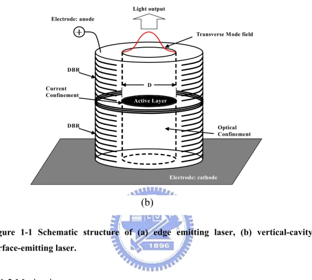
Since the later 1990s, the explosive growth of using email and the World Wide Web has driven the widespread deployment of computer networks. The popularity of the Internet has dramatically increased the amount of interchange and the sharing of information of graphical, audio data, video data and so on. This drastic advance has outgrown the communication infrastructure beyond its current bandwidth capacities (i.e. using LEDs as transmitters). Therefore, the use of high-speed vertical –cavity-surface-emitting lasers (VCSEL) as the replacement for LEDs is the key technology to enable the next generation of low-cost, reliable, and high-speed optical interconnection [1]. Vertical cavity surface emitting lasers (VCSELs) was first demonstrated in 1979 by H. Soda, K. lga, F. Koyama and S. Kinoshita [2]. While the cavity design was novel as compared to the established edge-emitting lasers, the initial device performance was poor in terms of the high threshold current density and low output power that it apparently attracted little attention. Continued work by lga and various coworkers, however, showed continuous improvements in performance, eventually leading to the first continuous wave VCSEL operation, at room temperature, reported in 1988 [3]. By that time other important innovations and demonstrations had brought growing attention to the VCSEL. Figure 1-1 shows the comparison sketch of edge-emitting laser and VCSEL.
The VCSEL structure may provide a number of advantages over traditional lasers, as follow:
z Low threshold operation for its small cavity volume z High-speed modulation capability
z Low power consumption z Low cost chip production
z Easy coupling to optical fiber due to circular beam
z The initial probe test can be performed before separating device into discrete chips
z Densely packed and precisely arranged two-dimensional laser arrays z Higher reliability
z Higher integration
The progress of the vertical cavity surface emitting laser in the late 1990s was very fast, and various applications to optoelectronics. In 1992, VCSELs based on GaAs have been extensively studied some of the 0.98, 0.85 and 0.78 um wavelength devices are now commercialized into optical system. VCSELs are currently to be the ideal laser source for fiber optic applications.
Figure 1-1 A modal of vertical cavity surface emitting laser (VCSEL) DBR DBR Optical Confinement Current Confinement Active Layer D
Transverse Mode field Electrode: anode
Electrode: cathode
Light output
(b)
Figure 1-1 Schematic structure of (a) edge emitting laser, (b) vertical-cavity surface-emitting laser.
1.2 Motivation
Vertical-cavity surface-emitting lasers (VCSELs) have attracted much attention in recent years. Singlemode VCSELs are needed for a number of applications, including high-speed laser printing, optical storage and long-wavelength telecommunications. For oxide-confined VCSELs, the current-confined aperture must be less than 3 μm in diameter to ensure stable singlemode operation [4]. However, the large resistance inherited from the small aperture limits the modulation bandwidth and degrades the high-speed performance. The lifetime of the oxide VCSEL also decreases proportionally as the diameter of the oxide aperture shrinks, even when the device is operated at a reduced current [4]. Methods reported to solve the problem include the increase of higher-order mode loss by surfacerelief etching [5] and hybrid oxide-implanted VCSELs [6, 7]. Recently, a two-dimensional photonic crystal (2-D PC)
structure formed on the VCSEL surface has been investigated as a control method of lateral mode. Singlemode output was realized from larger aperture photonic crystal VCSELs (PC-VCSELs).
The organization of this thesis is as following: In chapter 2, we discuss the theory of photonic crystal VCSEL, According to the effective index model, the number of guided mode of an proton-implanted aperture VCSEL is determined by V value. The measurement set up are described in chapter 3. The experimental results and discussions of PC-VCSEL are presented in chapter 4, 5 and 6. Finally, we give a conclusion of the thesis in chapter 7.
Reference
[1] S. F. Yu, “Analysis and design of vertical cavity surface emitting lasers”, Wiley-Interscience, 2003, pp.18
[2] H. Soda, K. lga, C. Kitahara, and Y. Suematsu, “GaInAsP/InP surface emitting injection lasers, “Japanese Journal of Applied Physics, vol.81, pp.2329-2330, 1979. [3] K. lga, F. Koyama, and S. Kinoshita, “Surface-emitting semiconductor lasers, “IEEE
Journal of Quantum Electronics, vol.24, pp.1845-1855, September 1988.
[4] Hawkins, B.M., Hawthorne III, R.A., Guenter, J.K., Tatum, J.A., and Biard, J.R.: ‘Reliability of various size oxide aperture VCSELs’.
Proc. 52nd Electronic Components and Technology Conf., 2002, pp. 540–550 [5] Haglund, A., Gustavsson, J.S., Vukusic, J., Modh, P., and Larsson, A.: ‘Single
fundamental mode output power exceeding 6 mW from VCSELs with a shallow surface relief’, IEEE Photonics Technol. Lett., 2004, 16, (2), pp. 368–370
[6] Hsueh, T.-H., Kuo, H.-C., Lai, F.-I., Laih, L.-H., and Wang, S.C.: ‘High-speed characteristics of large-area single-transverse-mode vertical-cavity surface-emitting lasers’, Electron. Lett., 2003, 39, (21), pp. 1519–1521
[7] Young, E.W., Choquette, K.D., Chuang, S.L., Geib, K.M., Fischer, A.J., and Allerman, A.A.: ‘Single-transverse-mode vertical-cavity lasers under continuous and pulsed operation’, IEEE Photonics Technol. Lett., 2001, 13, (9), pp. 927–929
Chapter II Theory
2.1 Gain-guiding mechanism
In the early development of a laser with a gain-guiding mechanism is based on a simple fabrication technique that is compatible with the existing technologies of facet emitting lasers [1]. A gain-guiding mechanism can be realized by forming a circular metal contact close to the active layer. The injection carrier concentration defines the gain region to confine the transverse mode. Figure 2-1 shows the schematic of a gain-guided VCSEL. The major advantage of this structure is easy to fabricate, but the transverse confinement of optical field and injection current density is weak so that the corresponding threshold current is high. The threshold current can be improved if the current leakage is minimized along the transverse direction. This can be easily achieved by ion implantation into the p-DBR (but should avoid damaging the active layer) to increase the electrical resistively [2]. Figure 2-2 shows the schematic of an ion implanted VCSEL. As is shown, the ion implanted region is defined selectively to control the flow of the injection current into the active layer. Unfortunately, this configuration of ion-implanted region has no control on the diffusion of carrier concentration along the transverse direction of the active layer. It is possible to apply ion implantation into the active layer, but this well increase the optical absorption loss (i.e., due to scattering of ions) of the device. Moreover, at high-power operation, higher-order transverse nodes can be excited because of the influence of thermal lensing and spatial hole burning of carrier concentration, which are the undesired characteristics of gain-guided VCSELs. The other problem is the electrical resistively of the DBRs, which may increase the heat generation inside the laser cavity. Nonetheless, the attraction of this structure is its planar configuration, which guarantees the simplification in fabrication process and packaging so that low production costs can be maintained and the ion implantation can be executed in any semiconductor materials. Therefore, many manufacturers (Honeywell, etc.) manufactured products using ion implantation technology in their early-state development of VCSEL. The ion implantation technique has also been applied to
fabricate long-wavelength VCSELs [3, 4].
Figure 2-1 Schematic diagram of a gain-guiding VCSEL with circular electrode to confine injection carrier concentration into the active layer.
p-DBR
Implanted region
n-DBR
Active region
contact
substrate
Emission aperture
p-DBR
Implanted region
n-DBR
Active region
contact
substrate
Emission aperture
Figure 2-2 Schematic diagram of a gain-guided VCSEL ion implantation regions to confined injection carrier concentration into the active region.
2.2 Hybrid-guiding mechanism
In order to obtain high-power output, the gain area of the device needs to be increased, which increases the number of transverse modes. Furthermore, the wavelength separation and difference in optical losses between these transverse modes decrease. In the limit of very large emission apertures, there are many transverse modes with wavelengths and losses equal to the plane-wave limits. Combining high-power and single-mode operation is therefore very difficult as we discuss in the previous paragraph. The popular design used to obtain single-mode operation VCSEL are antiguiding-structure concept [5]. The main disadvantage of antiguiding structures is the fundamental mode also induces large radiation losses, and then increasing threshold and limiting maximum output power. Young et al proposed another approach using hybrid implant/oxide VCSELs that support single-mode operation [6]. This schematic structure of hybrid-guided approach is shown in Figure 2-3, which relies on modifying the overlap of the optical mode with the gain profile (also referred to as mode-selective gain) to generate high-power single-mode operation. However, the threshold current (Ith) of this VCSEL is rather high, about 5.8 mA. Jean-Francois P.
Seurin et al report this hybrid-confined structure as implant apertured index-guided VCSEL ( I2-VCSEL ) and demonstrated the results in Laser Focus World [7]. The main advantage of the I2-VCSEL is the independent control of the diameter of the etched gallium arsenide (GaAs) pillbox, which defines the index-guiding aperture, and the diameter of the ion implant, which defines the current aperture, by using different sets of masks. The structure is shown in Figure 2-3 (a). Photolithographic processing enables concise control of the diameters. Contrary to an oxide aperture, the implant aperture is invisible to the optical beam. The current aperture can therefore be made smaller than the index-guide aperture to reduce the overlap of the higher-order modes with the gain profile while at the same time keeping a sufficient fundamental mode/gain overlap. The concept of decoupling the high-order mode with gain is shown in Figure 2-3 (b). As the index-guide diameter is increased, the mode diameters will also increase and the overlap with the gain profile will decrease. Because higher-order modes have a relatively larger amount of their power spreading off center than does the
fundamental mode, they suffer more from this loss of overlap. Eventually, the modal threshold gains of higher-order modes will become too high and the fundamental mode will be the only one to laser.
(a) (b)
Figure 2-3 (a) The schematic structure of implant-aperture index-guided VCSEL (hybrid confinement), current confinement and photon confinement can be controlled independently. (b) The schematic of coupling relationship between transverse mode and gain spectrum.
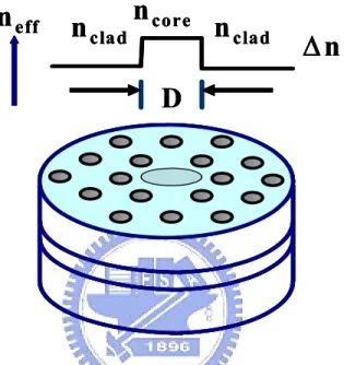
2.3 V-parameter
Lateral-mode control of vertical-cavity surface-emitting lasers (VCSELs) is one of the key issues in realizing high performance optical communication systems, in which single-mode operation is necessary for long and short wavelength regions. High-power single-mode operation is also required for free-space data communication applications. Recently, a two-dimensional photonic crystal (2D PC) structure formed on a VCSEL surface has been investigated as a lateral-mode control method. The most attractive feature of this structure is the enlargement of the emission area, thereby permitting higher power output. The large area can be realized because of strong wavelength dependence of the refractive index in the 2D photonic crystal structure, analogous to the situation in a
photonic crystal fiber. Although good single mode operation has been reported for a specific structure, the optimized design of 2-D photonic crystal structure was not clear, especially when considering a finite etching depth. Since the mode control mechanism utilized in this technology is the effective index control achieved by forming a 2D photonic crystal structure, a parameter representing this control must have a strong dependence, both theoretically and experimentally, of the effective index change in a VCSEL structure.
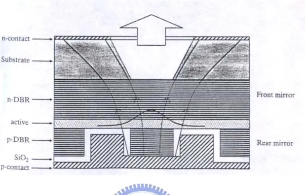
A two-dimensional (2D) photonic crystal structure formed on a VCSEL surface has been investigated as a control method of lateral mode. D. S. Song et al. first applied 2-D photonic crystal on oxide-confined VCSEL, and the schematic structure was shown in Figure 2-4 [3]. This concept was from the endless single-mode from photonic crystal fibers [4]. By introducing the single defect photonic crystal to the VCSEL, a waveguide is expected to be formed around the central defect region where the effective index is larger than the surrounding region. The effective index model [5, 6] is used to understand the VCSEL with lateral structural variation. According to the effective index model, in ref. [3], the number of guided mode of an oxide-confined VCSEL is determined by V parameter, which has the form [6]
2 2 , 2 , 2 2 2 2
(
h
h
)
d
(
k
k
)
d
V
≡
core−
clad≈
〈
ε
〉
clad z−
corez (2-1) where kcore,z , kclad,z , are longitudinal resonance wave vectors of core and cladding region,respectively, and hcore , hclad are transverse wave vector in the medium. d is a diameter of
the core. The〈ε represents the dielectric constant weighted by the longitudinal standing 〉 wave. For the photonic crystal VCSEL shown in Figure 2-3, the resonance wavelengths would be different for central core region and rthe surrounding region. This situation is approximated as a simple step-index waveguide
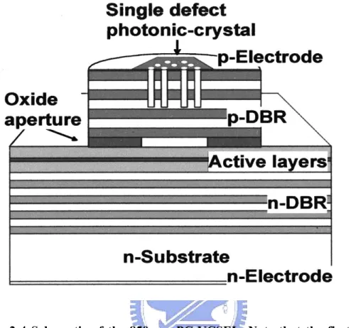
Figure 2-4 Schematic of the 850 nm PC-VCSEL. Note that the first generation PC-VCSEL structure has no oxide current aperture. The oxide aperture is added to the second generation devices for current confinement.
surrounding region. This situation is approximated as a simple step-index waveguide as shown in Figure 2-4. With the aid of this model, the difference of effective indices in the two regions can be estimated by measuring the resonant wavelengths in the core and surrounding regions. The overall effects of the etch diameter, and pitch of the holes show up experimentally as the shift of the resonant wavelength. This may be written compactly as core clad core core eff clad core eff
n
n
, −/
,≈
Δ
λ
−/
λ
Δ
(2-2)PC-VCSEL were Fabricated on selective oxide VCSEL, single-mode output with higher output power were realized from larger aperture [1]. However, those photonic crystal PC-VCSELs exhibit relatively high threshold current (Ith) due to large oxide
confined apertures.
The 2D photonic crystal structure with finite etching depth incorporating a single
point or a seven-point defect is formed in the DBR. It is know that the normalized frequency or V-parameter is useful in evaluating the number of guided modes in cylindrical wave guides, an important example being step index optical fibers. The cutoff condition of the first higher mode leads to V
n
effn
coren
cladn
cladΔn
D
n
effn
effn
coren
cladn
cladn
coren
cladn
cladΔn
D
Figure 2-5 The Schematic of lateral effective index variation provided by the photonic crystal.
eff = 2.405, and thus a wave guide
with Veff < 2.405 is considered to be single mode. In a photonic crystal VCSEL, the
effective V-parameter can be expressed by
(2-3) 2 2
)
(
2
n
n
n
V
eff=
π
Λ
eff−
eff−
γ
Δ
λ
where λ is an operating wavelength, γ is an equivalent defect radius, neff is the
effective index of the VCSEL cavity [9] without a photonic crystal structure present, Dn
the hole depth dependence factor that accounts for finite etching depth of the photonic crystal holes in actual photonic crystal VCSELs. The r factor can be understood qualitatively as proportional to the spatial overlap between the photonic crystal structure. Thus, γ=0 for vanishing etching depth, γ=1 for infinite etching depth, and γ=0.5 for holes reaching the middle of the cavity. In the following discussion, the equivalent defect radii of a single point defect and seven-point defect structures are assumed to be Λ-d/2 and √3Λ-d/2, respectively, where L is lattice constant and d is the hole diameter of a circular hole of the 2-D photonic crystal structure. Since we need to investigate larger d/L ratios than those of PCFs [10], Veff is slightly modified from its
appearance in Ref. 10, with the introduction of the Veff-parameter and the modified r in
Eq. (2-3). The refractive index variation Dn can be obtained from the photonic band
diagram of an out-of-plane propagation mode[11,12], it calculated by assuming that the photonic crystal structure is infinite both in lateral and vertical directions.
Reference
[1] S. F. Yu, “Analysis and design of vertical cavity surface emitting lasers”, Wiley-Interscience, pp.22, 2003.
[2] Y. J. Yang, T. C. Dziura, T. Bradin, S. C. Wang and R. Fernandez, “Continuouswave single transverse mode vertical cavity surface emitting lasers fabricated by Helium implantation and zinc diffusion,” IEE Electron. Lett., vol. 28, no. 3, pp. 274-275, 1992.
[3] J. Boucart, C.Starck, F. Gaborit, A. Plais, N. Bouche, E. Derouin, L. Goldstein, C. Fortin, D. Carpentier, P. Salet, F. Brillouet and J. Jacquet, “1mW CW-RT monolithic VCSEL at 1.55μm,” IEEE Photon. Technol. Lett., Vol. 11, pp.629-631, no.6, 1999.
[4] Y. Qian, Z. H. Zhu, Y. H. Lo, D. L. Huffaker, D. G. Deppe, H. Q. Hou, B. E. Hammons, W. Lin and Y. K. Tu, “Low-threshold proton implanted 1.3μm vertical cavity top surface emitting lasers with dielectric and wafer bonded GaAs-AlAs bragg mirrors,” IEEE Photon. Technol. Lett., vol. 9, no.7, pp.866-868, 1997.
[5] J. W. Scott, B. J. Thibeault, D. B. Young, L. A. Coldren and F. H. Peters, “High efficiency submilliamp vertical cavity lasers with intracavity contacts,” IEEE
Photon. Technol. Lett., vol. 6, no. 6, pp.678-680, 1994.
[6] E. W. Young, K. D. Choquette, S. L. Chuang, K. M. Geib, A. J. Fischer and A. A. Allerman, “Single-transverse-mode vertical-cavity lasers under continuous and pulsed operation,” IEEE Photon. Technol. Lett., vol. 13 pp. 927–929, 2001
[7] J.-F. P. Seurin, S. L. Chuang, L. M. F. Chirovsky, and K. D. Choquette, “NovelVCSEL designs deliver high single-mode output power,” Laser
Focus World, vol. 38, issue 5, 2002.
[8] T. Honda, T. Shirasawa, N. Mochida, A. lnoue, A. Mastsutani, T. Sakaguchi, F. Koyama, and K. lga, “Design and fabrication processes consideration of GaN-based surface emitting lasers“, Trans. IEICE, J81-C-II, pp.97-104,1998.
[9] G..P.Agrawal, Fiber-Optic Communication System~Wiley, New York, 1997.
[10] R.Brand, “10 gigabit Ethernet interconnection with wide area networks,” 10GEA, March 2003.
[11] A.A. Maradudin and A.R. McGurn, J. Mod. Opt. 41, 275~1994.
[12] J.D. Joannopoulos, R.D. Meade, and J.N. Winn, Photonic Crystal-Molding the Flow of Light~Princeton University Press, Princeton, NJ, 1995.
Chapter III Measurement setup
3.1 Probe station and spectrum measurement system
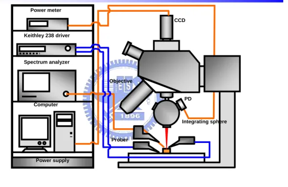
Probe station system was essential instrument for basic characteristics measurement such as I-L (current versus light output), I-V (current versus voltage). We are scheming out the probe station system, illustrated in Figure 3-1, contained probe station, current source, and power-meter module. Keithley 238 as current source supplies continuous current for diode laser and receives relative voltage synchronously. Laser output power is measured by Newport power-meter module (model 1835C). With these data, we could plot the trend of L-I-V curves associated with computer. The light output was detected by a calibrated an integrating sphere with Si photodiode. For accuracy power measurement, an integration sphere was used to pick up whole light output from PC-VCSEL.
For basic measurement, PC- VCSEL device was placed on platform of probe station and injected bias current with microprobe. We could observe threshold condition, slope efficiency, turn-on voltage and differential resistance as L-I-V curves information by sweeping bias current injection. Distribution of transverse mode power is metered as near-field pattern. Near-field pattern (NFP) is still obtained by specific CCD and traces out results with computer. Beam-view analyzer software used in taking NFP. We could obtain NFP image under threshold current, as spontaneous emission, to define oxide aperture size.
Emission spectrum was measured by Advantest optical spectrum analyzer (OSA). We served a multi-mode fiber bundle on probe close to emission aperture in focus for taking spectra. OSA had small spectrum resolution as 0.1nm for accurately measuring PC-VCSEL lasing spectrum. The spectrum measurement system was combined with probe station as showed in Figure 3-1.
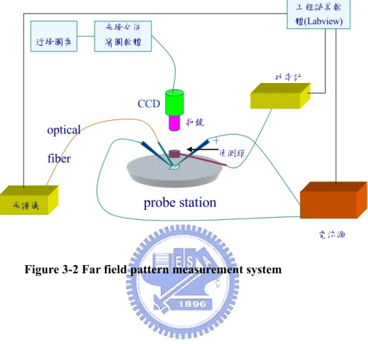
Distribution of divergence angle is metered as far-field pattern. We used a long work distance objective (20X,Nikon), fixed in a triple-divide translation stage, to pick up the laser output from VCSEL. Light was received by CCD (coherent 4800). Far-field pattern (FFP) is still obtained by specific CCD and traces out results with computer. Beam-view analyzer software used in taking FFP. We could obtain FFP image under threshold, to define divergence angle illustrated with Figure 3-2
Power meter
Figure 3-1 Probe station measurement instrument setup
CCD Objective Keithley 238 driver Power supply Spectrum analyzer Computer Integrating sphere PD Prober
+ – 電流源 物鏡 CCD 光譜儀 功率計 近場圖案 工程試算軟 體(Labview) optical fiber 光場分佈 繪圖軟體
probe station
偵測頭Chapter IV Characteristics of singlemode proton-implanted photonic
crystal VCSEL
4.1 Introduction
Vertical-cavity surface-emitting lasers (VCSELs) have attracted much attention in recent years. High-power, singlemode operation is desired for a number of applications, including high-speed laser printing, optical storage and long-wavelength telecommunications. Recently, a two-dimensional photonic crystal (2-D PC) structure formed on a VCSEL surface has been investigated as a lateral-mode control method. The most attractive feature of this structure is the enlargement of the emission area, thereby permitting higher power output. It is critical that PC VCSELs obtain single transverse-mode operation and a small far-field angle for efficient coupling into singlemode fiber. In this study, we designed a low threshold current (Ith), high-power,
single-lateral-mode, low divergent angle operation VCSEL by employing proton implantation combined with a single-point defect photonic crystal index guiding layer. The large area can be realized because of the specifically tailored refractive index induced by the 2D PC structure, analogous to the situation in a PC fiber (PCF). [1] To understand the VCSEL with lateral structure variation, the effective index model is used. According to the effective index model, the number of guided mode of a proton-implanted aperture VCSEL is determined by V parameter which it has the form:
where neq is the equivalent refractive index of the photonic crystal region surrounding the
central defect (determined from band diagram analysis and etching depth dependence), nm is the unmodified index of the defect region, Λ is the lattice constant, λ is the free-space wavelength [2][3]. If Veff is less than 2.405, the structure is considered to be
singlemode. In general, an increase in diameter of hole with a given lattice constant or an increase in the size of the central defect will increase the likelihood of laser operation in multiple higher order transverse modes, rather than the lowest order single transverse mode operating point.
4.2 Device fabrication
The epitaxial layers of the PC-VCSELs wafer structure were grown on the
n+-GaAs substrate by a metal organic chemical vapor deposition (MOCVD) system. The bottom distributed Bragg reflector (DBR) consists of a 30.5-pair n-type (Si-doped) quarter-wave stack of Al0.12Ga0.88As/AlAs. The top DBR consists of 22-period p-doped
(carbon-doped) Al0.12Ga0.88As/AlA quarter-wave stack. Above that, a heavily-doped
p-type GaAs contact layer. The graded-index separate-confinement heterostructure (GRINSCH) GaAs/AlGaAs active region has an undoped three-quantum-well (3 QWs) GaAs/Al0.3Ga0.7As, a lower linearly-graded undoped Al Gax 1-xAs (x = 0.6Æ0.3)
waveguide layer and an upper linearly-graded undoped-Al Gax 1-xAs (x=0.3Æ0.6)
waveguide layer. The proton (H+)-implanted VCSEL was fabricated before
combination with photonic crystal holes. Firstly was then, the p-contact ring with an inner diameter of 24 to 46 µm was deposited on the top of p-contact layer and n-contact was deposited on the bottom of n+-GaAs substrate. The device was annealed in thermal annealing system at 430 under N℃ 2 ambient for 30 sec. The current
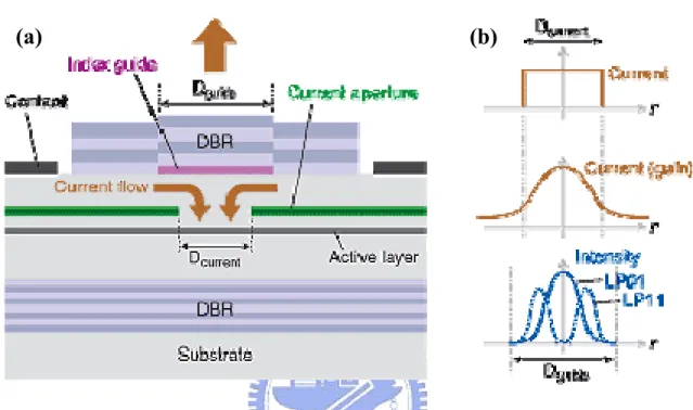
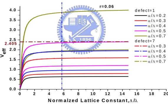
confinement of the device, with a diameter of 10 μm, was then defined by proton implantation. The implantation energy was 270 keV, with a dosage of 6×1014 cm-2. After that, hexagonal lattice patterns of photonic crystal with a single- or seven-point defect were defined within the p-contact ring using photo-lithography and etched through the p-type DBR by using reactive ion etch (RIE). The lateral index around a single defect can be controlled by the hole diameter (α) -to-lattice constant (Λ) ratio and etching depth [4]. The ratios for fabricating are referred to ref. [4] and [5].
The relation of the normalize lattice constant and Veff were calculated by using the
from 0.2 to 0.7 and the defects are 1 and 7 point defects. γ is an etching depth dependence factor. By using the γ-factor, the effective index ( ) of the PC-VCSEL structure can be written as
clad eff n , core eff core eff clad eff n n n , = , −γΔ , . γ varies from 0 to
1 depending on the etching depth and structure. In our structure, the etching depth of the holes is about 17 pairs and the γ is 0.06. As shown in Figure 4-1, when the ratios (α/Λ) change from 0.2 to 0.7 with one point defect, the Veff parameter all under
single-mode guiding condition of 2.405. For 7 point defects, the ratios (α/Λ) below 0.5 are all suitable single-mode guiding condition, but when the ratio (α/Λ) is larger than 0.5, the guiding condition is
0 2 4 6 8 1 0 1 2 1 4 1 6 1 8 2 0 0 .0 0 .5 1 .0 1 .5 2 .0 2 .5 3 .0 3 .5 4 .0 r= 0 .0 6
Figure 4-1 Veff parameters for r=0.06, which correspond to etching depths of 17 pairs, are calculated.
multi-mode. Therefore, we designed the lattice constant Λ is 5 μm in the PC-VCSEL and the etching depth of the holes is about 17 pairs of the top DBR. The device structure is shown in Figure 4-2. By using two types of apertures in this device, we decouple the
2 .4 0 5 d e f e c t= 1 α/Λ= 0 .2 α/Λ= 0 .3 α/Λ= 0 .4 α/Λ= 0 .5 α/Λ= 0 .7 d e f e c t= 7 α/Λ= 0 .3 α/Λ= 0 .4 α/Λ= 0 .5 α/Λ= 0 .7 V ef f N o r m a lz e d L a ttic e C o n s ta n t,Λ/λ
effects of the current confinement from the optical confinement. The H+ implant aperture of 10 µm is used to confine the current flow, while the single- or seven-point defect (≥ 10 µm in diameter) photonic crystal is used to confine the optical mode. The mechanism of In order to clarify the effect of photonic crystal index-guiding layer, a VCSEL with H+ implant aperture (10 µm in diameter without photonic crystal) was also fabricated for comparison.
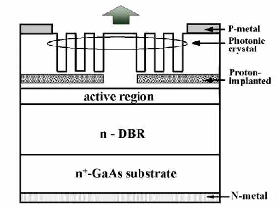
Figure 4-2 Schematic of PC-VCSEL. The hole depth of PC is 17 pairs out of 22 pairs of top DBR been etched off. The proton implantation position is 3 pairs of DBR layers above action region
4.3 Results and Discussions
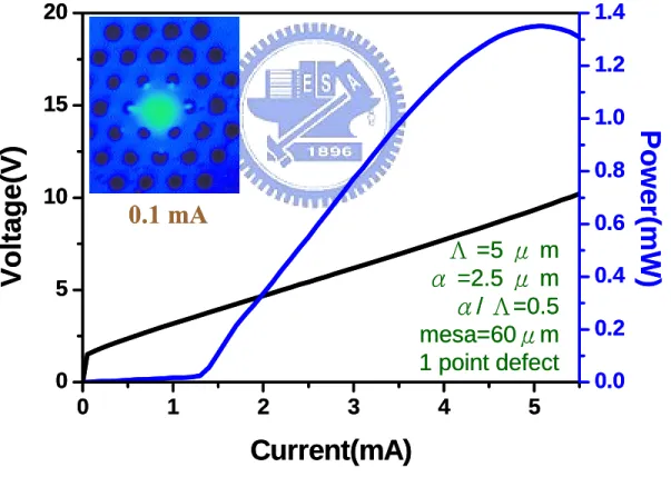
Figure 4-3 shows CW light-current-voltage (L-I-V) output and near-field image operated at 0.1 mA (inset) of the PC-VCSEL. The VCSEL emits over 1 mW peak power and exhibits single modes throughout the current range of operation. The threshold current (Ith) of the PC-VCSEL is 1.25 mA and the slop efficiency is
approximately 0.18 W/A. The I-V characteristic exhibits higher series resistance of the PC-VCSEL which should be mainly due to proton implantation through the p-ohmic contact of the device and the region of current flow were damaged by photonic crystal holes. The output power could be improved by reducing the series resistance of the PC-VCSEL. 0 1 2 3 4 5 0 5 10 15 20
Current(mA)
Voltage
(V)
0.0 0.2 0.4 0.6 0.8 1.0 1.2 1.4Po
wer(
mW)
Λ =5 μ m
α =2.5 μ m
α/ Λ=0.5
mesa=60μm
1 point defect
0.1 mA
0 1 2 3 4 5 0 5 10 15 20Current(mA)
Voltage
(V)
0.0 0.2 0.4 0.6 0.8 1.0 1.2 1.4Po
wer(
mW)
Λ =5 μ m
α =2.5 μ m
α/ Λ=0.5
mesa=60μm
1 point defect
0.1 mA
Figure 4-3 CW L-I-V characteristics and near-field image (inset) of a PC-VCSEL. The ratio (α/Λ) is 0.5 and the lattice constant Λ is 5 μm
.
836 838 840 842 844 -70 -60 -50 -40 -30 -20 -10 0 1.5mA 2.5mA 4mA 5mA
Inte
nsity(
dB
)
Wavelength(nm)
(a)
(b)
Figure 4-4 Spectra of the proton-implanted (a) photonic crystal VCSEL with ratio (α/Λ) is 0.5 and the lattice constant Λ is 5 μm and (b) VCSEL without
Lasing spectra of the PC-VCSEL is shown in Figure 4-4 (a), confirming single-mode operation within overall operation current. The PC-VCSEL reveals side mode suppression ratio (SMSR) > 40dB throughout the current range. For comparison, a lasing spectra of proton implanted VCSEL without photonic crystal holes shows multiple mode operation as the driving current increased above 4.25 mA (Figure 4-4 (b)). As the driving current increases, even higher order transverse mode emerges. The pulsed L-I characteristics of the PC-VCSEL is also measured and the maximum output power is exceeding 2 mW (not shown here). Temperature-dependent measurements are underway to verify the non-linearity characteristics. Figure 4-5 shows the lasing spectrum of seven-point defects condition and exhibits the single-mode output.
830 832 834 836 838 840 842 844 846 848 20 30 40 50 60 70 80 90 0 2 4 6 8 10 0 2 4 6 8 10 12 0.0 0.1 0.2 0.3 0.4 0.5 0.6 0.7 Current (mA) Vol tage ( V ) Po w e r ( m W ) mesa=68μm Λ=5μm, α=2.5μm 7 point defect
In
te
ni
st
y (
a
.u
)
1.5mA 2 mA 4 mA 6 mA 8 mAWavelength (nm)
Figure 4-5 Spectra of the proton-implanted VCSEL with photonic crystal of seven-point defects. The ratio (α/Λ) is 0.5, and the lattice constant Λ is 5 μm. The
The divergence angles of far-field pattern of proton-implanted VCSEL with and without photonic crystal on it are measured for comparison and shown in Figure 4-6. As shown in Figure 4-6 (a), the divergent angles of the proton-implanted multi-mode VCSEL were increase with the increasing operation current and the divergent angles are over 17o. But for proton-implanted VCSEL with photonic crystal as shown in
Figure 4-6 (b), the divergence angles are around 6.5o, and are persistent even when the
applied current is increased. The divergent angle is smaller than the conventional oxide-confined single-mode VCSEL and exhibit superior guiding effect of photonic crystal 0 30 60 90 120 150 180 0 30 60 90 120 150 180 0 30 60 90 120 150 180 (a) without photonic crystal (b) with photonic crystal
I=4mA I=6mA I=7mA
16.9 ° 19.2 ° 20.6° 6.46° 6.48 ° 6.50° 0 30 60 90 120 150 180 0 30 60 90 120 150 180 0 30 60 90 120 150 180
Figure 4-6 Divergent angles of the proton-implanted VCSEL (a) without and (b) with photonic crystal.
4.4 Conclusion
We report a high power (>1mW) single mode PC-VCSEL with SMSR >40dB throughout the operation current range and used the effective index model to estimate the index difference between the core cladding ranges. This PC-VCSEL, with an aperture of about 10 um, has ultra-low threshold current of about 1.25 mA. The FWHM far-field angle is 6.5° at I=5 mA. The present results indicate that a VCSEL using proton
implantation for current confinement and photonic crystal for optical confinement is a reliable approach to achieve high-power singlemode operation of a VCSEL.
References
[1] T.A. Birks, J.C. Knight, and P. St. J. Russell, Opt. Lett.82, 1344 (2003)
[2] N.Yokouchi, A.J. Danner, and K.D. Choqueete, Appl. Phys. Lett. 22, 961 (2003) [3] T.A. Birks, J.C. Knight, and P. St. J. Russell, Opt. Lett.22, 961 (1997)
[4] N. Yokouchi, , A. J. Danner and K. D. Choquette, “Etching depth dependence of the effective refractive index in two-dimensional photonic-crystal-patterned vertical-cavity surface-emitting laser structures,” Appl. Phys. Lett., vol. 82, pp. 1344-1346, 2003
[5] D. Berkedal, N. Gregersen, S. Bischoff, M. Madsen, F. Romsted, J. Oestergarrd, “Large-area single-mode photonic bandgap VCSELs,” Proc. Optical Fiber Communications Conf., Atlanta, GA, USA, 2003, pp. 83–85, 2003
Chapter V Characteristics of singlemode InGaAs Sub-Monolayer
quantum dot photonic crystal VCSEL
5.1 Introduction
Vertical-cavity surface-emitting lasers (VCSELs) have attracted a lot of attention in recent years. Single-mode VCSELs are necessary for a number of applications, including high-speed laser printing, optical storage and long-wavelength telecommunications. Small oxide aperture VCSELs below about 4 μm diameter operate in the fundamental transverse mode. However, the large resistance inherited from the small aperture limits the modulation bandwidth and degrades the high-speed performance. The lifetime of the oxide VCSEL also decreases proportionally to the diameter of the oxide aperture, even when the device is operated at a reduced current.[1] When the aperture diameter is increased to obtain higher output power, however, multiple higher-order transverse modes oscillate, causing increased noise, a broadened spectrum, and a strong increase of the far-field angle. Techniques used to solve the problem include the increase of higher order mode loss by surface-relief etching [2], hybrid oxide-implanted VCSELs [3,4] and two-dimensional triangular holey structure.[5] Recently, two-dimensional photonic crystal (2D PC) structure formed on the VCSEL surface has been used as a control method of transverse modes. Single-mode output was realized from larger aperture photonic crystal VCSELs (PC-VCSELs) [6,7]. However, those PC-VCSELs exhibit relatively high threshold currents (Ith) due to large oxide confined apertures. For long-wavelength applications,
InAs quantum-dot (QD) VCSELs[8] and QD PhC-VCSELs[9] achieved laser emission at 1300 nm. For shorter wavelength emission, InGaAs/GaAs sub-monolayer (SML) quantum dot (QD), embedded in a GaAs matrix shows luminescence peaks and high power lasing performance in the 0.92 – 1 μm range [10].
Recently single-mode InGaAs SML QD VCSELs with room-temperature output power as high as 4 mW have been demonstrated [11]. However singlemode operation of the InGaAs SML QD VCSEL with PC is still yet to be realized. In this paper, we report our results on the InGaAs QD PC-VCSELs in the 990 nm range. Single-transverse-mode operation with very high side-mode suppression ratio (SMSR) is demonstrated for the first time. The beam profile characteristics of the devices were also measured and analyzed.
5.2 Device fabrication
The epitaxial layers of the InGaAs SML QD PhC-VCSEL wafers were grown on 3 inch n+-GaAs (001) substrates by molecular beam epitaxy (MBE) in Riber 49 chamber. The bottom distributed Bragg reflector (DBR) consists of a 33-pair n-type (Si-doped) quarter-wave stack (λ/4) of Al0.9Ga0.1As/GaAs. The top DBR consists of
20-period p-type (carbon-doped) Al0.9Ga0.1As/GaAs quarter-wave stack. Above that is
a heavily doped p-type GaAs contact layer. The undoped 1λ-cavity contains 3 InGaAs SML QD layers, separated by GaAs barrier layers. Each of the InGaAs SML QD layer is formed by alternate deposition of InAs (<1 ML) and GaAs. The current confinement of the device was done by the selectively oxidized AlOx tapered-aperture.
Firstly, mesas with diameters varied from 50 to 68 μm was defined by reactive ion etch (RIE). The p-contact ring with an inner diameter 4 μm larger than the oxide aperture was formed on the top of p-contact layer. The AlAs layer within the Al0.9Ga0.1As confinement layers was selectively oxidized to AlOx. The oxidation
depth was about 15 μm toward the center from the mesa edge so that the resulting oxide aperture varied from 20 to 38 μm in diameter. The oxide aperture was introduced in minimum of optical field in order to reduce the lateral optical loss and the leakage current. The n-contact was formed at the bottom of the n+-GaAs substrate.
After that, triangular lattice patterns of photonic crystal with a single-point defect in the center were defined within the p-contact ring using photo-lithography and etched through the p-type DBR using RIE. The lateral index around a single defect can be
controlled by the hole diameter (α) -to-lattice constant (Λ) ratio and etching depth [6]. This ratio (α/Λ) is 0.5; the lattice constant Λ is 5 μm in the PC-VCSEL and the etching depth of the holes is about 16-pair thick into the 20-pair top DBR layer. The device structure is shown in Fig. 5-2. By using two types of apertures in this device, we decouple the effects of the current confinement from the optical confinement. The AlOx layer is used to confine the current flow, while the single-point defect
(approximately ≥ 10 µm in diameter) photonic crystal is used to confine the optical mode. In order to clarify the effect of photonic crystal index-guiding layer, an oxide-confined VCSEL (oxide aperture = 20 µm in diameter without PC) was also fabricated for comparison. The relation of the normalize lattice constant and Veff were
calculated by using the Rsoft-BandSOLVE software and shown in Figure 5-1. The ratios (α/Λ) are changed from 0.2 to 0.7 and the defects are 1 and 7 point defects. γ is an etching depth dependence factor. By using the γ-factor, the effective index ( ) of the VCSEL structure can be written as
clad eff n , core eff core eff clad eff n n n , = , −γΔ , . γ varies from 0
to 1 depending on the etching depth and structure. In our structure, the etching depth of the holes is about 17 pairs and the γ is 0.06. As shown in Figure 5-1, when the ratios (α/Λ) change from 0.2 to 0.7 with one point defect, the Veff parameter all under
single-mode guiding condition of 2.405.
0 2 4 6 8 10 0.0 0.5 1.0 1.5 2.0 2.5 3.0 r=0.06 2.406 a/Λ=0.2 defect=1 a/Λ=0.3 defect=1 a/Λ=0.4 defect=1 a/Λ=0.5 defect=1 a/Λ=0.7 defect=1 V ef f
Normalzed Lattice Constant,Λ/λ
Figure 5-1 Veff parameters forγ=0.06, which correspond to etching depths of 17 pairs, are calculated.
Figure 5-2 Schematic of PC-VCSEL. The hole depth of PC is 16 pairs out of 20 pairs of top DBR been etched off.
5.3 Results and Discussions
Fig. 5-3 shows continuous-wave (CW) light-current-voltage (L-I-V) output of the InGaAs SML QD VCSEL without photonic crystal (PC). The mesa of the VCSEL is 50 μm in diameter. The VCSEL shows a peak power of 12.2 mW at 30 mA, with a threshold current (Ith) of 1 mA. The differential series resistance is approximately 100
Ω at 12 mA.
Fig. 5-4 shows CW L-I-V output of the PC-VCSEL. The near-field image of the PC-VCSEL operated at 4 mA is also shown (inset). The mesa of the VCSEL is also 50 μm. The PC-VCSEL emits 3.8 mW maximum power at 28 mA and exhibits single modes operation throughout the current range of operation. The near-field image of the lasing output remains to be fundamental TEM00 mode at the center of the PC
emission from photonic crystal holes surrounding the single-defect area was also observed. This strayed laser emission from the photonic crystal holes corresponds to off-axis laser beam deviated from the optical axis perpendicular to the top-emitting surface of the VCSEL.12) The optical axis is defined to be the main axis of resonance cavity of the VCSEL, which is perpendicular to the top-emitting surface. The Ith of the
PC-VCSEL is 0.9 mA. The differential series resistance of the PC-VCSEL is approximately 125 Ω at 12 mA. The I-V characteristics exhibit slightly higher series resistance for the PC-VCSEL, which should be mainly due to blocking of the current flow in the region by photonic crystal holes.
Lasing spectra of the PC-VCSEL is shown in Fig. 5-5, confirming single-mode operation within overall operation current. The peak lasing wavelengths are 991, 992, and 996 nm at 3 mA, 9 mA, and 20 mA, respectively. The PC-VCSEL exhibits a SMSR > 35dB throughout the current range.
For comparison, lasing spectra of the InGaAs SML QD VCSEL without photonic crystal holes shows multiple mode operation as the driving current is increased above Ith (Fig. 5-6). The InGaAs SML QD VCSEL without PC shows
multiple transverse mode characteristics with a broader wavelength span. Fig. 5-7(a) is the photograph of the near-field image at 10 mA, with light illumination in order to show the laser emission pattern and the photonic crystal structure simultaneously. The near-field image at 14mA is shown in Fig. 5-7(b), and its three-dimensional near-field pattern shown in Fig. 5-7(c). The ratio α/Λ of photonic crystal is 0.5 and the lattice constant Λ is 5 μm. The laser beam emits not only from the single-point defect area at the center of the photonic crystal structure, but also from the six nearby photonic crystal holes. The three-dimensional near-field profile in Fig. 5-7(c) shows the laser output consists of one TEM00 mode emission at the center and six smaller beams with
before thermal rollover occurs. The strayed laser emission from the photonic crystal holes is originated from the off-axis laser resonance within the laser cavity. Most of the laser resonance within the laser cavity of the device is parallel to the optical axis perpendicular to the top-emitting surface[12]. The laser resonance that is not parallel to the optical axis is referred to as the off-axis resonance. The reflectivity of the remaining p-DBR layers under the photonic crystal hole region is significantly reduced due to RIE etch. The resonance under the photonic crystal hole region cannot achieve laser emission because of the insufficient gain within that portion of the cavity. Therefore the laser emission from the photonic crystal holes must be contributed from off-axis laser resonance and diffraction within the laser cavity. The measured spectra in Fig. 5-5 indicate that all the laser emission beams, including those from the photonic crystal holes, are of the same peak lasing wavelength. The spectral single-mode characteristics of the PC-VCSEL are not affected by the laser emission from the photonic crystal holes.
The beam profile results obtained from the far-field beam pattern measurements are shown in Figs. 5-8~5-10. The beam profiles of the PC-VCSEL are shown in Fig. 5-8. The beam divergence angle obtained from the beam profile of the device remains to be 6.7 to 6.9°. The beam intensity increases with increasing current. This very small divergence angle indicates that the laser beam is well confined by the photonic structure of the device. Fig. 5-9 shows the beam profiles of the VCSEL without PC at 3 mA, 7 mA, and 10 mA. The beam intensity increases with increasing current. The beam divergence angle increases from 17.2° at 3 mA to 21.5° at 10 mA. The two laser emission lobes correspond to the multi-mode laser emission, as observed by the multi-mode spectra in Fig. 5-6. Fig. 5-10 shows the current-dependent divergence angle of the InGaAs SML QD PC-VCSEL and InGaAs SML QD VCSEL without PC. For the InGaAs SML QD PC-VCSEL, the beam
divergence angle remains to be very small and almost unchanged within 6.7° to 6.9°, with respect to current increase. For the InGaAs SML QD VCSEL without PC, the divergence angle increases monotonically with increasing current.
Figure 5-3 CW L-I-V characteristics without Photonic Crystal
Figure 5-4 CW L-I-V characteristics and near-field image of PC-VCSEL at 4 mA. The ratio (α/Λ) is 0.5 and the lattice constant Λ is 5 um.
Figure 5-5 Spectra of PC VCSEL
(a)
(b)
(c)
Figure 5-7 Near Field image and the ratio (α/Λ) is 0.5 and the lattice constant Λ
Figure 5-8 Normalized intensity against far-field angle at various current with Photonic Crystal
Figure 5-9 Normalized intensity against far-field angle at various current without Photonic Crystal
Figure 5-10 Far-field angle against CW current at various with PC and without PC
5.4 Conclusion
We report a single-mode InGaAs SML QD PC-VCSEL with SMSR > 35 dB throughout the operation current range. A maximum single-mode output power of 3.8 mW has been demonstrated. The present results indicate that a VCSEL using an oxide layer for current confinement and photonic crystal for optical confinement is a promising approach to achieve single-mode operation of VCSEL. The beam profile and near-field image study of the PC-VCSEL indicates that the laser beam is well confined by the photonic crystal structure of the device.
Reference
52nd Electron. Comps. & Technol. Conf., Proc. (2002) p.540.
[2] A. Haglund, J. S. Gustavsson, J. Vukusic´, P. Modh and A. Larsson: IEEE Photon. Technol. Lett. 16 (2004) 368.
[3] T. H. Hsueh, H. C. Kuo, F. I. Lai, L. H. Laih and S. C. Wang: Electron. Lett. 39 (2003) 1519.
[4] E. W. Young, K. D. Choquette, S. L. Chuang, K. M. Geib, A. J. Fischer and A. A. Allerman: IEEE Photon. Technol. Lett. 13 (2001) 927.
[5] A. Furukawa,S.Sasaki,M.Hoshi,A.Matsuzono,K.MoritohandT.Baba: Appl. Phys. Lett. 85 (2004) 5161.
[6] N. Yokouchi, A. J. Danner and K. D. Choquette: Appl. Phys. Lett. 82 (2003) 1344.
[7] D. Berkedal, N. Gregersen, S. Bischoff, M. Madsen, F. Romsted and J. Oestergarrd: Optical Fiber Comm. Conf. Proc. (2003) p.83.
[8] J. A. Lott, N. N. Ledentsov, V. M. Ustinov, N. A. Maleev, A. E. Zhukov, A. R. Kovsh, M. V. Maximov, B. V. Volvovik, Z. H. I. Alferov and D. Bimberg: Electron. Lett. 36 (2000) 1384.
[9] H. P. D. Yang, Y. H. Chang, F. I. Lai, H. C. Yu, Y. J. Hsu, G. Lin, R. S. Hsiao, H. C. Kuo, S. C. Wang and J. Y. Chi: Electron. Lett. 41 (2005) 1130.
[10] S. S. Mikhrin, A. E. Zhukov, A. R. Kovsh, N. A. Maleev, V. M. Ustinov, Yu. M. Shernyakov, I. P. Soshnikov, D. A. Livshits, I. S. Tarasov, D. A. Bedarev, B. V. Volovik, M. V. Maximov, A. F. Tsatsul’nikov, N. N. Ledentsov, P. S. Kop’ev, D. Bimberg and Z. H. I. Alferov: Semicond. Sci. Technol. 15 (2000) 1061.
[11] S. A. Blokhin , N. A. Maleev, A. G. Kuzmenkov, Yu. M. Shernyakov, I. I. Novikov, N. Yu. Gordeev, G. S. Sokolovskii, V. V. Dudelev, V. I. Kuchinskii, M. M. Kulagina, M. V. Maximov, V. M. Ustinov, A. R. Kovsh, S. S. Mikhrin and N.
N. Ledentsov: Semiconductors 40 (2006) 663.
Chapter VI Singlemode InAs quantum dot photonic crystal
VCSELs
6.1 Introduction
Vertical-cavity surface-emitting lasers (VCSELs) have attracted much attention in recent years. Singlemode VCSELs are needed for a number of applications, including high-speed laser printing, optical storage and long-wavelength telecommunications. For oxide-confined VCSELs, the current-confined aperture must be less than 3 um in diameter to ensure stable singlemode operation [1]. However, the large resistance inherited from the small aperture limits the modulation bandwidth and degrades the high-speed performance. The lifetime of the oxide VCSEL also decreases proportionally as the diameter of the oxide aperture shrinks, even when the device is operated at a reduced current [1]. Methods reported to solve the problem include the increase of higher-order mode loss by surfacerelief etching [2] and hybrid oxide-implanted VCSELs [3, 4]. Recently, a two-dimensional photonic crystal (2-D PC) structure formed on the VCSEL surface has been investigated as a control method of lateral mode. Singlemode output was realised from larger aperture photonic crystal VCSELs (PC-VCSELs) [5, 6]. However, those PC-VCSELs exhibit relatively high threshold currents (Ith) owing to large oxide-confined apertures. For
long-wavelength applications, InGaNAs [7, 8] and InAs-InGaAs quantum dot (QD) VCSELs [9] achieved laser emission at 1300 nm. Singlemode operation of the QD VCSEL with PC is yet to be realized. In this Letter, we report our results on the QD PC-VCSELs in the 1300 nm range. Single-lateral-mode operation with very high side-mode suppression ratio (SMSR) is demonstrated for the first time.
6.2 Device fabrication
The epitaxial layers of the QD PC-VCSEL wafers were grown on n+-GaAs substrates by molecular beam epitaxy (MBE). The bottom distributed Bragg reflector (DBR) consists of a 33.5-pair n-type (Si-doped) quarter-wave stack ( λ /4) of Al0.9Ga0.1As/GaAs. The top DBR consists of a 23-period p-type (carbon-doped)
Al0.9Ga0.1As /GaAs quarter-wave stack. Above that, is a heavily doped p-type GaAs
contact layer. The active region contains 17 undoped InAs-InGaAs QD layers, separated by GaAs barrier layers. Each of the InAs-InGaAs QD layers consists of 2.5 monolayer-thick InAs pyramidal islands and a 5 nm-thick In0.15Ga0.85As quantum well
overgrowth layer. The current confinement of the device was achieved by combining selective oxidation with proton (H+)-implantation. First, mesas with diameters varied from 44 to 68 um were defined by reactive ion etch (RIE). The AlAs layer within the Al0.9Ga0.1As confinement layers was selectively oxidised to AlOx. The oxidation
depth was about 12 mm towards the centre from the mesa edge so that
the resulting oxide aperture varied from 20 to 44 mm in diameter. The oxide aperture was introduced to reduce the lateral optical loss and the leakage current. The p-contact ring with an inner diameter 2 mm larger than the oxide aperture was formed on the top of the p-contact layer. The n-contact was formed at the bottom of the n+-GaAs substrate. After that, triangular lattice patterns of photonic crystal with a singlepoint defect in the centre were defined within the p-contact ring using photolithography and etched through the p-type DBR using RIE. The lateral index around a single defect can be controlled by the hole diameter (α)-to-lattice constant (Λ) ratio and etching depth [5]. This ratio (α/Λ) is 0.5; the lattice constantΛis 5 um in the PC-VCSEL and the etching depth of the holes is about 18 pairs thick into the 23-pair top DBR layer. To ensure better current confinement of the device, proton implantation was
carried out with a diameter of 12 um, followed by an annealing at 430oC under N2 ambient. The implantation energy was 240 keV, with a dose of 6×1014 cm2, to form an insulating region laying 10 DBR pairs above the active region. Higher implantation energy may introduce more defects in the lateral direction. The device structure is shown in Fig. 6-2. By using two types of apertures in this device, we decouple the effects of the current confinement from the optical confinement. The Ht implant aperture (12 um) and the AlOx layer are used to confine the current flow, while the single-point defect (≧12 um in diameter) photonic crystal is used to confine the optical mode. To clarify the effect of the photonic crystal index-guiding layer, a VCSEL with H+ implant aperture (12 um in diameter without PC) was also fabricated for comparison. The relation of the normalize lattice constant and Veff were calculated
by software of Rsoft-BandSOLVE and shown in Figure 6-1. The ratios (α/Λ) are changed from 0.2 to 0.7 and the defects are 1 and 7 point defects. γ is an etching depth dependence factor. By using the γ-factor, the effective index ( ) of the VCSEL structure can be written as
clad eff n , core eff core eff clad eff n n n , = , −γΔ , . γ varies from 0 to 1
depending on the etching depth and structure. In our structure, the etching depth of the holes is about 17 pairs and the γ is 0.06. As shown in Figure 6-1, when the ratios (α/Λ) change from 0.2 to 0.7 with one point defect, the Veff parameter all under single-mode
0 2 4 6 8 10 0.0 0.5 1.0 1.5 2.0 2.5 3.0 2.406
r=0.06
a/Λ=0.2 defect=1 a/Λ=0.3 defect=1 a/Λ=0.4 defect=1 a/Λ=0.5 defect=1 a/Λ=0.7 defect=1 V ef fNormalzed Lattice Constant,Λ/λ
Figure 6-1 Veff parameters forγ=0.06, which correspond to etching depths of 18 pairs, are calculated.
Figure 6-2 Schematic of QD PC-VCSEL. Hole etching depth of PC is 18 pairs out of the 23-pair top DBR having been etched off. The proton implantation position is 10 pairs of DBR layers above active region.