1
Content
Goals of the 1
stYear Project
Achievements and Discussions
I. Photonic Crystal (PhC) Hetero-Slab-Edge (HSE) Microcavity with High Quality (Q) and Index Sensitivity Surface Mode
(I) PhC HSE Microcavity Laser with High Q Surface Mode
(II) High Index Sensitivity of Surface Mode in PhC HSE Microcavity Laser via Detecting CO2 Gas
II. Square-PhC Point-Shifted D0 Nanocavity for Protein and Nano-Particle Detection
(I) Design and Modal Properties of Square-PhC Point-Shifted D0 Nanocavity Laser (II) Protein Adsorption Detection from Modes in PhC D0 Nanocavity
(III) Spectrum-Free Detection of Nano-Particle by PhC D0 Nanocavity
III. PhC Microcavities for Optically Sensing Stress
(I) Design Principle for Optically Sensing Stress by PhC Microcavity
(II) Modal Properties of Double-Layered PhC Microcavity and its Stress Sensing Application
Achievement Summary
Future Work for the 2
ndYear Project
2
Goals of the 1
stYear Project
This project is focused on the realizations of highly sensitive optical index, bio, andstress sensors by photonic crystal (PhC) micro- and nano-cavities. Owing to the condensed size of PhC cavities, we expect the sensors can be with high sensitivity, small device sizes, and feasible for integrated chip.
In the proposal, for the 1st year, we proposed two brand new blueprints of PhC cavity designs and the goals listed including:
1. Surface mode in PhC slab-edge
(1) (Numerical Simulation) Design of Slab-Edge Microcavity & Modal Properties of Surface Mode
(2) (Experiments) Investigation on Modal Properties (3) (Experiments) Index Sensing Measurement Systems
2. Double-layered PhC microcavity
(1) (Numerical Simulation) Modal Properties of Vertical-Coupled PhC Microcavity Slabs
We have reached all above goals in the 1st year project duration. The detailed description of our achievements is provided in the following sections.
Achievements and Discussions
I. P
HOTONICC
RYSTAL (P
HC
)H
ETERO-S
LAB-E
DGE (HSE
)M
ICROCAVITIESWITH
H
IGHQ
UALITY (Q) ANDI
NDEXS
ENSITIVITYS
URFACEM
ODEVery recently, high-sensitivity Rn and condensed index sensors based on PhC defect micro- and nano-cavities have been demonstrated and optimized theoretically, which show the abilities of sensing very small index variation in very condensed size. However, most of recent reports are based on defect modes confined in cavities (dielectric region), which limit the Rn value. Intuitively, a PhC microcavity with surface wave would be a very good candidate because the mode field extends into environmental material, which has not been addressed and discussed in literatures.
In this section, we propose a PhC hetero-slab-edge (HSE) microcavity design, where the surface mode is confined by mode-gap effect. Optimizations of quality (Q) factor and Rn of surface mode in simulations are achieved. Surface mode lasing actions are also observed. Besides, high Rn value of the surface mode is experimentally confirmed via detecting CO2 gas under different gas pressures.
3
(I) PhC HSE Microcavity Laser with High Q Surface Mode
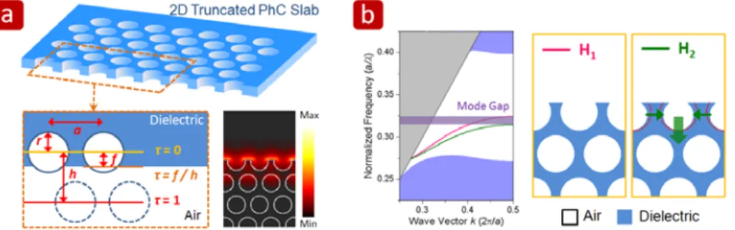
In a two-dimensional (2D) truncated PhC slab shown in Fig. 1a, the surface wave will form and propagate along the interface between the dielectric PhC slab and air due to total-internal reflection and photonic band gap effects, as shown by the simulated electric field distribution in the inset of Fig. 1a. The definition of slab-edge termination parameter τ is also shown. To well confine this surface wave in a slab-edge segment with finite length, two different slab-edges H1 and H2 are used to form the mirror layer by mode gap effect, as shown in Fig. 1b. For a given H1 PhC slab-edge, the H2 slab-edge is obtained by shrinking and shifting the air holes at the slab-edge of H1. In the band diagram of Fig. 1b, the allowed surface mode frequency in H2 will shift to be lower than that in H1. And the mode gap denoted by a shadow region in Fig. 1b will form due to this frequency difference between
H1 and H2. Thus, the surface mode in H1 with frequency inside the mode gap cannot propagate in H2 and H2 can serve as a mirror layer.
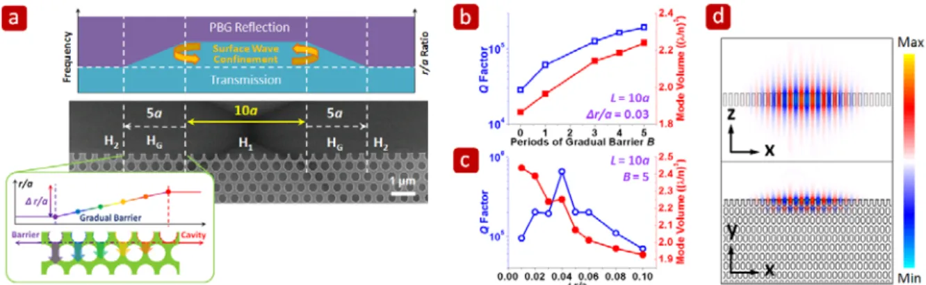
By applying double hetero-interfaces mentioned above, we design a PhC HSE microcavity with high Q factor surface mode, as shown by the scanning electron microscope (SEM) picture in Fig. 2a. The surface mode in microcavity region with slab-edge H1 will be confined by mode gap effect provided by the gradually-varying and outer barriers with slab-edges HG and H2. For HG, the radii and positions of air holes at the slab-edge are shrunk and shifted gradually and linearly, as shown in the inset of Fig. 2a. The air-hole radius (r) over lattice constant (a) (r/a) ratios of the remaining outer barrier H2 are kept invariant, and the r/a ratio difference between H1 and H2 is denoted as Δr/a.
By three-dimensional (3D) finite-difference time-domain (FDTD) simulations, to optimize the Q factor of surface mode in PhC HSE microcavity, we vary the length of HG from 0 to 5a with Δr/a = 0.03. The simulated Q factor and effective mode volume V are shown in Fig. 2b. When HG length = 0, the low Q factor of 2.8 × 10⁴ is mainly attributed to the scattering losses of the interface with sharp r/a ratio variation between H1 and H2. Once the HG length increases, the gentle confinement due to gentle r/a ratio variation will
Fig. 1: (a) Scheme of 2D truncated PhC slab surrounded by air and the definition of slab-edge termination parameter τ. The simulated surface mode in electric field propagating along the slab-edge with τ = 0.25 is also shown in the inset. (b) The calculated dispersion curves of surface modes propagating along the PhC slab-edges H1 and H2.
4
Fig. 2: (a) SEM picture of PhC HSE microcavity with cavity (H1), gradually-varying barrier (HG), and outer barrier (H2) layers. The gradually-varying barrier HG is formed by gradually shrinking and shifting air holes at the slab-edge. The r/a ratio distribution and the formed mode gap in frequency by these three regions are also illustrated. The simulated Q factor and V versus (b) HG length and (c) Δr/a. (d) The simulated surface mode profiles in electrical field in x-z and x-y planes when L = 10a, HG = 5a, and Δr/a = 0.04.
Fig. 3: (a) L-L curves and (b) lasing spectrum (curve A) near 1550 nm when pumping the cavity region (position A) and spectra (curves B, C, and D) when pumping outside the cavity region (positions B, C, and D). Surface mode spectrum near threshold with Lorentzian fitting is also shown in (b).
lead to the increased Q factor. When HG = 5a, the Q factor increases to 2 × 10⁵. And then we further optimize the Q factor by varying Δr/a from 0.01 to 0.1 when HG length = 5a, as shown in Fig. 2c. We obtain an optimized high Q factor of 6.6 × 10⁵ when Δr/a = 0.04. The simulated surface mode profiles in electrical field in x-z and x-y planes are shown in Fig. 2d. From Fig. 2d, one can see the significant electrical field concentrations in the air region, which implies high sensitivity of this surface mode to the environmental index variation. The devices are optically pumped by a pulsed diode laser with 0.5 % duty cycle at room temperature. The typical light-in light-out (L-L) curve is shown in Fig. 3a and the threshold is estimated to be 0.55 mW at pump position A. The lasing spectrum near 1550 nm is shown in Fig. 3b by curve A. The measured spectral line-width near threshold is estimated to be 0.24 nm by Lorentzian fitting, which is shown in the inset of Fig. 3b and corresponds to a Q factor of 6,400. To further confirm light localization at the HSE microcavity, the pump position is moved outside the microcavity to positions B, C, and D, respectively, and no lasing action is observed as shown in Fig. 3b.
5
(II) High Index Sensitivity of Surface Mode in PhC HSE Microcavity Laser via Detecting CO2 Gas
To obtain high Rn value of the confined surface mode, in simulations, the slab thickness is reduced from 220 nm to be 150 nm. This leads to more extension of mode field outside the cavity and increases the interactions between light and environmental index variation. In Table I, the simulated Rn value increases from 625 to 720 nm per refractive index unit variation (nm / RIU) with the slab thickness reduced from 220 to 150 nm, where Rn value is estimated by the resonance wavelength shift under 0.02 index variation in simulations. The slab thickness of real device is chosen as 180 nm due to the available epitaxial wafer.
To demonstrate optical index sensing functionality by PhC HSE microcavity, we set up a high vacuum chamber with a gas flow controlling gauge and a vacuum pump. The device is mounted on a stage inside the chamber. In preparation, the chamber is vacuumed down to the pressure of 10-2 Pascal (Pa) and then filled with CO2 by the gauge. Then the CO2 gas pressure in chamber is controlled and tuned from 1.00 × 10⁴ to 1.15 × 10⁵ Pa. The measured surface mode wavelength shift is shown in Fig. 4a, which indicates a linear red shift when the CO2 gas pressure increases, that is, when the environmental index increases. This agrees quite well with the FDTD simulation prediction also denoted in Fig. 4a. The surface mode lasing spectra under CO2 pressures of 1.00 × 10⁴ and 1.15 × 10⁵ Pa are shown in Fig. 4b. The wavelength shift is 0.3 nm and the pressure variation leads to the refractive index change of 4.8 × 10⁻⁴. Thus, we obtain a high Rn value of 625 nm / RIU in experiment, which agrees with the simulation result of 675 nm / RIU quite well. Considering the surface
Table I: FDTD simulated Rn, mode volume, and Q factor of PhC HSE microcavities with different slab thicknesses.
Slab Thickness Rn Mode Volume Q 220 nm 625 nm/RIU 2.25 (λ/n)3 6.6×10⁵ 180 nm 675 nm/RIU 2.14 (λ/n)3 3.2×10⁵ 150 nm 720 nm/RIU 2.03 (λ/n)3 1.1×10⁵
Fig. 4: (a) Measured (open circles) and simulated (solid dot line) wavelength shifts of surface mode under different CO2 gas pressures and the corresponding index variations. (b) Surface mode lasing spectra under pressures of 1.00 × 10⁴ and 1.15 × 10⁵ Pa.
6
mode line width of 0.24 nm in Fig. 3b, the experimental minimum detectable index variation δnexp is about 4 × 10⁻⁴.
II. S
QUARE-P
HC
P
OINT-S
HIFTEDD
0N
ANOCAVITY FORP
ROTEIN ANDN
ANO-P
ARTICLED
ETECTIONIn recent years, PhC nanocavities have shown the abilities of strongly controlling photons in a wavelength-scale resonator with very low optical losses, which lead to ultra-small mode volumes and high Q factors. These PhC nanocavities with energy concentration in one- or half-wavelength cubic volume are very beneficial for enhancing interactions between light and matters in quantum-electro-dynamic phenomenon studies, opto-mechanical researches, optical sensing applications, and so on. In addition, this kind of ultra-small nanocavity is also promising in achieving thresholdless nanolasers or highly sensitive optical sensors, which can be integrated on photonic integrated chip. In this section, we propose an ultra-small nanocavity design based on square-PhCs. The properties of defect modes are investigated and confirmed both in simulations and experiments. We also apply this nanocavity in sensing protein adsorption and nano-particle.
(I) Design and Modal Properties of Square-PhC Point-Shifted D0 Nanocavity Laser
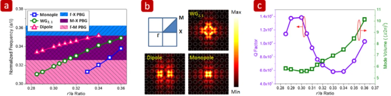
Scheme of our proposed square-PhC point-shifted D0 nanocavity design is shown in Fig. 5. The square-PhCs are defined by air holes on a suspended dielectric slab. The positions and radii r of four central air holes are shifted outward and shrunk to be r’, respectively, to form the nanocavity region. We perform 3D FDTD simulations to investigate the defect modes in this nanocavity. In simulation, the lattice constant, slab thickness, r/a, and r’/a ratio are set to be 500 nm, 220 nm, 0.38, and varied from 0.285 to 0.36, respectively. From the simulation results, three defect modes exist in D0 nanocavity with different r’/a ratios, including WG, dipole, and monopole modes. The relationships between the simulated defect mode frequency and r’/a ratio of square-PhC D0 nanocavity are shown in Fig. 6a. The simulated mode profiles in electrical fields are shown in Fig. 6b. Owing to the potential of WG mode in electrically-driven nanolasers based on nano-post structure, we optimize the Q factor and mode volume of WG mode under different r’/a ratios. As we can see in Fig. 6c, the maximum Q ~ 14,000 and minimum mode volume ~ 5.5(λ/2n)3 (~ 0.065 μm3) are both obtained when r’/a = 0.30. It should be noted that the WG mode volume in this D0 nanocavity design is even smaller than that in square-PhC D1 nanocavity (~ 6.5(λ/2n)3, ~ 0.078 μm3) under the same simulation setup. And the calculated Purcell factor of WG mode under this r’/a ratio is around 1,500.
Top- and tilted-view SEM pictures of fabricated square-PhC D0 nanocavity are shown in Fig. 7a. From nanocavity with fabricated a = 500 nm, r/a ~ 0.38, and r’/a = 0.30, we obtain single-mode lasing at 1560 nm, which can be identified as WG mode by comparing with
7
Fig. 5: Scheme of square-PhC D0 nanocavity on a suspended dielectric slab.
Fig. 6: (a) Plot of FDTD simulated defect mode frequency versus r’/a ratio in square-PhC D0 nanocavity under fixed r/a ratio = 0.38, including WG, dipole, and monopole modes. (b) FDTD simulated mode profiles in electric field of the three defect modes. (c) The simulated Q factor and mode volume of WG mode in D0 nanocavity under different r’/a ratios.
the simulation results in Fig. 6a. The measured light-in light-out (L-L) curve and spectrum of single-mode lasing action are shown in Figs. 7b and 7c. The threshold is estimated to be 160 μW (only 8W is absorbed by the MQWs) from L-L curve. This low threshold is attributed to the small mode volume and high Q factor of WG mode in D0 nanocavity, which directly indicates the potential in achieving thresholdless nanolasers. We also obtain the spectrum below threshold, as shown in the inset of Fig. 7b. The estimated spectral line width by Lorentzian fitting is 0.38 nm, which corresponds to a Q factor of 4,100. And the measured side-mode suppression-ratio is larger than 20 dB as shown in the inset of Fig. 7c.
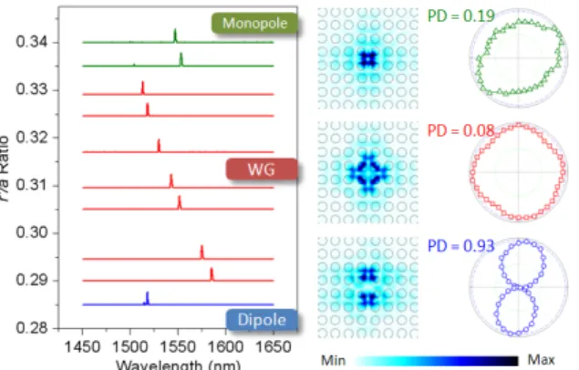
To observe and identify the three modes in experiments, we fabricate a square-PhC D0 nanocavity array with increased r’/a ratio from 0.285 to 0.34. And the measured single-mode lasing wavelengths with different r’/a ratios of the D0 nanocavity are shown in Fig. 8. Compared with the simulation results in Fig. 6a, when r’/a ratio decreases, we can identify the lasing modes from top to bottom in Fig. 8 as monopole, WG, and dipole modes. To further confirm this identification, we measure their polarizations, as shown in Fig. 8. For the identified dipole mode, we obtain a high polarized degree (PD) of 0.93 and observe its wavelength splitting due to degeneracy breaking caused by the fabrication imperfection. On the other hand, WG and monopole modes both show low PD values of 0.08 and 0.19, respectively, because of the far-field cancellations of x- and y-electrical fields. Thus, we can confirm the mode identification.
8
Fig. 7: (a) Top- and titled-view SEM pictures of fabricated square-PhC D0 nanocavity. (b) The measured L-L curve and (c) lasing spectrum of WG mode from square-PhC D0 nanocavity. The measured WG mode spectrum below threshold and the lasing spectrum in logarithm scale are shown in the insets of (b) and (c).
Fig. 8: The relationship between the measured single-mode lasing wavelength and r’/a ratio of square-PhC D0 nanocavity. The simulated mode profiles in electrical fields and measured polarizations of monopole, WG, and dipole modes are also shown.
(II) Protein Adsorption Detection from Modes in PhC D0 Nanocavity
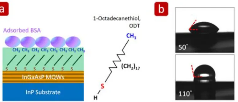
To apply our proposed D0 nanocavity for protein sensing, first, we make a chemical treatment on InGaAsP surface to provide a linking layer at the organic/inorganic interface by 1-octadecanethiol (ODT, HS(CH2)17CH3), as shown in Fig. 9a. Once the linking layer is formed on the InGaAsP surface (can be judged from the surface contact angles shown in Fig. 9b), the protein (bovine serum albumin, BSA) can be adsorbed on the nanocavity surface, as illustrated in Fig. 9a.
The square-PhC D0 nanocavities with different r’/a ratios are treated by above process. The ODT-treated D0 nanocavities are optically pumped by fixed power of 0.6 mW at room temperature and single-mode lasing wavelengths of each defect mode are recorded before and after BSA adsorption. The measured spectra are shown in Fig. 10a. The monopole, WG, and dipole modes show red shifts of 2.0, 1.8, and 1.2 nm in wavelength, respectively, which are arisen from the adsorbed protein on the D0 nanocavity. To further confirm these observations, we apply 3D FDTD method to simulate the wavelength shifts of each mode. We assume the protein adsorbs on the entire surface of the D0 nanocavity. The adsorbed protein is assumed to be with refractive index of 1.5 and its effective thickness is varied
9
Fig. 9: (a) Scheme of protein adsorption on ODT-treated InGaAsP surface. (b) Measured contact angles of oxide-free InGaAsP surfaces before and after ODT treatment, which are 50° and 110°, respectively.
Fig. 10: (a) The measured single-mode lasing spectra of monopole, WG, and dipole modes before (solid-line) and after (bold solid-line) the protein (BSA) adsorption. (b) 3D FDTD simulated wavelength shifts of monopole, WG, and dipole modes (from top to bottom) contributed from the adsorbed protein on the entire D0 nanocavity surface.
from 0 to 2 nm. The simulated results are shown in Fig. 10b. By matching the measured results with the simulated ones, we can obtain an effective protein thickness of 1.55 nm. Considering the defect mode field distribution of only four-lattice-period distance from the
D0 nanocavity, the interrogated analyte amount can be less than 2.2 fg. Furthermore, when we consider the spectral line width of the lasing mode, for example, 0.6 nm for WG mode, the minimum measurable protein amount is less than 0.8 fg, which indicates the high sensitivity of our device. The bio-materials are prepared by Ms. Mong-Ting Lien and Prof. Jui-Chou Hsu (徐瑞洲) from Institute of Molecular Medicine, National Tsing-Hua University, Taiwan.
(III) Spectrum-Free Detection of Nano-Particle by PhC D0 Nanocavity
As we can see in Fig. 8, WG mode shows a very low PD value due to the electric field cancellation in the far field. In reality, this low-polarized property can be broken by deliberate designs or fabrication non-uniformities and the WG mode will become polarized. In our devices, we observe this modal symmetry breaking due to a dielectric nano-particle (NP) nearby the nanocavity. Here, we compare the WG mode lasing actions from square-PhC D0 nanocavities with and without a 350 nm-diameter dielectric NP nearby, as shown in Fig. 11a. From measured polarizations in Fig. 11b, obviously, the PD increases to
10
Fig. 11: (a) Top-view SEM pictures of square-PhC D0 nanocavities (top) without and (bottom) with a 350 nm NP nearby. The measured (b) polarizations and (c) L-L curves of WG mode in square-PhC D0 nanocavities with and without a NP nearby.
be 0.69 when there is a NP nearby the nanocavity. This strong influence is attributed to the comparable sizes between D0 nanocavity and the NP. The measured L-L curves of these two cases are shown in Fig. 11c. The slope efficiency increases significantly when the NP is presented. This is because when the NP breaks the modal symmetry of WG mode, it also breaks the WG modal cancellation in the far field. Thus, there will be more radiation components collected by the objective lens and lead to the increased slope efficiency. This observed unique behavior of WG mode based on polarization variation could be a spectrum-free approach to detect NPs. That means the requirement of very high Q factors in PhC nanocavities by very delicate modulations is not essential for detection down to single molecule binding or attaching via this approach, which is potential in bio-chemical or drug discovery researches after further investigations.
III. P
HC
M
ICROCAVITIES FORO
PTICALLYS
ENSINGS
TRESSSo far, we have demonstrated the optical index and NP sensors based on PhC micro- and nano-cavities. Optical stress sensor is another important component in mechanical and semiconductor applications, especially in optical micro-electromechanical systems. Although some interesting optical stress sensor designs based on PhCs or PhC waveguides have been reported, the designs based on high Q micro- or nano-cavities are still hard to find in literatures and the sensitivity of present designs can be further improved. In this section, we will briefly illustrate the design principles of a highly sensitive optical stress sensor. According to the requirements, we introduce a structural design composed of doubled-layered (DL) PhC microcavity. The basic modal properties, structural variations, and corresponding optical spectrum response of DL PhC microcavity are investigated by 3D FDTD and finite-element method (FEM) simulations.
11
(I) Design Principle for Optically Sensing Stress by PhC Microcavity
First, for a designed stress sensor structure, we should find the relationship between the applied stress and the corresponding structural variation. And then the relationship between the structural variation and the corresponding wavelength shift should be figured out. According to these two relationships, we can estimate the applied stress by the measured optical spectrum shift and decide how small the detectable stress variation per wavelength unit (in newton unit per optical wavelength shift in nanometer, N/nm) is. Furthermore, we can exactly define the minimum detectable stress variation (δF, in newton unit) by considering the minimum spectral line width of the measured light wave. Thus, we can define a simple equation to illustrate this relationship:
SWQ Q d d F F λ λ λ δ × = Δ Δ × Δ Δ = (1) where ΔF / Δd and Δd / Δλ represent the applied stress needed to cause specific structural variation and the structural variation needed to cause specific wavelength shift, respectively. From equation (1), we find the highly sensitive optical stress sensor can be achieved by small ΔF / Δd and Δd / Δλ. In addition, high Q factor of the microcavity is also necessary to achieve small δF. For simplicity, we define factors of S = Δd / ΔF and W = Δλ / Δd to represent the structural variation rate due to the applied stress and wavelength shift rate due to the structural variation, respectively. And the δF can be expressed as λ / SWQ in equation (1).
(II) Modal Properties of Double-Layered PhC Microcavities and its Stress Sensing Application
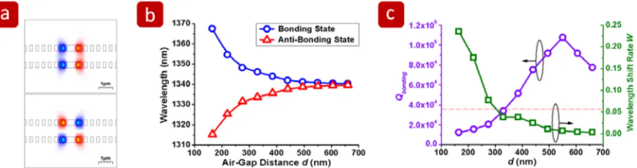
In our previous works, we have proposed a PhC CD2 microcavity design, which can sustain a high Q WG mode, as shown in the insets of Fig. 12. Based on this microcavity design, we propose a novel DL PhC microcavity structure composed by two identical PhC
CD2 microcavity slabs, as shown in Fig. 12. By using 3D FDTD simulation, we obtain bonding and anti-bonding modes in DL PhC microcavity and their mode profiles in electric field are shown in Fig. 13a. The relationships between wavelengths of bonding and anti-bonding modes and air-gap distance are shown in Fig. 13b. We investigate the Q variation of bonding mode under different gap distance d, which is shown in Fig. 13c. We obtain a high enhanced Q of 110,000 when d = 550 nm. We also show W factors under different d in Fig. 13c. Although the highest Q is available when d = 550 nm, the W factor at this d value is smaller than the cases with smaller d. Since the δF in equation (1) depends both on the Q and W factors, we can conclude there will be a trade-off between the Q and W factors for small δF.
12
Fig. 12: Scheme of DL PhC CD2 microcavity design. The microcavity design and the simulated WG mode profile in electric-field are shown in the right insets A and B.
Fig. 13: (a) The simulated mode profiles in electric-field in x-z plane of bonding (top) and anti-bonding (bottom) modes. (b) The simulated wavelengths of bonding and anti-bonding modes versus the air-gap distance d. (c) The simulated Q and W factors of bonding mode for d varied from 165 to 660 nm.
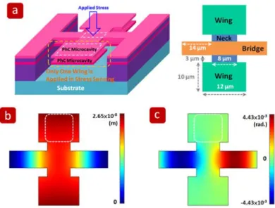
So far, we have obtained the Q and W factors of DL PhC microcavity. To obtain the S factor in equation (1), we present a geometry named bridge-with-wings (BwWs) for DL PhC microcavity, as shown in Fig. 14a. In this BwWs geometric design, the PhC microcavity and the point stress are defined and applied on the wing and bridge regions, respectively. The separation of stress applying region (bridge) and sensing region (wings, PhC microcavities) guarantees the uniform displacement between the double layers when a stress is applied. The FEM simulated air-gap displacement Δd and torsion distribution when
F = 50 nN are shown in Figs. 14b and 14c. In Fig. 14b, the maximum Δd is 3.3 nm in the
PhC region, which corresponds to non-uniformity of 6.6 %. In addition, in Fig. 14c, the torsion mainly distributes in the bridge region and is close to zero in the wing region. This also indicates the x-y elongation in the PhC region due to torsion can be ignored in this design. From the FEM simulation results of BwWs geometry, we obtain the relationship between the applied stress F and the air-gap displacement Δd, as shown in Fig. 15a. The calculated structural variation rates S of the BwWs geometry are 0.507 and 0.229 nm/nN for InGaAsP and silicon materials, respectively. We should note that the S factors using silicon material are twice smaller than those using InGaAsP, which means twice structural response for applied stress by using InGaAsP instead of silicon under the same geometric design.
13
Fig. 14: (a) Scheme of DL PhC microcavity in BwWs geometry. The simulated (b) air-gap displacement Δd and (c) torsion distribution of the InGaAsP BwWs geometry when F = 50 nN.
Fig. 15: (a) The simulated relationship between the applied stress and air-gap displacement Δd. The relationships of BwWs geometry for silicon and InGaAsP materials are presented. (b) The calculated minimum detectable stress variation δF for the BwWs geometry under different air-gap distance d.
According to equation (1) and combining FEM and FDTD simulation results, we can obtain δF of BwWs geometry when d = 165 - 660 nm, as shown in Fig. 15b. The smallest
δF is only 0.95 nN when d = 165 nm. We also find that the δF can be maintained nearly
constant at a low value around 1 to 2 nN under a large range of initial d (165 - 440 nm) as indicated by the shadow region in Fig. 15b, which provides a large design and fabrication tolerances in keeping high sensitivity. Thus, we believe this DL PhC microcavity is potential and promising in demonstrating ultra-high sensitivity optical stress sensors.
14
Achievement Summary
The main goals of original proposal and our achievements are summarized below:I. PhC-Based Optical Index and Bio-Sensors
z We theoretically propose and experimentally demonstrate a PhC HSE microcavity laser that can sustain a high Q (~ 6.6 x 10⁵) surface mode.
Related Publication: “Photonic crystal hetero-slab-edge microcavity with high quality factor surface mode for index sensing,” Appl. Phys. Lett. 94, 141110 (2009). (SCI IF: 3.726) (Cited: 2)
z We set up a gas index measurement system and confirm the high index response of 625 nm/RIU from surface mode via detecting CO2 gas under different gas pressures. Very small detectable index variation of 4 × 10⁻⁴ is achieved.
Related Publication: “High Index Sensitivity of Surface Mode in Photonic Crystal Hetero-Slab-Edge Microcavity,” Opt. Lett. 35, pp. 1452-1454 (2010). (SCI IF: 3.772)
z We propose and demonstrate an ultra-small nanocavity laser based on square-PhCs, which is potential in electrically-driven thresholdless nanolaser source. Ultra-low threshold of 8 μW is obtained from WG mode lasing. We also propose and demonstrate a spectrum-free approach for detecting nano-particle via WG mode polarization variation in this D0 nanocavity.
Related Publication: “Square lattice photonic crystal point-shifted nanocavity with lowest-order whispering-gallery mode,” Opt. Express 18, pp. 2566-2572 (2010). (SCI IF: 3.880) (Cited: 1) (Also Selected for Virtual Journal of Biomedical Optics, Vol. 5, issue 4, Feb. 26, 2010))
z We experimentally identify all defect modes in square-PhC D0 nanocavity laser. By specific functionalized surface treatment by ODT, we successfully observe the optical responses of defect modes owing to the protein adsorption on the nanocavity surface. Effective adsorbed protein thickness of 1.55 nm is obtained. Very small detectable protein mass of 0.8 fg (~ 7,300 BSA molecules) is achieved.
Related Publication: “Optical sensing of square lattice photonic crystal point-shifted nanocavity for protein adsorption detection,” Appl. Phys. Lett. 96, 213702 (2010). (SCI IF: 3.726)
II. PhC-Based Optical Stress Sensor
z We propose a novel DL PhC microcavity for highly sensitive optical stress sensor in simulations. We illustrate the design principle, and investigate modal and structural properties of DL PhC microcavity by FDTD and FEM simulations. We obtain a very small minimum detectable stress variation δF of 0.95 nN and a large design tolerance with constant δF around 1 to 2 nN.
Related Publication: “Ultra-high sensitivity optical stress sensor based on double-layered photonic crystal microcavity,” Opt. Express 17, pp.1518-1526 (2009). (SCI IF: 3.880) (Cited: 2)
15
Future Work for the 2
ndYear Project
In the 1st year, we have shown the possibilities and potentials of PhC nanocavitiesserving as highly sensitive optical sensors. Index, nano-particle, protein adsorption, and stress sensors have been investigated in simulations and experiments. According to present achievements, for the 2nd year, we will make efforts on the following issues:
z Although we have initially demonstrated index sensor by PhC HSE microcavity, slab-edge termination, lattice structure, and cavity length have not been optimized yet. In the 2nd year, we expect the experimental minimum detectable index variation can be further improved to the level of 10-5.
z We have demonstrated protein adsorption sensing with molecular level sensitivity by a novel PhC ultra-small D0 nanocavity. In the 2nd year, we expect sensing specific binding between molecules or anti-gen/anti-body by PhC nanocavity can be achieved. We will also investigate the possibility of sensitivity down to single molecule by PhC nanocavity both in simulation and experiment. (In the 2nd year, Ms. Lien and Prof. Hsu will continue their kind assistance in preparing various bio-materials and provide fruitful discussions.)
z Although we have proposed and demonstrated a spectrum-free approach to detect a nano-particle, there are lots of possibilities to develop such user-friendly detection tools. Thus, we will also make efforts on nano-particle manipulation and detection based on PhC defect devices, which would be very important tools in bio-medical research.
z In the 1st year, we have exhaustively investigated the DL PhC microcavity in simulations for highly sensitive optical stress sensors. Based on present design, we expect we can realize it in the 2nd year.
16
Publications during the 1
stYear Project Period (2009 - Present)
From 2009 to present, we have published 12 papers on famous international journals and
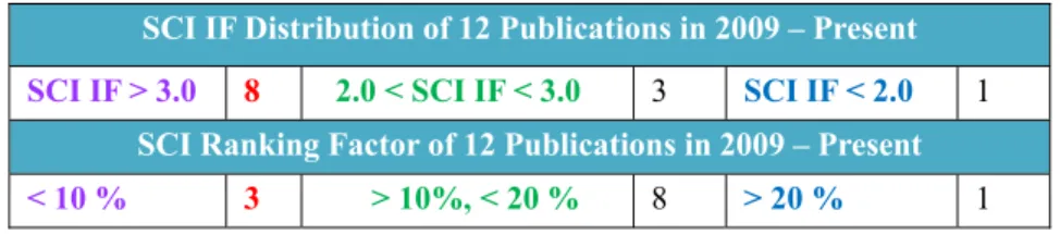
letters, including Optics Express (2008 SCI IF: 3.880), Optics Letters (2008 SCI IF: 3.772), Applied Physics Letters (2008 SCI IF: 3.726), and so on. We also give oral and poster presentations in very famous international conferences, including CLEO, MRS, and OSA Topical Meeting. The statistics and details of SCI IF and ranking factor of our publications are shown in Table II. The detailed publication list is also provided below.
Table II: The SCI IF, ranking factor, and citing number of our publications (2009 - present).
SCI IF Distribution of 12 Publications in 2009 – Present SCI IF > 3.0 8 2.0 < SCI IF < 3.0 3 SCI IF < 2.0 1
SCI Ranking Factor of 12 Publications in 2009 – Present < 10 % 3 > 10%, < 20 % 8 > 20 % 1
Publication List (2009 - Present)
(I) International Letter & Journal Articles (Based on 2008 SCI IF)
1. Tsan-Wen Lu, Pin-Tso Lin, Kuan-Un Sio, and Po-Tsung Lee, “Optical sensing of square lattice photonic crystal point-shifted nanocavity for protein adsorption detection,” Appl. Phys. Lett. 96, 213702 (2010). (SCI IF: 3.726) 2. Tsan-Wen Lu, Yi-Hua Hsiao, Wei-De Ho, and Po-Tsung Lee, “High Index Sensitivity of Surface Mode in Photonic
Crystal Hetero-Slab-Edge Microcavity,” Opt. Lett. 35, pp. 1452-1454 (2010). (SCI IF: 3.772)
3. Tzu-Yueh Chang, You-Wei Cheng, and Po-Tsung Lee, “Electrical characteristics of an organic bistable device using an Al/Alq3/nanostructured MoO3/Alq3/p+-Si structure,” Appl. Phys. Lett. 96, 043309 (2010). (SCI IF: 3.726) 4. Tsan-Wen Lu, Pin-Tso Lin, Kuan-Un Sio, and Po-Tsung Lee, “Square lattice photonic crystal point-shifted
nanocavity with lowest-order whispering-gallery mode,” Opt. Express 18, pp. 2566-2572 (2010). (SCI IF: 3.880)
(Cited: 1)(Selected for Virtual Journal of Biomedical Optics, Vol. 5, issue 4, Feb. 26, 2010)
5. Wei-De Ho, Tsan-Wen Lu, Yi-Hua Hsiao, and Po-Tsung Lee, “Thermal Properties of 12-Fold Quasi-Photonic Crystal Microcavity Laser with Size-Controlled Nano-Post for Electrical Driving,” J. Lightwave Technol. 27, pp. 5302-5307 (2009). (SCI IF: 2.736) (Cited: 1)
6. Chia-Ho Chen, Tsan-Wen Lu, and Po-Tsung Lee, “Microcavity Laser Emissions Based on Double Hetero-Structure by Locally Modulated Photonic Crystal Waveguide,” J. Lightwave Technol. 27, pp. 4393-4400 (2009). (SCI IF: 2.736)
7. Ming-Feng Chang, Po-Tsung Lee, and Albert Chin, “Low Threshold Voltage MoN/HfAlO/SiON p-MOSFETs with 0.85-nm EOT,” IEEE Electron. Device Lett. 30, pp. 861-863 (2009). (SCI IF: 3.049) (Cited: 1)
8. Tsan-Wen Lu, Yi-Hua Hsiao, Wei-De Ho, and Po-Tsung Lee, “Photonic crystal hetero-slab-edge microcavity with high quality factor surface mode for index sensing,” Appl. Phys. Lett. 94, 141110 (2009). (SCI IF: 3.726) (Cited: 2)
9. Albert Chin, Ming-Feng Chang, S. H. Lin, W. B. Chen, Po-Tsung Lee, F. S. Yeh, C. C. Liao, M. F. Li, N. C. Su and S. J. Wang, "Flat Band Voltage Control on Low Vt Metal-Gate/High-κ CMOSFETs with small EOT," Microelectron.
Eng. 86, pp. 1728-1732 (2009).(SCI IF: 1.503)
10. Hsiao-Wen Zan, Cheng-Wei Chou, Chung-Hwa Wang, Ho-Tsung Song, Jenn-Chang Hwang, and Po-Tsung Lee, "Carbon Attachment on the Aluminum Nitride Gate Dielectric Pentacene Based Organic Thin Film Transistors," J.
Appl. Phys. 105, 063718 (2009).(SCI IF: 2.201) (Cited: 1)
11. Tsan-Wen Lu and Po-Tsung Lee, “Ultra-high sensitivity optical stress sensor based on double-layered photonic crystal microcavity,” Opt. Express 17, pp.1518-1526 (2009).(SCI IF: 3.880) (Cited: 2)
17
12. Ming-Feng Chang, Po-Tsung Lee, S. P. McAlister, and Albert Chin, “Small Sub-threshold-Swing and Low-Voltage, Flexible Organic Thin Film Transistors which use HfLaO as the Gate Dielectric,” IEEE Electron.
Device Lett. 30, pp.133-135 (2009).(SCI IF: 3.049) (Cited: 4)
(II) International Conference Presentations
1. Pin-Tso Lin, Tsan-Wen Lu, and Po-Tsung Lee, “All-optical Controlled-transport Of Nanoparticles On Wedge-shaped Photonic Crystal Waveguides,” IWB4, OSA IPR’10, Monterey, California, USA (2010).
2. Tsan-Wen Lu, Pin-Tso Lin, Kuan-Un Sio, and Po-Tsung Lee, “Square Lattice Photonic Crystal Point-Shifted D0 Nanocavity with Lowest-Order Whispering-Gallery Mode,” CWK5, IEEE/OSA CLEO/QELS’10, San Jose, California, USA (2010).
3. Yi-Heng Tsai, Yi-Shian Lin, Tzu-Yueh Chang, and Po-Tsung Lee, “Annealing Condition Dependent Room Temperature PL of Si Nano-crystals Thin Film,” T10.32, 2010 MRS Spring Meeting, San Francisco, California, USA (2010).
4. You-Wei Cheng, Tzu-Yueh Chang, and Po-Tsung Lee, “Characteristics of Organic Memory Using Metal Oxide Nano-clusters,” G17.3, 2010 MRS Spring Meeting, San Francisco, California, USA (2010).
5. Yi-Hua Hsiao, Tsan-Wen Lu, Wei-De Ho, and Po-Tsung Lee, “High-Q Photonic Crystal Hetero-Slab-Edge Microcavity Laser for Index Sensing,” IEEE/OSA CLEO/QELS’09, CTuDD4, Baltimore, Maryland, USA (2009). 6. Wei-De Ho, Yi-Hua Hsiao, Tsan-Wen Lu, and Po-Tsung Lee, “Thermal Properties of Post-Size Controlled 12-Fold
Quasi-Photonic Crystal Microcavity for Electrically-Driving,” IEEE/OSA CLEO/QELS’09, CFE4, Baltimore, Maryland, USA (2009).