國 立 交 通 大 學
機械工程學系
博 士 論 文
奈秒脈衝Nd:YAG雷射系統於光電材料
表面製程之應用與研究
Application and Study on Surface Process of Optoelectric
Materials by a Nanosecond Pulsed Nd:YAG Laser System
研 究 生:曾釋鋒
指導教授:周長彬 教授
奈秒脈衝
Nd:YAG 雷射系統於光電材料表面製程之應用與研究
Application and Study on Surface Process of Optoelectric Materials by a
Nanosecond Pulsed Nd:YAG Laser System
研 究 生:曾釋鋒 Student:Shih-Feng Tseng
指導教授:周長彬 Advisor:Chang-Pin Chou
國 立 交 通 大 學
機 械 工 程 學 系
博 士 論 文
A DissertationSubmitted to Department of Mechanical Engineering College of Engineering
National Chiao Tung University in partial Fulfillment of the Requirements
for the Degree of Doctor of Philosophy in Mechanical Engineering September 2011 Hsinchu, Taiwan
中華民國 一百 年 九 月
i
奈秒脈衝 Nd:YAG 雷射系統於光電材料表面製程之應用與研究
研究生:曾釋鋒
指導教授
:周長彬 教授
國立交通大學機械工程學系
摘要
近年來透明導電材料、非球面玻璃透鏡和高複雜形狀玻璃基板廣泛應用於 3C 商品 (如電腦、通訊和消耗性電子產品),以滿足光電和半導體產業迅速發展。為了要增加生 產速度、降低生產設備沈重投資和減少對環境化學傷害,目前微奈米雷射製程紛紛被廣 泛使用,其技術包括雷射剝蝕、雷射銑削、雷射退火、雷射刻紋、雷射處理、雷射沈積 等。新穎雷射直寫和雷射背寫技術也被開發應用於材料表面製程。 本研究目的係使用奈秒脈衝 Nd:YAG 雷射系統發展材料表面製程技術應用於光電 產業,並瞭解雷射與材料加工之間交互作用關係。在觸控面板電極絕緣研究方面,使用 1064 nm 波長之 Nd:YAG 雷射於氧化銦錫薄膜進行劃線,其薄膜分別鍍製於鈉鈣玻璃 (Soda-lime glass)、聚碳酸酯(PC)和環烯烴共聚物(COC)三種不同基板上,薄膜厚度分別 為 20 nm、30 nm 和 20 nm。最大雷射功率固定在 2.2 瓦,調整雷射照射時間從 10 μs 到 100 μs,探討薄膜劃線後寬度、深度和導電特性。另外,藉由掃描式電子顯微鏡、三維 共焦雷射掃描顯微鏡、原子力顯微鏡和四點探針量測薄膜表面形貌、表面交互作用、表 面粗糙度、光學性質和導電性質。雷射劃線後氧化銦錫薄膜表面形貌量測結果顯示:當 雷射照射時間在 10 μs 和 20 μs 時,雷射劃線路徑上仍有殘留氧化銦錫薄膜;當雷射照 射時間在 30 μs 到 60 μs 間,可獲得較佳品質之雷射劃線;當雷射照射時間大於 60 μs 時, 聚碳酸酯(PC)和環烯烴共聚物(COC)塑膠基板上雷射劃線薄膜會產生局部燒焦區域,且 當雷射照射時間增加時,絕緣線寬度和薄膜電阻率也隨之增加。 矽基板表面粗糙圖案製程研究方面,係調整脈衝 Nd:YAG 雷射不同能量密度和脈衝 作用時間,探討表面刻紋之微結構與表面粗糙度。掃描式電子顯微鏡和三維共焦雷射掃ii 描顯微鏡分別用於量測雷射表面刻紋後之矽基板表面微形貌和表面粗糙度,FTA 188 接 觸角量測分析儀用於液珠與刻紋基板間接觸角量測。實驗結果指出:增加雷射密度和雷 射脈衝作用時間,使得較多熔渣堆積在這些圖案周圍而形成微火山口,且會增加火山口 高度和表面粗糙度。水滴在雷射刻紋後矽基板表面之典型例子顯示:水滴非常迅速攤 開,幾乎在 0.5167 秒內就完全消失不見;相較於水滴在未經過雷射刻紋處理之表面,其 接觸角為 47.9 度。另外,脈衝 Nd:YAG 雷射搭配雷射誘發背寫製程和雷射誘發電漿輔 助剝蝕技術,用於鈉鈣玻璃表面加工粗糙陣列圖案。實驗結果顯示:隨雷射加工次數和 單發雷射曝曬時間增加,加工後表面形成之火山口高度和深度也會增加。接著在雷射背 寫加工後玻璃表面鍍製一層 695 nm 鐵氟龍薄膜後,其表面變成疏水特性。水滴在玻璃 基板鍍製鐵氟龍薄膜表面之典型例子顯示:其水滴接觸角為 118.6 度;當水滴在環形溝 槽樣板鍍製一層鐵氟龍薄膜,其水滴接觸角提高至 131.3 度。 Nd:YAG 雷射表面處理技術應用於玻璃模造模仁保護膜方面研究,係使用離子源輔 助磁控濺鍍系統鍍製不同合金薄膜成分,包括鉑(25%)-銥、鉑(50%)-銥、鉑(75%)-銥、 鎳(25%)-銥、鎳(50%)-銥和鎳(75%)-銥合金。在合金薄膜與碳化鎢模仁表面間鍍製一層 鉻膜當作緩衝層,接著 Nd:YAG 雷射直接應用於表面處理製程,探討合金膜於高溫環境 下之表面性質。在雷射表面處理 1500℃後,當鉑和鎳成分增加時,表面粗糙度也隨之增 加。因薄膜受到高溫工作環境而產生氧化,這些薄膜表面是較粗糙、低微硬度和低彈性 模數。因此,建議這些銥合金薄膜在真空環境和填充保護氣體操作對玻璃模造製程是有 益的,可避免嚴重表面氧化和降低表面粗糙度值。 關鍵字:脈衝 Nd:YAG 雷射、電極絕緣、雷射劃線、氧化銦錫薄膜、表面刻紋技術、接 觸角、雷射誘發背寫、雷射誘發電漿輔助剝蝕、鐵氟龍薄膜、保護膜、鉑-銥合金、鎳-銥合金、表面處理、玻璃模造模仁、表面氧化
iii
Application and Study on Surface Process of Optoelectric
Materials by a Nanosecond Pulsed Nd:YAG Laser System
Student:Shih-Feng Tseng
Advisors:Prof. Chang-Pin Chou
Department of Mechanical Engineering
National Chiao Tung University
ABSTRACT
In recent years, transparency conductive materials, aspheric glass lenses, and glass plates of highly complex shape with fine edges were extensively used in 3C market products (i.e. computer, communication, and consumer electronics) to meet the rapid development of the electro-optical and semiconductor industry. In order to increase the processing speeds, to reduce the heavy investment of the processing equipment, and to decrease the chemical harm to the environment, current laser micro- or nano-machining processes employ techniques including laser ablation, laser milling, laser annealing, laser texturing, laser treatment, laser deposition, etc. Moreover, novel techniques, laser direct writing and laser backside writing methods, are also developed to use in the surface process of materials.
The purposes of this dissertation aim to develop the surface processing techniques on materials used for the optoelectric applications by a nanosecond pulsed Nd:YAG laser system and to better understand the interaction between laser beam and materials. In the electrode isolation for touch panels, the Nd:YAG laser with wavelength of 1064 nm is used to scribe the indium tin oxide (ITO) thin films coated on three types of substrate materials, i.e. soda-lime glass, polycarbonate (PC), and cyclic-olefin-copolymer (COC) materials with thickness of 20 nm, 30 nm, and 20 nm, respectively. The effect of exposure time adjusted from 10 μs to 100 μs on the ablated mark width, depth, and electrical properties of the scribed film was investigated. The maximum laser power of 2.2 watts was used to scribe these thin films. In addition, the surface morphology, surface reaction, surface roughness, optical properties, and electrical conductivity properties were measured by a scanning electron
iv
microscope, a three-dimensional confocal laser scanning microscope, an atomic force microscope, and a four-point probe. After laser scribing, the measured results of surface morphology show that the residual ITO layer was produced on the scribed path with the laser exposure time at 10 μs and 20 μs. The better edge qualities of the scribed lines can be obtained when the exposure time extends from 30 μs to 60 μs. When the laser exposure time is longer than 60 μs, the partially burned areas of the scribed thin films on PC and COC substrates are observed. Moreover, the isolated line width and resistivity values increase when the laser exposure time increases.
In a surface-texturing technique to create rough patterns on a silicon substrate by the pulsed Nd:YAG laser system, the different degrees of microstructure and surface roughness were adjusted by the laser fluenceand laser pulse duration. A scanning electron microscope (SEM) and a 3D confocal laser scanning microscope are used to measure the surface micrograph and roughness of the patterns, respectively. The contact angle variations between droplets on the textured surface were measured using an FTA 188 video contact angle analyzer. The results indicate that increasing the values of laser fluence and laser pulse duration pushesmore molten slag piled around these patterns to create micro-sized craters and leads to an increase in the crater height and surface roughness. A typical example of a droplet on a laser-textured surface shows that the droplet spreads very quickly and almost disappears within 0.5167 s, compared to a contact angle of 47.9° on an untextured surface. In addition, the pulsed Nd:YAG laser is also utilized to fabricate rough array-patterns on a soda-lime glass plate by a laser-induced backside writing (LIBW) process and a laser-induced plasma assisted ablation (LIPAA) technique. The measured results show that crater height and depth gradually increases with increasing number of passes and single-shot laser exposure time. After a 695 nm thick Teflon thin film is deposited on the glass plate, the micro-machined template surfacebecomes hydrophobic. The typical measured contact angle on a planar glass substrate coated with Teflon is 118.6°. The contact angle increases to 131.3° when the water drop is added on a round annular-grooved template coated with Teflon.
In the Nd:YAG laser surface treatment technology for the protective coatings of glass-molding dies, a variety of alloy films, including Ir-25 at.% Pt, Ir-50 at.% Pt, Ir-75 at.% Pt, Ir-25 at.% Ni, Ir-50 at.% Ni, and Ir-75 at.% Ni compositions are deposited by the ion source assisted magnetron sputtering system (ISAMSS). A Cr layer that functioned as a buffer layer is deposited between the alloy film and die surface. After an alloy film and the buffer Cr layer were sequentially coated on tungsten carbide (WC) surface, Nd:YAG laser was directly
v
applied in the surface treatment process. The temperature profile of the film stacks structure is simulated by ANSYS software. After laser surface treatment at 1500℃, the values of surface roughness are obviously increased as increasing concentrations of Pt or Ni. These surface films are high roughness, low microhardness and low reduced modulus because of the film oxidation occurred in high working temperature process. Therefore, these Ir-alloy coatings operated under the vacuum environment and filled with protective gas are useful in glass molding to avoid the severe surface oxidation and to reduce surface roughness.
Keywords: Pulsed Nd:YAG laser, electrode isolation, laser scribing, indium tin oxide (ITO)
thin films, surface-texturing technique, contact angle, laser-induced backside writing (LIBW), laser-induced plasma assisted ablation (LIPAA), Teflon thin film, protective coatings, Pt-Ir alloy, Ni-Ir alloy, surface treatment, glass-molding die, surface oxidation.
vi
誌謝
感謝指導教授周長彬博士在我博士班就讀期間的悉心指導與關懷,使學生在雷射加 工與材料分析專業領域受益良多,且順利完成博士論文研究。師恩浩瀚,永銘我心,特 誌卷首,謹致上衷心之謝忱。 感謝交通大學機械系鄭璧瑩副教授、台北科技大學機械系湯華興教授、彰化師範大 學機電系陳明飛教授和國研院儀器科技研究中心黃國政博士,撥冗擔任博士論文口試委 員,並於口試過程中提供寶貴意見及斧正,使論文內容能更臻完整。 感謝國研院儀器科技研究中心蔣東堯博士和蕭文澤博士,對於研究期間給予論文指 導與討論,使論文發表更加順利。感謝儀科中心同事李昭德博士、陳維鈞先生、蘇健穎 先生、朱念南小姐、卓文浩先生、光學廠與機械廠同仁,於研究期間對實驗試片量測與 加工之協助。感謝彰化師範大學機電系陳明飛教授提供 Nd:YAG 雷射實驗設備,感謝龍 華科技大學工程技術研究所丁鯤教授提供奈米壓痕量測儀,及實驗室同學建堯和治豪、 學弟彥彬和治偉在研究期間的協助,使論文得以順利完成,在此,謹致上最誠摯的謝意。 最後,感謝父母、老婆及家人在求學過程中,給予最大的支持與鼓勵,讓我在無後 顧之憂的環境下,全力以赴的完成學業,謹獻上內心無限的感激。 曾釋鋒 謹識 中華民國一百年九月vii
Contents
Abstract (in Chinese)………...i
Abstract (in English)………...iii
Acknowledgements (in Chinese)………vi
Contents………vii
Table captions………..x
Figure captions………...ix
Chapter 1 Introduction………1
1.1 Backgrounds………....1
1.1.1 Electrode forming of TCO thin films………...3
1.1.2 Wettability of material surfaces………5
1.1.3 Hard coatings for glass-molding dies………...7
1.2 Motivation and objectives………...9
1.3 Structure of the dissertation………..10
Chapter 2 Literatures review……….12
2.1 Laser scribing of TCO thin films………..12
2.2 Wetting effects of various textured surfaces……….18
2.3 Protective coating compositions for glass-molding dies………...26
2.4 Laser treatment technology of material surfaces………..29
Chapter 3 Laser processing mechanisms and parameters……….32
3.1 Laser processing mechanisms………...32
3.1.1 Laser radiation absorption mechanisms……….32
3.1.2 Laser direct writing and laser-induced backside writing………...34
3.2 Laser processing parameters……….36
Chapter 4 Experimental apparatus and sample preparation………..39
4.1 Laser scribing of indium tin oxide (ITO) thin films deposited on various substrates for touch panels………...39
4.1.1 Laser scribing system……….39
4.1.2 Sample preparation………40
4.1.3 Isolation line patterning parameter………45
4.2 Surface wettability of silicon substrates enhanced by laser ablation………45
viii
4.2.2 Surface texting by laser ablation………47
4.2.3 Wettability characteristics of the textured surfaces………48
4.3 Hydrophobic templates with rough patterns fabricated by laser micromachining for liquid droplets generation………..49
4.3.1 Laser micromachining system………...49
4.3.2 Templates made by hydrophobic processes………...50
4.4 Characteristics of Ni-Ir and Pt-Ir hard coatings surface treated by pulsed Nd:YAG laser irradiation……….52
4.4.1 Numerical simulation process………52
4.4.2 Laser surface treatment system………..54
4.4.3Sample preparation……….55
Chapter 5 Experimental results and discussion……….57
5.1 Laser scribing of indium tin oxide (ITO) thin films deposited on various substrates for touch panels………...57
5.1.1 Surface morphology, isolation line width, and depth……….57
5.1.2 Electrical conductivity measurement……….63
5.1.3 Summary………64
5.2 Surface wettability of silicon substrates enhanced by laser ablation………64
5.2.1 Square patterning on silicon substrates………..64
5.2.2Surface morphologies……….65
5.2.3 Surface roughness………..69
5.2.4 Enhanced wettability of liquid droplets on laser textured surfaces………...69
5.2.5 Summary………70
5.3 Hydrophobic templates with rough patterns fabricated by laser micromachining for liquid droplets generation………..71
5.3.1 Surface morphologies of machined templates……….…..71
5.3.2 Surface profiles of machined templates……….73
5.3.3 Contact angle of water droplets on the hydrophobic template………...75
5.3.4 Summary………76
5.4 Characteristics of Ni-Ir and Pt-Ir hard coatings surface treated by pulsed Nd:YAG laser irradiation……….77
5.4.1 SEM observations on different composition alloy films………77
5.4.2 The temperature distribution profile of the different composition alloy films…..77 5.4.3 Description of surface roughness of Pt-Ir and Ni-Ir films treated by laser
ix
annealing………...79
5.4.4 Oxidation analysis using EDS………81
5.4.5 Microhardness and reduced modulus property………..83
5.4.6 Summary………83
Chapter 6 Conclusions and future work………86
6.1 Conclusions………...86
6.2 Future work………...88
References……….89
Vita………98
x
Table captions
Table 4.1 Fundamental Nd:YAG laser system parameters………40 Table 4.2 Optical and electrical properties of ITO film deposited on different substrates …42 Table 4.3 Physical characteristics of Tungsten carbide (WC) mold for glass molding………54 Table 5.1 Machining parameters of the annular groove and measured results………72 Table 5.2 Summarized table of processing parameters for laser treatment………79 Table 5.3 Comparison of surface roughness before and after laser treatment………80
xi
Figure captions
Figure 1.1 Common high-power laser sources for industry ... 2 Figure 1.2 Long-pulse laser matter interaction [1] ... 2 Figure 1.3 Short-pulse laser matter interaction [2] ... 2 Figure1.4Products of touch panel application. (a) Elonex e-Book reader [9] and (b) Apple iPhone [10] ... 3 Figure 1.5 Schematic diagram of fundamental structure for resistive touch panel [11] ... 4 Figure 1.6 Semiconductor processes for patterning electrodes of transparent conductive oxide ... 5 Figure1.7Schematic diagram of a wettable surface [13]. (a) Superhydrophobic surface, (b) hydrophobic surface, and (c) hydrophilic surface ... 6 Figure1.8 Products of surface wettability application [22]. (a) Digital microfluidic biochip and (b) multifunctional biochemical detection biochip system ... 6 Figure 1.9 Pictures of a glass-molding system [23]. (a) Glass-molding machine of Toshiba-GMP207HV and (b) glass-molding die ... 8 Figure 1.10 Flow diagram for glass-molding processes [24] ... 8 Figure 1.11 Application of glass-molding process for fabricating various lenses [24] ... ..9 Figure 2.1 SEM images of Ag/Au pattern (a), Al/Ag pattern (b), edge-peeled Al/Ag stripe pattern fabricated by two-beam interference (c), and micro-tubes formed by furtherincreasing the pulse power (d) [26] ... 13 Figure 2.2 Schematic illustration of high-resolution ITO patterning process [27] ... 14 Figure2.3Optical profiler images of patterned Au (top) and ITO (bottom) films (a) and ITO patterns created using holographically patterned Al layers (b) [29] ... 14 Figure2.4 Ablation depths and widths at different fluences measured by increasing the number of laser pulses [34] ... 15 Figure 2.5 UV laser direct writing of ITO thin films with different feed rates [35] ... 16 Figure 2.6 Schematic diagram of laser beam transmittance [36] ... 17 Figure2.7SEM images of the surface morphology of ablated by the Nd:YAG laser at different overlapping rate: (a) 0%, (b) 25%, and (c) 62% [38] ... 18 Figure 2.8 Pictures of 1 mg water droplets on prepared pillar structures [18] ... 19 Figure2.9Spreading-process images of water droplets with different impact conditions on the hydrophobic grooved surface [40] ... 20 Figure2.10SEM photos of the textured surfaces fabricated by using the standard lithography process, (a) chain-configuration and (b) concentric circular configuration [47] ... 21
xii
Figure 2.11 Dynamic motion of a droplet on a separated route [47] ... 21
Figure 2.12 FESEM images (top), EDX analysis spectra (middle), and water contact angles (bottom) of various nanopatterned aluminum films [48] ... 22
Figure 2.13 Variation in roughness factor (a) and critical wetting angle with laser fluence for groove and pillar patterns (b) [49] ... 23
Figure 2.14 System of two immiscible liquids with suppressed evaporation and accurate positioning of the aqueous liquid: (a) schematic diagram of laser-ablated patterns and (b) picture of a water droplet contained within hexadecane [50] ... 24
Figure 2.15 SEM images of a natural lotus leaf (a, b) and SEM images of laser-ablated micro- and nano-structures and ripple formation (d, e) [54] ... 26
Figure 2.16 Cross-sectional micrographs of Cr, Pt-Ir and Ni-Ir coatings [56]. (a) Pt-Ir 1 (27.67 at.% Pt), (b) Pt-Ir 2 (55.25 at.% Pt), (c) Pt-Ir 3 (79.42 at.% Pt), (d) Ni-Ir 1 (26.10 at.% Ni), (e) Ni-Ir 2 (51.44 at.% Ni), (f) Ni-Ir 3 (73.45 at.% Ni) ... 27
Figure 2.17 Cross-sectional micrographs of chromium nitride based coatings [57]. (a) CrN and (b) CrWN4 (16.7 at.% W) ... 28
Figure 2.18 Cross-sectional TEM images of (a) Mo56.7Ru43.3/Cr/Ti(O)/WC deposit and (b) detailed structure of the oxide scale, the transition zone, and the columnar grains [59] ... 29
Figure 2.19 Temperature distributions at welding procedure of laser diode pump on erbium doped fiber amplifier [62] ... 30
Figure 2.20 Cross-sectional views of the alloyed layer textured with different laser power: (a) P = 500 W, (b) P = 700 W, (c) P = 900 W [65] ... 31
Figure 3.1 Schematic diagram of Beer-Lambert absorption of an incident light ... 32
Figure 3.2 Sequence diagrams of absorption events varying with absorbed energy ... 34
Figure 3.3 Schematic of laser direct writing (a) and laser-induced backside writing (b) ... 35
Figure 3.4 Schematic diagram of laser pulse output parameters ... 37
Figure 3.5 Characteristics of a focusing laser beam ... 38
Figure 4.1 Schematic diagram of Nd:YAG laser system ... 39
Figure 4.2 Dimensions and shapes of cell phone touch panels used in this study ... 41
Figure 4.3 SEM cross-section views of ITO films deposited on different types of substrates. (a) ITO/Glass, (b) ITO/PC, and (c) ITO/COC ... 42
Figure 4.4 Surface roughnesses of different substrates and ITO films deposited on substrates. (a) Soda-lime glass substrate, (b) PC substrate, (c) COC substrate, (d) ITO/Glass, (e) ITO/PC, and (f) ITO/COC ... 43
xiii
Figure 4.5 A photo of a spectrometer (Lambda 900 UV/Vis/NIR) [71] ... 44
Figure4.6Light transmittance and reflectance versus wavelength for ITO thin film at various substrates ... 44
Figure 4.7 A photo of a 3D laser confocal microscope (KEYENCE VK-9700, Japan) ... 44
Figure 4.8 A photo of a four-point probe measurement system (QUATEK CH-5601Y) ... 45
Figure 4.9 Schematic diagram of the Nd:YAG laser set-up ... 46
Figure 4.10 A photo of a FTA 188 video contact angle analyzer [72] ... 47
Figure 4.11 The illustration of laser ablation path ... 47
Figure 4.12 Cross-sectional view of the droplet on target surfaces ... 49
Figure 4.13 Schematic representation of the Nd:YAG laser process set-up for backside writing process ... 50
Figure 4.14 Major fabricated processes of the hydrophobic template. (a) Polished soda-lime glass substrate on top and bottom surfaces, (b) laser-induced backside writing process on glass backside surface, (c) Teflon thin film coating, and (d) template top view ... 51
Figure 4.15 Schematic of the cross-section view of the droplet on a machined template ... 52
Figure 4.16 The experimental setup of the Nd:YAG laser system ... 54
Figure 4.17 A photo of an atomic force microscope (Veeco di Dimension 3100, USA) ... 55
Figure 4.18 A photo of a field emission scanning electron microscope (FESEM, Model JEOL JSM-7401F) ... 56
Figure 4.19 A photo of a nanoindentation tester (Hysitron TriboLab, USA) [77] ... 56
Figure 5.1 Pictures of laser scribing of isolated lines on different substrates ... 57
Figure 5.2 Surface morphologies of laser scribing of isolated lines at laser exposure time of 10 μs and 20 μs on different types of substrates coated indium tin oxide thin films. (a) ITO/Glass, (b) ITO/PC, and (c) ITO/COC ... 59
Figure 5.3 Surface morphologies of laser scribing of isolated lines at laser exposure time of 30 μs and 60 μs on different types of substrates coated indium tin oxide thin films. (a) ITO/Glass, (b) ITO/PC, and (c) ITO/COC ... 60
Figure 5.4 Surface morphologies of laser scribing of isolated lines at laser exposure time of 70 μs and 100 μs on different types of substrates coated indium tin oxide thin films. (a) ITO/Glass, (b) ITO/PC, and (c) ITO/COC ... 61
Figure 5.5 Relationship of isolated line width and depth on various exposure times. (a) Isolated line width versus different laser exposure time, and (b) isolated line depth versus different laser exposure time ... 62 Figure 5.6 Electrical properties of ITO thin films coated on glass, PC, and COC with un-scribing
xiv
and after laser scribing at different laser exposure time ... 63 Figure 5.7 Optical characteristics of untextured silicon substrate ... 65 Figure5.8Some examples for laser-ablated squares on silicon substrate under different test parameters. (a) F=49.5 J/cm2, Pd=100 μs, (b) F=53.8 J/cm2, Pd=100 μs, (c) F=11.8
J/cm2, Pd=300 μs, (d) F=53.8 J/cm2, Pd=300 μs, (e) F=53.8 J/cm2, Pd=500 μs ... 65
Figure5.9SEM micrographs showing the effect of laser pulse duration on surface structures at F=53.8 J/cm2: (a) Pd=100 μs, (b) Pd=300 μs, (c) Pd=500 μs ... 66
Figure 5.10 SEM micrographs showing the effect of laser fluence on surface structures at Pd=300 μs: (a) F=17.1 J/cm2, (b) F=29.1 J/cm2, (c) F=37.5 J/cm2 ... 67 Figure 5.11 SEM micrographs showing the effect of laser fluence on surface structures at Pd=500 μs: (a) F=29.1 J/cm2, (b) F=42.1 J/cm2, (c) F=92 J/cm2 ... 67 Figure 5.12 Typical 3D confocal laser scanning microscope topographies of texture formed on silicon surface at F=70.7 J/cm2: (a) Pd=100 μs, (b) Pd=300 μs, (c) Pd=500 μs ... 68 Figure 5.13 The effect of the laser fluence on the surface roughness for different conditions ... 69 Figure 5.14Comparison with images of spreading liquid droplets on untextured and laser-textured surfaces within 0.516 s ... 70 Figure 5.15 Optical characteristics of soda-lime glass substrate ... 72 Figure 5.16 Optical microscope pictures of the annular groove fabricated by various Ts and Np: (a) 2000 μs, 20 times, (b) 3000 μs, 20 times, (c) 2000 μs, 22.5 times, (d) 3000 μs, 22.5 times ... 72 Figure 5.17 A SEM planar and cross-section image of rough patterned template fabricated by Ts = 3000 μs and Np = 20 times... 73 Figure 5.18 A single sided profile of annular groove fabricated by Ts = 2000 μs and Np = 22.5 times ... 74 Figure 5.19 Plots of the crater height and depth via the three different Ts. (a) Crater height versus Ts and Np, (b) crater depth versus Ts and Np... 74 Figure 5.20 A SEM cross-section photograph of a planar glass substrate coated with Teflon thin film ... 75 Figure 5.21 The contact angle versus droplet volume relation between the annular-grooved and planar templates coated with thin Teflon ... 76 Figure 5.22 Cross-section views of Ni-Ir and Pt-Ir films deposited on silicon substrates observed by SEM. (a) Ir-50 at.% Ni, (b) Ir-50 at.% Pt ... 77 Figure 5.23 Optical reflectance versus wavelength for different composition alloys ... 78 Figure5.24A cross-section view of temperature distribution on WC mold with Ir-25 at.% Ni
xv
coating calculated by ANSYS simulation ... 79 Figure 5.25 Surface roughness of different alloy coatings after laser surface treatment. The coatings composition are (a) Ir-25 at.% Ni, (b) Ir-50 at.% Ni, (c) Ir-75 at.% Ni, (d) Ir-25 at.% Pt, (e) Ir-50 at.% Pt and (f) Ir-75 at.% Pt. ... 81 Figure 5.26 Oxygen concentration of Pt-Ir and Ni-Ir coatings after laser surface treatment ... 82 Figure5.27 Plot of microhardness testing under different compositions of Pt-Ir and Ni-Ir coatings
... 84 Figure 5.28 Plot of reduced modulus testing under different contents of Pt-Ir and Ni-Ir coatings
... 85
1
Chapter 1 Introduction
1.1 Backgrounds
With the rapid development of the optoelectric and biomedical industries, the number of
applications for transparent conductive oxide (TCO) thin films, aspheric glass lenses, and
hydrophobic and hydrophilic templates has increased tremendously, especially in touch screen
and disease testing task applications. To reduce heavy investment in processing equipment,
minimize chemical impact on the environment, and increase processing speeds, laser
dry etching has become an important manufacturing method, and is widely used to remove
superfluous materials. Moreover, laser-machining technologies include milling, drilling,
cutting, marking, scribing, annealing, and texturing.
Common high-power laser sources for industry include the CO2 laser, with 10.6 μm and
9.3 μm wavelengths; the Nd:YAG laser, with 1064 nm, 532 nm (doubled), 355 nm (tripled),
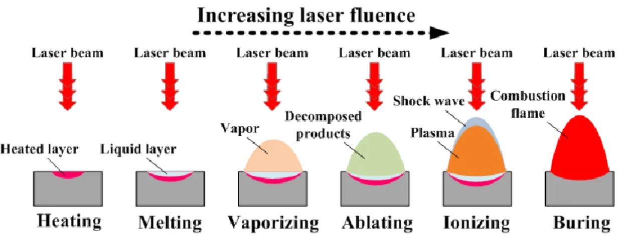
and 266 nm (4th harmonic) wavelengths; the fiber laser, with 1070 nm; and the excimer laser, with wavelengths from 157 nm to 351 nm (figure 1.1). Figure 1.2 to 1.3 show schematic
diagrams of the machined results for different laser pulse widths [1,2]. The pulse width for
Nd:YAG laser (λ: 1064 nm) is short than for the CO2 laser (λ: 10.6 μm), thus, the Nd:YAG
machined quality, including heat affected zones (HAZs), micro cracks, surface debris, and
shock waves, is much better than that produced by CO2 laser machining. Moreover, the cost
of Nd:YAG and CO2 laser sources are less than others of similar power output. Therefore,
manufacturers adopt the nanosecond pulsed Nd:YAG laser for the manufacture of indium tin
oxide (ITO) thin films for touch panels, surface texturing of silicon substrates for hydrophilic
surface applications, backside writing of glass substrates for hydrophobic surface applications,
and surface treatment of hard coatings for glass-molding applications. In this dissertation, a
pulsed Nd:YAG laser was used to investigate the mechanical, optoelectric, and surface
2
Figure 1.1 Common high-power laser sources for industry.
Figure 1.2 Long-pulse laser matter interaction [1].
3
1.1.1 Electrode forming of TCO thin films
In recent years, transparency conductive materials were extensively used in 3C market
products (i.e. computer, communication, and consumer electronics) to meet the rapid
development of the electro-optical and semiconductor industry. Common transparent
conductive oxide thin film materials, such as TiO2, SnO2, In2O3, and ZnO are used. The thin
films of ZnO composition doped with aluminum, gallium, and tin elements are named
aluminum zinc oxide (Al:ZnO), the gallium zinc oxide (Ga:ZnO), and the zinc tin oxide (ZTO)
[3] films, respectively. Particularly, among them, indium tin oxide (ITO) material is popularly
used in the flat panel display industry. Due to the high optical transparency and better
electrical conductivity, ITO films have attracted great interests for various electrode or
conductor applications in solar cells [4,5], flat panel displays [6], liquid crystal displays
(LCDs) [7], and in organic light emitting diodes [8]. Figure 1.4 shows the touch panel
applications including an Elonex e-Book reader and an Apple iPhone [9,10].
Figure 1.4 Products of touch panel application. (a) Elonex e-Book reader [9] and (b) Apple
iPhone [10].
In order to fulfill light, thin, short, small, and flexible requirements in the electronic
gadgets, plastic substrates are developed and convinced to be better candidates to replace the
glass substrate in portable electronic products. The most common used substrate materials
include polycarbonate (PC), polyestersulfone (PES), polyethylene terephtalate (PET),
4
polyimide (PI), polyarylate (PAR), and polyolefin. Figure 1.5 shows the schematic diagram of
fundamental structure for resistive touch panel [11]. In the electrode manufacturing process,
the transparent conductive material films were coated on these substrates first using the
various deposition methods, and then etching the deposited film to become the electrode of
the pre-determined pixel sizes.
Figure 1.5 Schematic diagram of fundamental structure for resistive touch panel [11].
Traditional electrode patterning techniques used the photolithography and chemical wet
etching to form the patterns on the thin deposited films. The film electrodes manufacturing
process includes sequentially (a) photoresist coating, (b) soft bake, (c) exposure, (d)
lithography, (e) hard bake, (f) etch, and (g) photoresist stripping [12]. Figure 1.6 shows the
semiconductor processes for patterning electrodes of transparent conductive oxide. Because of
these processes increasing the heavy investment of semiconductor lithography process
equipment and the chemical harm to the environment, a novel technique of direct laser writing
5
Figure 1.6 Semiconductor processes for patterning electrodes of transparent conductive oxide.
1.1.2 Wettability of material surfaces
Wettability is an important characteristic of solid surfaces. Due to continual
development in the field of nanotechnology in recent years, a deeper understanding of the
relationship between the microstructure of solid surfaces and wettability has been obtained.
Wettability can usually be shown through the contact angle between water and a solid surface.
Figure 1.7 shows the schematic diagram of a wettable surface [13]. When the contact angle is
smaller than 90°, the surface is referred to as a hydrophilic surface, and when the contact
angle is greater than 90°, it is referred to as a hydrophobic surface. A solid surface with a
6
Figure 1.7 Schematic diagram of a wettable surface [13]. (a) Superhydrophobic surface, (b)
hydrophobic surface, and (c) hydrophilic surface.
The wettability of a solid surface is decided by the chemical composition and
microscopic geometric structure. Under the effects of the solid surface chemical composition,
the higher than free energy of the solid surface, the higher the wettability is. The opposite is
also true. However, when adjusting the surface free energy using chemical methods, the
contact angle cannot usually be increased beyond 120°. In order to achieve a larger contact
angle, the surface material must be planned on a microscopic level. The microstructure of the
surface must be smaller than the micro-size of the liquid droplet. This micro structure can
effectively increase the hydrophilic or hydrophobic qualities of the material. Hydrophobic
materials are widely used to prevent pollution [14], prevent corrosion [15], reduce fluid
resistance [16-18] and also include self-cleaning mechanisms [19-21]. Hydrophilic materials
are widely used to disperse water evenly, dry faster, dissipate static electricity, and resist the
dirt and spots. Figure 1.8 shows a digital microfluidic biochip and a multifunctional
biochemical detection biochip system for the surface wettability application [22].
Figure 1.8 Products of surface wettability application [22]. (a) Digital microfluidic biochip
and (b) multifunctional biochemical detection biochip system.
7
1.1.3 Hard coatings for glass-molding dies
Glass materials have excellent optical properties, such as a high refractive index and low
optical energy absorption in visible light spectrum, and high chemical and heat resistance, and
are one of important materials used in the variety of key components and devices. Glass
materials are much more suitable than plastic materials applied for high temperature, humid
or harsh environments. For those reasons, glass lenses are dominantly used in optoelectronic,
chemical, and biomedical devices. Low cost and high performance glass lenses are mostly
produced by high precision molding technology. Figure 1.9 shows the photo-pictures of a
glass-molding machine and a glass-molding die [23]. Consequently, the protective films are
necessary for the glass molding dies to resist elevated temperature and pressure. The
protective films of different chemical compositions and processes are developed to satisfy the
different glasses operated conditions and to improve and extend the molding die lifetime.
In the glass-molding processes, several steps were needed, including (a) set glass
material onto molds, (b) vacuuming inside of the chamber, (c) purging exposure inside of the
chamber by nitrogen gas, (d) heat mold and glass materials to specified temperature by
infrared lamps, (e) vacuuming inside of the chamber, (f) clamping molds and pressing glass
materials, (g) cooling down molds and molded lenses with nitrogen gas, and (h) un-loading
molded lenses from molds after cooling to the specified temperature as shown in the Fig. 1.10
[24]. Figure 1.11 shows the application of glass-molding process for fabricating various lenses
such as bi-concave lens, bi-convex lens, meniscus lens, insertion lens, prism, f-θ lens, micro
8
Figure 1.9 Pictures of a glass-molding system [23]. (a) Glass-molding machine of
Toshiba-GMP207HV and (b) glass-molding die.
Figure 1.10 Flow diagram for glass-molding processes [24].
(a)
(b)
9
Figure 1.11 Application of glass-molding process for fabricating various lenses [24].
1.2 Motivation and objectives
The purposes of this dissertation are to develop surface processing technologies
including surface scribing, surface texturing, backside writing, and surface treatment of
materials and to better understand the interaction between laser beam and materials by the
nanosecond pulsed Nd:YAG laser processing system. The electrode isolation using laser
direct writing techniques on ITO films deposited on substrates is used in the various mobile
phones. The candidated substrates include soda-lime glass, polycarbonate (PC), and
cyclic-olefin-copolymer (COC). The operation parameters for the thin films material removal
in laser scribing are laser exposure time and scanning speed. The advantages of this method
are to reduce the heavy investment of semiconductor lithography process equipment and to
decrease the chemical harm to the environment compared with the wet etching process.
To reduce the production costs and increase the processing speeds, current laser micro-
or nano-machining processes employ techniques such as laser ablation, laser milling, and
laser deposition. These techniques have been effectively used to manufacture components
with enhanced wettability properties. A laser-ablated technique has been used to create rough
patterns on a silicon substrate to enhance the surface wettability. Moreover, a laser-induced
backside writing (LIBW) process and laser-induced plasma assisted ablation (LIPAA)
technique on a soda-lime glass substrate via ablation of metal target are to fabricate
10
characteristics, such as contacted angle, size and shape, can be measured by a surface tension
analyzer.
In the glass-molding or in the glass hot embossing process, a preform glass is heated 20
℃ to 40℃ above its yield point and pressed in a pumped nitrogen gas atmosphere. The working temperatures are approximately 500 ℃ for glasses such as P-SK57, N-PK51,
L-LAM69, which are usually used in most molding applications with a low transformation
temperature (Tg). However, the fused silica has a high Tg point, and must be heated to 1400℃
-1500 ℃ before pressed. This study aims to found an operation environment of the
glass-molding process by laser irradiations and to investigate the interaction between a laser
beam and protective coatings under an ambient atmosphere and a temperature of 1500℃. A
commercial finite element analysis (FEA) software was used to simulate the temperature
profile of these Ir-based alloy films irradiated by pulsed Nd:YAG laser because the
temperature generated by pulsed laser is difficult to monitor by practical measured methods.
The pulsed laser treatment technique has many advantages such as fast, energy-saving, and
novel excelling over other traditional furnace treatment. In addition, the properties such as
surface roughness, morphology, oxidation, microhardness, and reduced modulus are also
discussed. Finally, the simulation results and experimental results are compared.
1.3 Structure of the dissertation
The mechanical, optoelectric, and surface characteristics of materials processed by the
nanosecond pulsed Nd:YAG laser system are completely discussed in this dissertation. The
contents of each chapter are briefly described as follows:
Chapter 1 : Introduction. The backgrounds including (a) electrode forming of transparent
conductive oxide (TCO) deposited on various substrates for touch panels, (b)
wettability of material surfaces, and (c) hard coatings of glass-molding dies,
11
Chapter 2 : Literatures review. The literatures review of (a) laser scribing of TCO thin films,
(b) wetting effects of various textured surfaces, (c) protective coating
compositions for glass-molding dies, and (d) laser treatment technology of
material surfaces are introduced.
Chapter 3 : Laser processing mechanisms and parameters. Laser radiation absorption
mechanisms, laser direct writing techniques, laser-induced backside writing
techniques, and laser processing parameters are introduced and defined.
Chapter 4 :Experimental apparatus and sample preparation. In this dissertation, laser
processing experiments for various materials include (a) laser scribing of indium
tin oxide (ITO) thin films deposited on various substrates for touch panels, (b)
surface wettability of silicon substrates enhanced by laser ablation, (c)
hydrophobic templates with rough patterns fabricated by laser micromachining for
liquid droplets generation, and (d) characteristics of Ni-Ir and Pt-Ir hard coatings
surface treated by pulsed Nd:YAG laser irradiation. The Nd:YAG laser processing
setup, the laser processing parameter, the sample preparation, the numerical
simulation, the wettability characteristic, the measured method and instrument are
illustrated in this chapter.
Chapter 5 : Experimental results and discussion. After numerical simulation and laser
processing, all the experimental and simulation results of mechanical,
optoelectronic, and/or surface characteristics are measured and discussed.
Chapter 6 : Conclusions and future work. The conclusions of current studies and suggestions
12
Chapter 2 Literatures review
2.1 Laser scribing of TCO thin films
The conventional manufacturing method of the electrode forming was generally carried
out by photolithography and wet chemical etching. A complete-cycle process of the
conventional method required several processing steps consisting of photoresist (PR) coating,
soft bake, exposure, lithography, hard bake, chemical etching, and PR stripping. Moreover,
these high investment equipments and multi-steps increased the production cost and were
time-consuming. Simultaneously, the PR coating, acid etching, and PR stripping processes
also caused extra environmental pollution. Therefore, several issues to reduce fabricating cost
and environmental pollution were proposed recently. Among them, laser ablating techniques
were widely adopted in the microelectronic industries including (a) front-end and back-end
semiconductor fabrication processes, (b) advanced test and interconnects, (c) flat panel
display, (d) micromachining, and (e) others (i.e. solar cell, disk device, and nano-fabrication)
[25]. A novel approach, laser direct-writing method, was purposed to reduce the high
investment of semiconductor lithography processing equipment and to decrease the chemical
harm to the environment.
Some researches discussed the thin film ablation using different laser sources. Venkat
and Dunsky [6] proposed the laser pattering of indium tin oxide (ITO) films in panel display
manufacturing using different types of laser source: Nd :YVO4, Nd :YLF, and Nd :YAG.
Additionally, the direct write and mask based process were explained for micromachining
applications. Yoo et al. [26] proposed the different combination layers of Al, Ag, and Au
deposited on glass or plastic substrates. In the experimental procedure, the pulsed Nd :YAG
laser beam with 1064 nm wavelength, 10 Hz the pulse repetition frequency, 6 ns the pulse
width, and 8.5 W the maximum average power was performed to the sharp-edged patterns of
13 patterning different thin-film layers [26].
Figure 2.1 SEM images of Ag/Au pattern (a), Al/Ag pattern (b), edge-peeled Al/Ag stripe
pattern fabricated by two-beam interference (c), and micro-tubes formed by furtherincreasing
the pulse power (d) [26].
Chae et al. [27] presented a high resolution patterning of ITO thin films using an excimer
laser scanning projection process. Figure 2.2 shows the schematic illustration of
high-resolution ITO patterning process [27]. The amorphous ITO (a-ITO) films were
deposited on substrates by sputtering process at room temperature. These films then were
crystallized selectively after excimer laser crystallization projection. Finally, the ITO patterns
could be obtained by wet etch process for removal of the residual a-ITO films. Solieman [28]
conducted a spin coating method to deposit nanoparticulates on glass substrates. The
patterning was cured by a laser processing system, and the emitted light wavelengths could be
modulated ranging from 200 nm to 600 nm. Moreover, this system could adjust different feed
speeds of moving stages ranging from 0.01- 0.35 mm/s for controlling the energy density and
the film temperature. Shin et al. [29] fabricated high resolution patterning of ITO thin films
for electronic devices by using a pulsed Nd :YAG laser. The Nd :YAG laser patterning
technique was used to ablate the ITO films that could generate the circuit on the conductive
14 of patterned films [29].
Figure 2.2 Schematic illustration of high-resolution ITO patterning process [27].
Figure 2.3 Optical profiler images of patterned Au (top) and ITO (bottom) films (a) and ITO
patterns created using holographically patterned Al layers (b) [29].
Yavas and Takai [30,31] used the Q-switch Nd:YLF laser and flash lamp-pumped
15
absorption of ITO thin films and the observed morphology differences. Moreover, the
temperature model was used to confirm that ITO films were removed by the evaporative
mechanism. Lunney et al. [32] used the KrF excimer laser to ablate the fluorine-doped tin
oxide and indium tin oxide transparent conductive thin films. The 50 μm wide conducting
channel was ablated and measured by a scanning electron microscope. Molpeceres et al. [33]
used three types of laser source, including KrF excimer laser, Nd:YAG laser, and diode
pumped solid state (DPSS) laser, for patterning the amorphous silicon (a-Si) and ITO thin
films.
Park et al. [34] used an ultrafast laser with wavelength of 810 nm and pulse width of 150
fs to ablate the ITO thin film coated on the glass substrate. Both laser fluence and number of
pulses affect the ablation region depth. Figure 2.4 shows the ablation depths and widths at
different fluences measured by increasing the number of laser pulses [34]. With increasing the
number of pulses at the laser fluence well above the ablation threshold, the ablated depth
increases and then converges to a constant value of about 200 nm. The ablation threshold of
the ITO film conducted by the ultrafast laser was found to be 0.07 J/cm2 that is much lower than that of the glass substrate (about 1.2-1.6 J/cm2), which leads to a selective ablation of ITO films without damage on glass substrate.
Figure 2.4 Ablation depths and widths at different fluences measured by increasing the
16
Chen et al. [35] developed a third harmonic Nd:YAG laser system to direct writing
patterns on ITO films and discussed the effect of the different feeding speeds and pulse
repetition frequencies on the patterned line overlapping rate. Figure 2.5 shows the UV laser
direct writing of ITO thin films with different feed rates [35]. By increasing the laser scanning
speed and pulse repetition frequency, the patterned line width decreased.
17
Chen et al. [36] also used the laser beam shape technique to obtain top-hat intensity
distribution laser beam to perform line scribing and to perform electrode patterning on ITO
thin films deposited on glass and plastic substrates. Figure 2.6 shows the schematic diagram
of laser beam transmittance [36]. The obtained morphology of the complex patterning
electrode was uniform, smooth, and free from damage in substrates after the laser patterning
was performed. Qiao et al. [37] used a Nd:YAG laser with wavelength of 1064 nm and pulse
duration of 40 ns, and also used a Nd:YVO4 laser with wavelength of 355 nm, pulse duration
of 40 ns, and a Gaussian-to-top-hat convert to scribe in-house textured gallium-doped zinc
oxide (GZO) thin films coated on glass substrates for amorphous silicon photovoltaic (PV)
applications. The smooth edges and flat bottoms of the scribed lines were achieved by an
ultraviolet (UV) laser system.
18
Kim et al. [38] adopted a pulsed Nd:YAG laser with TEM00 mode and ablated the FTO
thin films coated on soda-lime glass substrates. The experimental results showed that a
pin-hole size of 1.6 mm diameter had the perfect TEM00 mode and the parameters of the best
ablation trace included the overlapping rate of 62%, the feeding speed of 6.08 mm/s, the pulse
repetition frequency of 10 Hz, and the charging voltage of 1000 V. Figure 2.7 shows the SEM
images of the surface morphology ablated by the Nd:YAG laser at different overlapping rates:
(a) 0%, (b) 25%, and (c) 62% [38]. Hass et al. [39] used pulsed lasers with wavelength of
1064 nm and 532 nm for patterning of ZnO/Ag back contact on the thin-film silicon modules.
For the microcrystalline silicon, a good patterning quality could be obtained by a green laser
or a NIR-laser with short pulse duration.
Figure 2.7 SEM images of the surface morphology of ablated by the Nd:YAG laser at
different overlapping rate: (a) 0%, (b) 25%, and (c) 62% [38].
2.2 Wetting effects of various textured surfaces
With improvements in material processing, orderly microstructure rough surfaces are
usually created by advanced surface processing techniques such as laser [40-43], dry-etching
or wet-etching [44], diamond dicing [18], and lithography [45]. In addition, the coating
technology is used to obtain superhydrophobic surfaces by creating nanostructures on the
19
machines by Yoshimitsu et al. [18] are orderly one-dimensional microgroove structures and
pillarlike microgroove structures. The surface is then coated with a layer of fluoroalkylsilane
(FAS), and water droplets are then used to compare the hydrophobicity and sliding behavior.
The results showed that the difference in surface feature and surface roughness will affect the
hydrophobicity and sliding angle of the surface. Figure 2.8 shows the pictures of 1 mg water
droplets on prepared pillar structures, corresponding different water contact angles, roughness
factors, and pillar heights machined by a dicing machine [18].
Figure 2.8 Pictures of 1 mg water droplets on prepared pillar structures [18].
Kannan and Sivakumar [40] utilized the diamond paste-polishing machine and laser
processing machine to individually manufacture stainless steel materials. They obtained a
0.013 μm smooth surface roughness and a single direction groove surface. They also studied
the impact process of water droplets on the hydrophobic surface as shown in Fig. 2.9 [40].
The geometry of the groove structure determines the liquid spreading after impacting the
surface. The liquid spreads along the direction of the groove. Due to the solid pillars of the
groove surface, the vertical spreading of the liquid in the groove is comparatively slower. Lee
et al. [46] utilized different surface roughness to design and manufacture a switchable
membrane device. This device attaches a thin polydimethylsiloxane (PDMS) membrane
20
than 2 μm. This membrane device can switch from moderate hydrophobicity to
superhydrophobicity by deflecting the membrane with a pneumatic method after testing.
Figure 2.9 Spreading-process images of water droplets with different impact conditions on the
hydrophobic grooved surface [40].
Chen et al. [47] adopted four types of hydrophobic materials including AZ6112, Teflon,
Parylene C, and plasma polymerization fluorocarbon film (PPFC) to fabricate the
hydrophobic textured surfaces with microstructures by using the standard lithography process.
21
were used to develop a droplet manipulating device as shown in Fig. 2.10 [47]. Because of
these templates without external power consumption and without side effect problems, the
proposed device can be applied in the droplet manipulation of microfluidic systems and in
thermal or electrical applications. Figure 2.11 shows the dynamic motion of a droplet on a
separated route [47].
Figure 2.10 SEM photos of the textured surfaces fabricated by using the standard lithography
process, (a) chain-configuration and (b) concentric circular configuration [47].
Figure 2.11 Dynamic motion of a droplet on a separated route [47].
(a)
22
Kim et al. [48] developed hexagonally arranged closed-packed concave nanotextures of
master surface of nanoporous alumina to imprint on aluminum films and gold films by
thermal evaporation and on polystyrene films by spin coating. The nanotextured templates
were used to calculate with measured water contact angles that decreased with depending
strongly on the materials and shapes of duplicating nanotextures. Figure 2.12 shows the
topology, the chemical reactivity, and the wettability of various nanopatterned aluminum films
[48].
Figure 2.12 FESEM images (top), EDX analysis spectra (middle), and water contact angles
(bottom) of various nanopatterned aluminum films [48].
Dahotre et al. [49] demonstrated a laser-based surface modification technology to
improve the wettability of the Ti-6Al-4V alloys to physiological fluids. The groove and pillar
23
contact angle. The roughness factors of these patterns were measured and plotted as a function
of laser fluence, as shown in Fig. 2.13(a) [49]. The measured results could be observed that
the roughness factor increased slightly with increasing laser fluence for both patterns.
Furthermore, the critical wetting angles of these patterns were measured and plotted as a
function of laser fluence, as shown in Fig. 2.13(b) [49]. The measured results could be
observed that the critical wetting angle increased with increasing laser fluence for both
patterns. The roughness factor of pillar patterns was higher than that of groove patterns;
therefore, the critical wetting angle of pillar patterns was larger than that of groove patterns.
Figure 2.13 Variation in roughness factor (a) and critical wetting angle with laser fluence for
groove and pillar patterns (b) [49].
Stojanovic et al. [50] demonstrated a developed coating composed of superhydrophobic
24
on machined templates. A near-ultraviolet Nd:YAG laser with a wavelength of 355 nm and a
pulse repetition frequency of 10 kHz were used to perform the nanofilament. Figure 2.14
shows the system of two immiscible liquids with suppressed evaporation and accurate
positioning of the aqueous liquid [50]. This approach can be used for open channel
microfluidics and microarray analysis due to its simplicity, the low cost, and the chemical and
environmental stability. Oliveira et al. [51] used a KrF laser to ablate polyimide surfaces that
had different microstructures as a function of the laser fluence ranging from 35 J/cm2 to 155 J/cm2. The surface morphology and static contact angle of these laser-ablated surfaces were measured and discussed. The measured results revealed that the apparent contact angle of the
laser-ablated surfaces increased with increasing the laser fluence. Moreover, the apparent
contact angle of the laser-ablated surfaces could reach values as high as 162° compared with
75° for the un-ablated polyimide surfaces.
Figure 2.14 System of two immiscible liquids with suppressed evaporation and accurate
positioning of the aqueous liquid: (a) schematic diagram of laser-ablated patterns and (b)
25
Luo et al. [52] used an excimer laser with a wavelength of 248 nm to etch the steel
surface to form different micro-patterns. The patterned surface became more hydrophobic
after depositing amorphous carbon (a-C) thin films using a magnetron sputtering technology.
The contact angle of a-C coating on laser patterned surface was approximately large than 10°
to 20° that of on the laser patterned surface. Bekesi et al. [53] used a short-pulse UV laser
combined with a fused silica-based diffractive optical element (DOE) to rapidly fabricate a
steel mold. This DOE was applied to distribute the laser energy into a 25 × 25 dot matrix and
as a transmission mask for laser ablation of steel mold. The laser-ablated mold was used to
replicate superhydrophobic surfaces on polypropylene by using variothermal injection
molding processes. The measured results showed that these contact angles of
superhydrophobic surfaces were more than 160°. Noh et al. [54] conducted a study of
hierarchically micro- and nano-structured mold surfaces using laser ablation for mass
production of superhydrophobic surfaces. The picoseconds laser source used in this
experiment was a Nd:YVO4 laser with a wavelength of 1064 nm, a pulse width of 12 ps, and
maximum pulse repetition frequency of 640 kHz. These microstructures on the mold surface
were replicated onto polydimethylsiloxane (PDMS) using a polymer casting method to
fabricate low-cost superhydrophobic surfaces. Figure 2.15 shows the micro- and
nano-structures of a nature lotus leaf and a laser-ablated mold [54]. The measured results
showed that the maximum contact angle of the water on the smooth PDMS surface and on the
replicated PDMS surface were 91°±1.5° and 157°±3°, respectively. Tang et al. [55] proposed
superhydrophobic surfaces fabricated by the femtosecond laser micromachining and chemical
vapor deposition to constitute micro- and nano-structures formed for carbon nanotube (CNT)
cluster. Plasma treatment was subsequently executed on growth of CNT clusters to enhance
the surface hydrophobicity. The wetting property of CNT surface with plasma treatment was
improved from hydrophilicity to superhydrophobicity, and the contact angle was 161°. This
26 vehicles, home windows, road lamps, and so on.
Figure 2.15 SEM images of a natural lotus leaf (a, b) and SEM images of laser-ablated micro-
and nano-structures and ripple formation (d, e) [54].
2.3 Protective coating compositions for glass-molding dies
Tungsten carbide (WC) was used as the mold material in glass-molding process. This
material is very hard and brittle but offers good performance in glass-molding dies. Pt-Ir, CrN,
CrWN, and Mo-Ru thin films are reported to coat mold surface and to increase the lifetime of
molds. Tseng et al. [56] discussed mechanical properties of Pt-Ir and Ni-Ir binary alloys for
glass-molding dies coating. Figure 2.16 is SEM pictures and shows a series of cross sectional
structures of the Ir-based deposits on the silicon wafer with Cr as buffer layer [56]. With
increasing Pt and Ni doping contents in Ir-based coatings, the microhardness of both coatings
decreased significantly and the values of reduced modulus of Pt-Ir alloys are larger than that
of Ni-Ir alloys. After the oxidation testing of these Ir-based coatings exposed at 700℃ by a
27
with increasing Pt contents. However, the oxygen concentration of Ni-Ir coatings shows large
variations even though the glass molding operation was conducted under the N2 atmosphere.
Figure 2.16 Cross-sectional micrographs of Cr, Pt-Ir and Ni-Ir coatings [56]. (a) Pt-Ir 1 (27.67
at.% Pt), (b) Pt-Ir 2 (55.25 at.% Pt), (c) Pt-Ir 3 (79.42 at.% Pt), (d) Ni-Ir 1 (26.10 at.% Ni), (e)
Ni-Ir 2 (51.44 at.% Ni), (f) Ni-Ir 3 (73.45 at.% Ni).
Lin et al. [57] proposed CrWN coatings with the tungsten contents of 0-23.4 at.%
coated on WC substrates by ion beam assisted deposition. Figure 2.17 shows the
(a) Pt-Ir 1 (b) Pt-Ir 2
(c) Pt-Ir 3 (d) Ni-Ir 1
(e) Ni-Ir 2 (f) Ni-Ir 3
Si substrate Cr layer
Pt-Ir layer Pt-Ir layer
Pt-Ir layer Ni-Ir layer
28
cross-sectional micrographs of chromium nitride based coatings [57]. With 4.4 at.%, 7.1 at.%,
13.1 at.%., and 19.7 at.% tungsten doping contents in CrN coatings, the smooth surfaces were
obtained and surface roughness Ra less than 2 nm. After oxidation test at 750℃ in air
atmosphere, the Cr2O3 precipitates were formed and resulted in the large roughness of more
than 40 nm on the CrN and CrWN coatings surface. However, the CrWN coatings with 4.4
at.% to 16.7 at.% tungsten contents revealed smooth surface and improved hardness that can
be applied in glass-molding die coatings.
Figure 2.17 Cross-sectional micrographs of chromium nitride based coatings [57]. (a) CrN
and (b) CrWN4 (16.7 at.% W).
The Mo-Ru binary alloys with Cr and Ti twin buffer layers deposited on WC substrates
as the protective coatings was investigated [58,59]. Figure 2.18 shows the cross-sectional
TEM images of (a) Mo56.7Ru43.3/Cr/Ti(O)/WC deposit and (b) detailed structure of the
oxide scale, the transition zone and the columnar grains [59]. With the higher Ru doping
contents in Mo-based coatings, the results show that the Mo-Ru alloys have better oxidation
resistance but also have a higher surface roughness. Moreover, Wei and Shieh [60] proposed
the TaN binary compounds and Ta1-xWxNy ternary compounds deposited on the WC dies and
silicon wafers by ion beam sputtering. The Ta1-xWxNy films reveal better high temperature
29
high hardness, and chemical resistance. These films are anti-adhesive and have excellent
chemical stability and good coating stability under working environment. Moreover, laser
surface treatment can improve the toughness and durability of film materials to further
enhance the performance of the mold surface.
Figure 2.18 Cross-sectional TEM images of (a) Mo56.7Ru43.3/Cr/Ti(O)/WC deposit and (b)
detailed structure of the oxide scale, the transition zone, and the columnar grains [59].
2.4 Laser treatment technology of material surfaces
In 1941, Rosenthal [61] proposed a mathematic model to thermally evaluate the transient
temperature field of working pieces for point, line, and surface heating laser sources. Kang et
al. [62] applied a finite element program ABAQUS to analyze the heat transfer and residual
distortion for laser welding LD (laser diode) pump on EDFA (erbium doped fiber amplifier).
Figure 2.19 shows the temperature distributions at welding procedure of laser diode pump on
erbium doped fiber amplifier [62]. In the Nd:YAG laser welding process, distortion occurs at
the ferrule and saddle during the heating and cooling processes of welding. Gordon et al. [63]
provided a simulation tool for a laser manufacturing process. He discussed the relationship
between the pulse energy, the etch rate, the pulse frequency and the preheating temperature of
30
advantages of no contact between the tools and work specimens, high temperature, lack of
tool wear, high speed, and few thermal effects [64].
Figure 2.19 Temperature distributions at welding procedure of laser diode pump on erbium
doped fiber amplifier [62].
Liu et al. [65] discussed a pulse laser-textured method that uses a Co-based WC-TiC
sintered carbide coating. They also investigated the resulting microstructure, roughness,
hardness, and wear resistant properties of coatings. Figure 2.20 shows the cross-sectional
views of the alloyed layer textured with different laser power [65]. These measured results
reveal that the micrographs have three distinct regions including the laser melting zone (LMZ),
the heat affected zone (HAZ), and the non-affected zone (NAZ) existed in the interface
between the substrate and the coating. Textured surfaces have many advantages and the most
important one is to improve mechanical performance, such as surface hardness [66],
tribological behaviour [67], and lubricating of friction [68,69]. Wan [70] proposed a novel
laser coating and texturing technique to improve surface topographies and friction behaviour.
Tseng [43] reported a surface-texturing technique to create rough patterns on a silicon
31
Figure 2.20 Cross-sectional views of the alloyed layer textured with different laser power: (a)
![Figure 1.5 Schematic diagram of fundamental structure for resistive touch panel [11].](https://thumb-ap.123doks.com/thumbv2/9libinfo/8409034.179734/21.892.177.763.345.629/figure-schematic-diagram-fundamental-structure-resistive-touch-panel.webp)
![Figure 2.4 Ablation depths and widths at different fluences measured by increasing the number of laser pulses [34]](https://thumb-ap.123doks.com/thumbv2/9libinfo/8409034.179734/32.892.140.806.836.1077/figure-ablation-depths-widths-different-fluences-measured-increasing.webp)
![Figure 2.7 SEM images of the surface morphology of ablated by the Nd:YAG laser at different overlapping rate: (a) 0%, (b) 25%, and (c) 62% [38]](https://thumb-ap.123doks.com/thumbv2/9libinfo/8409034.179734/35.892.161.779.559.783/figure-images-surface-morphology-ablated-laser-different-overlapping.webp)
![Figure 2.8 Pictures of 1 mg water droplets on prepared pillar structures [18].](https://thumb-ap.123doks.com/thumbv2/9libinfo/8409034.179734/36.892.166.772.425.679/figure-pictures-mg-water-droplets-prepared-pillar-structures.webp)
![Figure 2.9 Spreading-process images of water droplets with different impact conditions on the hydrophobic grooved surface [40]](https://thumb-ap.123doks.com/thumbv2/9libinfo/8409034.179734/37.892.153.785.223.837/figure-spreading-process-droplets-different-conditions-hydrophobic-grooved.webp)
![Figure 2.16 Cross-sectional micrographs of Cr, Pt-Ir and Ni-Ir coatings [56]. (a) Pt-Ir 1 (27.67 at.% Pt), (b) Pt-Ir 2 (55.25 at.% Pt), (c) Pt-Ir 3 (79.42 at.% Pt), (d) Ni-Ir 1 (26.10 at.% Ni), (e)](https://thumb-ap.123doks.com/thumbv2/9libinfo/8409034.179734/44.892.207.729.224.867/figure-cross-sectional-micrographs-coatings-ir-pt-ni.webp)
![Figure 2.20 Cross-sectional views of the alloyed layer textured with different laser power: (a) P = 500 W, (b) P = 700 W, (c) P = 900 W [65]](https://thumb-ap.123doks.com/thumbv2/9libinfo/8409034.179734/48.892.310.625.107.737/figure-cross-sectional-alloyed-textured-different-laser-power.webp)