國 立 交 通 大 學
電信工程學系
碩 士 論 文
Ku 頻修正型 24 路功率分配器及應用於
Wi-Fi 和 WiMAX 寬頻共平面波導平衡至非平
衡轉換
Ku-band Modified 24-way Power Divider
and
Broadband Co-planar Waveguide Balun for
Wi-Fi and WiMAX Applications
研究生:王惟婷
指導教授:張志揚 博士
Ku 頻段修正型功率分配器及應用於 Wi-Fi 和
WiMAX 寬頻共平面波導平衡至非平衡轉換
Ku-band Modified 24-way Power Divider and
Broadband Co-planar Waveguide Balun for Wi-Fi
and WiMAX Applications
研 究 生:王惟婷 Student:Wei-Ting Wang
指導教授:張志揚 Advisor:Chi-Yang Chang
國 立 交 通 大 學
電信工程學系
碩 士 論 文
A Thesis
Submitted to Department of Communication Engineering
College of Electrical and Computer Engineering
National Chiao Tung University
in partial Fulfillment of the Requirements
for the Degree of Master of Science
in
Communication Engineering
June 2007
Hsinchu, Taiwan, Republic of China
Ku 頻段修正型功率分配器及應用於 Wi-Fi 和
WiMAX 寬頻共平面波導平衡至非平衡轉換
研究生:王惟婷 指導教授:張志揚 博士
國立交通大學電信工程學系
摘要
數位傳播的衛星電視訊號操作於 Ku 頻(12GHZ~14GHZ),在車用衛
星電視系統中,需要一個 24 路的功率分配器將訊號傳送至由 24 個偶
極天線組成的陣列天線。然而,功率分配器在 Ku 頻段有互耦及接合
點效應的問題。本文嘗試改變 Wilkinson 功率分配器,將
λ/2 傳輸線
加入
λ/4 傳輸線中及隔離電阻和輸出端,以改善上述的問題。
現今有相當多的無線技術,為了涵蓋更多的無線規格需要寬頻的
元件。文中以共平面波導的方式實做一個適用 Wi-Fi 和 WiMAX 頻段寬
頻的 Marchand 平衡至非平衡轉換。頻寬取決於阻抗的比值,共平面
波導結構可以輕易的實現高阻抗和低阻抗,達到寬頻的效果。
Ku-band Modified 24-way Power Divider and
Broadband Co-planar Waveguide Balun for Wi-Fi
and WiMAX Applications
Student: Wei-Ting Wang Advisor: Chi-Yang Chang
Department of Communication Engineering
National Chiao Tung University
Abstract
Digital broadcast satellite transmits signal in the Ku frequency range (12
GHz to 14 GHz ). To feed the array antenna composed of 24 dipoles, we
need a 24-way power divider. However, power divider in Ku band suffers
junction effects and mutual coupling. We modified the equal-split
Wilkinson power divider by adding λ/2 transmission lines to λ/4 branches
and isolation resistor to output ports to overcome those problems.
There are a lot of wireless technologies in the world. To include more
wireless standards, broadband devices are required. The broadband balun
has the potential to provide various wide-band applications that are
included Wi-Fi and WiMAX. We will develop a broadband Marchand
balun using Co-planar waveguide (CPW) structure. Bandwidth depends
on impedance ratio, and it is easy to realize high and low impedance in
CPW by spacing the gaps and shunting more transmission lines.
誌謝
首先,感謝指導教授張志揚博士,學問上老師博大精深的微波學
識讓我獲益良多,體力上老師爬山和騎單車的功力更是讓我敬佩。
感謝實驗室的學長和同仁,老是讓我問問題但是都不會煩的均
翔,及常一起討論的雄哥、哲慶,合成濾波器強者小谷,很忙的惠諄
學長,還有健談的建育,謝謝你們一路上給予我的幫助。同窗的梁八、
英公、為崧、慶鴻、銘哥,實驗室生活因為有了大家而很精彩充滿朝
氣。謝謝梁蓉幫我校稿,若有人稱讚我的論文、投影片排版很好,她
是幕後功臣。
最後要謝謝我的家人,在我求學路上的一路付出,讓我無後顧之
憂地求學和生活。
Table of Contents
List of Figures ...vii
List of Tables...x
Chapter 1 Introduction...1
1.1 Satellite Television...1
1.2 Wi-Fi and WiMAX ...3
Chapter 2 Modified 24-way Power Divider ...6
2.1 Equal-split Wilkinson Power Divider ...6
2.2 3-Way Hybrid Power Divider ...16
2.3 24-way Power Divider ...31
Chapter 3 Broadband Planar Marchand Balun...33
3.1 Analysis of the Marchand Balun...34
3.2 Realization of the Marchand Balun ...40
Chapter 4 Conclusion ...56
List of Figures
Figure 1-1: Satellite dish...2
Figure 1-2: Satellites are higher in the sky than TV antennas, so they have a much larger "line of sight" range. ...2
Figure 1-3: Different wireless technologies in the world. ...5
Figure 2-1: The Wilkinson power divider circuit in normalized and symmetric form. ...7
Figure 2-2: Bisection of the circuit of Figure 2-1 (a) Even-mode excitation (b) Odd- mode excitation...8
Figure 2-3: The standard equal-split (3 dB) Wilkinson power divider. ...9
Figure 2-4: The 3 4 λ Wilkinson power divider with high translational degree for the exact placement of the chip resistor...10
Figure 2-5: Two semi-circle branches with electrical length of 90˚ at 12.45 GHz..11
Figure 2-6: The simulation result of Figure 2-5...12
Figure 2-7: The measured data of the circuit of Figure 2-5...12
Figure 2-8: The new geometry with 3 4 λ branch and 2 λ transformer...14
Figure 2-9: The realized circuit of the modified Wilkinson power divider. ...15
Figure 2-10: The simulation result of Figure 2-9...15
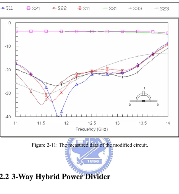
Figure 2-11: The measured data of the modified circuit...16
Figure 2-12: The Wilkinson n-way hybrid power divider...17
Figure 2-13: (a) Radial-type n-way hybrid power divider (b) The inner arrangement of n wires and resistors. ...17
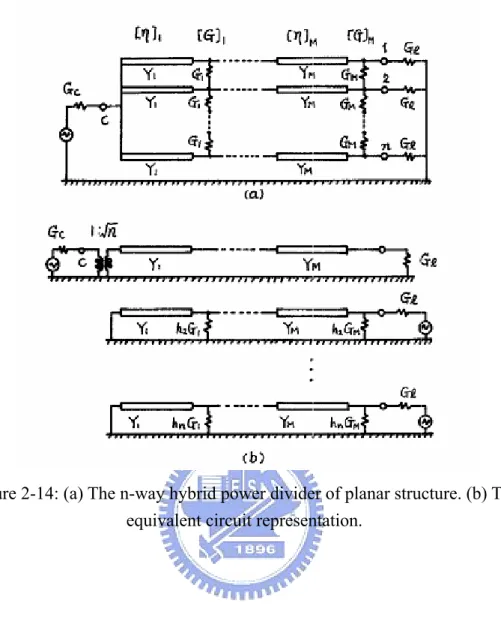
Figure 2-14: (a) The n-way hybrid power divider of planar structure. (b) The equivalent circuit representation...18
Figure 2-15: (a) A three-way planar hybrid power divider. (b)The equivalent circuit. ...21
Figure 2-16: (a) The equivalent even mode circuit (b)(c) The equivalent odd mode circuits...24
Figure 2-17: The relation between the isolation resistor and s parameter of one stage. ...25
Figure 2-17: 3-way power divider with Z1= 3Z0 =86.8Ω, R=100Ω. ...25
Figure 2-19: The measured data of the circuit in Figure 2-15. ...26
Figure 2-20: The measured isolation of 3-way power divider...27
Figure 2-21: 24-way power divider...27
Figure 2-22: The measured isolation of port1 and port3 in Figure 2-21. ...28
Figure 2-23: The measured response of the 24-way power divider...28
Figure 2-24: 8-way power divider...29
Figure 2-25: The triangle is the measured path of the leftist path of the 3 splits in Figure 2-21. The square is the measured phase difference of the bended middle path and the leftist straight path...30
Figure 3-1: Marchand balun coaxial cross section. ...36
Figure 3-2: Equivalent transmission line model. ...36
Figure 3-3: (a) A four-port coupled line and (b) its equivalent circuit...37
Figure 3-4: Basic logic of the Marchand balun [5]...37
Figure 3-5: Coupled-line Marchand balun and its equivalent circuit. ...38
Figure 3-6: Marchand balun equivalent circuit parameters as a function of load impedance (a)3:1 bandwidth, (b)5:1 bandwidth [6][8]...39
Figure 3-7: Marchand balun coupled-line parameters as a function of load impedance for (a) 3:1 bandwidth (b) 5:1 bandwidth...40
Figure 3-8: Couple-line model...42
Figure 3-9: The response of couple-line model. ...42
Figure 3-10: The first layout of couple-line balun...43
Figure 3-11: The simulation result of the 1st layout of couple-line balun...43
Figure 3-12: The measured data of the 1st layout of couple-line balun. ...44
Figure 3-13: The measured phase imbalance (top) and the amplitude imbalance (bottom) of the first type couple-line balun. ...44
Figure 3-14: The second layout of couple-line balun. ...46
Figure 3-15: The simulation result of the 2nd layout of couple-line balun...46
Figure 3-16: The measured magnitude response of the 2nd layout of couple-line balun. ...47
Figure 3-17: The measured phase imbalance (top) and the amplitude imbalance (bottom) of the 2nd layout of couple-line balun. ...47
Figure 3-18: The Marchand balun model. ...49
Figure 3-19: The response of Marchand balun. ...50
Figure 3-20: The first layout of Marchand balun...50
Figure 3-21: The simulation result of the 1st layout of Marchand balun. ...51
Figure 3-22: The measured magnitude response of the 1st layout of Marchand balun. ...51 Figure 3-23: The measured phase imbalance (top) and the amplitude imbalance
(bottom) of the 1st layout of Marchand balun ...52 Figure 3-24: The 2nd layout of Marchand balun. ...52 Figure 3-25: The simulation result of the 2nd layout of Marchand balun. ...53 Figure 3-26: The measured magnitude response of the 2nd layout of Marchand balun.
...53 Figure 3-27: The measured phase imbalance (top) and the amplitude imbalance
(bottom) of the 2nd Marchand balun...54 Figure 3-28: The realized baluns *cm. ...54 Figure 3-29: The realized baluns *cm. ...55
List of Tables
Table 1-1: IEEE 802.11x Wireless Communication Standard. ...5
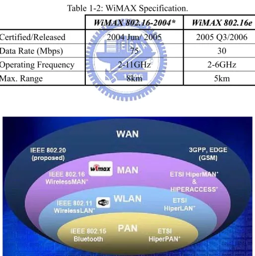
Table 1-2: WiMAX Specification. ...5
Table 2-1: The responses of half of the 24-way power divider...29
Chapter 1
Introduction
1.1 Satellite Television
Satellite television technology had been successfully broadcasted in 1974 in the United State. However, it did not hit the market; because, home dishes were expensive metal units that took up a huge chunk of yard space. In these early years, satellite TV was a lot more difficult than broadcast and cable TV. Today, you see compact satellite dishes perched on rooftops. The major satellite television companies are bringing in more customers every day with the lure of movies, sporting events and news from around the world.
Satellite television is a lot like broadcast television. It's a wireless system for delivering television programming directly to a viewer's house. Both broadcast television and satellite stations transmit programming via a radio signal. But satellite solves the problems of range and distortion by transmitting broadcast signals from satellite orbiting the Earth. Since satellites are high in the sky, there are a lot more customers in the line of site, so the received range will be large than broadcast TV. Satellite television systems transmit and receive radio signals using specialized
antennas called satellite dishes as shown in Figure 1-1. Early satellite television was broadcast in C-band radio -- radio in the 3.4 GHz to 7 GHz frequency range. Digital broadcast satellite transmits programming in the Ku frequency range (12 GHz to 14 GHz).
Figure 1-1: Satellite dish.
Figure 1-2: Satellites are higher in the sky than TV antennas, so they have a much larger "line of sight" range.
In our program, we want to set satellite TV whose frequency range is Ku band (12.2GHz~12.7GHz) in car, but the satellite dishes are not adaptive to the car environment for its solidity. We make a microstrip array antenna to replace the dishes, because of planarity and small dimension. We set the array antenna on the roof of the car and under the metal cover. The array antenna is composed of 24 dipole antennas. To feed the array antenna, we need a 24-way power divider.
In Chapter 2, the 24-way power divider is composed of a 3-way power divider and 3 8-way power dividers. Each 8-way power divider consists of 7 equal split (3db) power dividers. Power divider in Ku band will suffer junction effects and mutual coupling. To overcome these problems, we add a
2
λ
transmission line in two places; one is between the output port and the isolation resistor, and the other is the
4
λ
transmission line branch. The 4
λ
branches will become 3 4
λ
long.
1.2 Wi-Fi and WiMAX
IEEE 802.11 also known by the brand Wi-Fi, denotes a set of Wireless LAN (WLAN)
standards. It was developed by working group 11 of the IEEE LAN Standards Committee (IEEE 802). 802.11b and 802.11g standards use the 2.4 GHz band. Because of choosing this frequency band, 802.11b and 802.11g equipment will suffer interference from microwave ovens, cordless telephones, Bluetooth devices and other
appliances using this same band. The 802.11a standard uses a different 5 GHz band, which is clean by comparison. 802.11a devices are not affected by products operating on the 2.4 GHz band. 802.11n is a new multi-streaming modulation technique that has recently been developed. 802.11n builds upon previous 802.11 standards by adding MIMO (multiple-input multiple-output). MIMO uses multiple transmitter and receiver antennas to allow for increased data throughput via spatial multiplexing and increased range by exploiting the spatial diversity. Antennae are listed in a format of 2x2 for two receivers and two transmitters.
WiMAX is defined as Worldwide Interoperability for Microwave Access by the
WiMAX Forum, formed in June 2001 to promote conformance and interoperability of the IEEE 802.16 standard, officially known as WirelessMAN. WiMAX aims to provide wireless data over long distances, in a variety of different ways, from point to point links to full mobile cellular type access.
Figure 1-3 shows different wireless technologies in the world. Each standard’s frequency rang has some difference. However, people hope their products could all in one at the most time. No matter Wi-Fi, WiMAX or Bluetooth, we could use them all. So, the broadband devices rise. And, the broadband balun has the potential to provide various wide-band applications that are included Bluetooth, Wi-Fi and WiMAX. In Chapter 3, we will develop a broadband Marchand balun using Co-planar waveguide
(CPW) structure.
Table 1-1: IEEE 802.11x Wireless Communication Standard.
Table 1-2: WiMAX Specification.
W WiiMMAAXX880022..1166--22000044** WWiiMMAAXX880022..1166ee Certified/Released 2004 Jun/ 2005 2005 Q3/2006 Data Rate (Mbps) 75 30 Operating Frequency 2-11GHz 2-6GHz Max. Range 8km 5km
Chapter 2
Modified 24-way Power Divider
Multi-port microstrip power dividers, used in array antenna, usually use the Wilkinson designs. The standard Wilkinson design has problems at higher frequencies due to coupling and junction effects between the output branches. In this chapter we utilize modified 2-way power divider to overcome those problems.
2.1 Equal-split Wilkinson Power Divider
2.1.1 Even-Odd Mode Analysis
We excite two modes for the equal-split Wilkinson power divider circuit of Figure 2-1
[1]:the even mode,
V
g2=V
g3=V
0, and the odd mode,V
g2=−
V
g3=V
0. Superpositionof these two modes, we have an excitation of
V
g2=2V
0,V
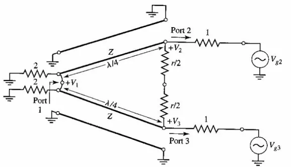
g3=0, we can have the SFigure 2-1: The Wilkinson power divider circuit in normalized and symmetric form.
Even mode. For the even mode excitation,
V
g2=V
g3=V
0, and so 2eV
= 3eV
, the middle of the symmetric circuit is a magnetic wall (PMC), so there is no current flow through the2r resistors and the point between the inputs of the two transmission lines at port1. Thus we can bisect the network of Figure 2-1 by the mid plane to obtain the network of Figure 2-2(a). Then, looking into port2, we see an impedance
e in Z = 2 2 Z (2.1)
Since the transmission line looks like a quarter-wave transformer, thus, if Z = 2, prot2 will be matched for even mode excitation; then 2e
V
=1 02
V
sincee in
Z =1. The
2r resistor is superfluous in this case, since one end is open-circuited.
Odd mode. For odd-mode excitation,
V
g2=−
V
g3=V
0, and so 2oV
= 3oV
a electric wall (PEC) along the middle of the circuit in Figure 2-1. Thus, we can bisect this circuit by grounding its mid-plane to get the network like Figure 2-2(b). Looking into port2, we see an impedance of
2
r , since the transmission line is
4
λ
long and shorted at port1, and it looks like an open circuit at port2. So, port2 will be matched for odd mode excitation if we select r = 2 .For this mode of excitation all power is delivered to the
2r resistors, none going to port1.
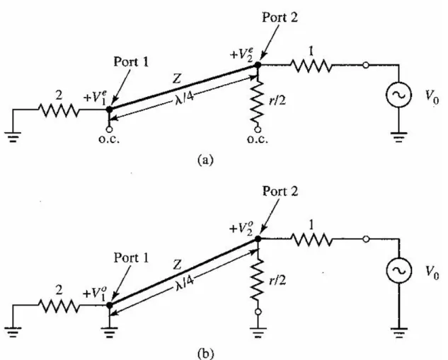
Figure 2-2: Bisection of the circuit of Figure 2-1 (a) Even-mode excitation (b) Odd- mode excitation.
So, the standard equal-split (3 dB) Wilkinson power divider in Figure 2-3 comprises two branches that have an impedance of 2Zo and an electrical length of
90°
at the center frequency of the divider. The lumped resistor R, which isconnected between the outputs of the two branches, provides the required isolation.
Figure 2-3: The standard equal-split (3 dB) Wilkinson power divider.
Usually Wilkinson power divider is used at X-band frequencies or below. When frequencies above X-band several problems arise. If the chip resistor has a resonance frequency comparable to the operating frequency, it will no longer behave like a lumped element. Then, to achieve a high chip-resistor resonance frequency, the chip dimensions must be very small, about the order of 40 x 20 mil. This means that the two branches of the power divider must be placed very close to connect to the resistor. This gives rise to strong mutual coupling and junction effects between the output lines.
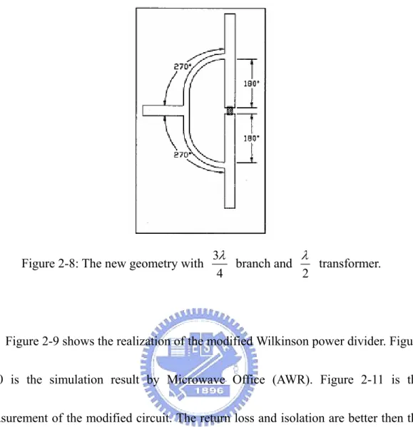
And, at the higher frequencies, it is difficult to bend the branches into a semi-circle. The most common solution to this problem is to use branch length of 3
4
λ
, rather than
4
λ
[2]. However, there is a high translational degree of freedom for the exact placement of the chip-resistor between the two branched of the divider. These problems are illustrated in Figure 2-4.
Figure 2-4: The 3 4
λ
Wilkinson power divider with high translational degree for the exact placement of the chip resistor.
Due to the proximity of the output of the two branches, there is coupling between them. This decreases the isolation between the output ports, and because of the sharp corner between the branch and output line we will expense the input return loss.
Figure 2-5 shows the realized circuit is fabricated using Rogers 4003( 3.38
r
and the two branches have the electrical length of
90°
at 12.45 GHz.Figure 2-6 is the simulation by circuit simulator Microwave office (AWR). Figure 2-7 shows the measured data from the circuit of Figure 2-5. The input return loss of the measured response at 12.45GHz is -15.61 dB, the output return loss is -25.23 dB, the isolation is -17.24 dB, and insertion loss is -3.5 dB.Figure 2-6: The simulation result of Figure 2-5.
2.1.2 The Modified Wilkinson Power Divider
The modification to the Wilkinson design solves the problems mentioned above, but has the expense of the bandwidth of the device and the larger circuit size. However, our specification is the center frequency of 12.45GHz and the bandwidth is from 12.2 GHz to12.7GHz. It is narrow band about 4%, so we can endure the expense of bandwidth, and in this project, we don’t care about the size.
This is achieved by opening the circle formed by the two branched into a semi-circle and connecting the resistor to the ends of the branches via
2
λ
lengths of 50Ω transmission line.
The new geometry is shown in Figure 2-8 [2]. The 2
λ
lengths of 50Ω transmission line transform the impedance of the chip-resistor to the output branches at the designed frequency, but the impedance is not correct at the frequencies away from that. Thus, it reduces the operating bandwidth. However, the output coupling and sharp corner problems are resolved.
Figure 2-8: The new geometry with 3 4 λ branch and 2 λ transformer.
Figure 2-9shows the realization of the modified Wilkinson power divider.Figure 2-10 is the simulation result by Microwave Office (AWR). Figure 2-11 is the measurement of the modified circuit. The return loss and isolation are better then the original one.
Figure 2-9: The realized circuit of the modified Wilkinson power divider.
Figure 2-11: The measured data of the modified circuit.
2.2 3-Way Hybrid Power Divider
2.2.1 N-Way Hybrid
There are 3 types of n-way hybrids, 1) the Wilkinson, 2) the radial, 3) the fork n-way hybrids [3]. The Wilkinson n-way hybrid shown in Figure 2-12 satisfies the required properties of match and isolation, electrical symmetry, and low loss. The low-loss results from that the signal travels only a quarter wave length independent of the value of n. The problem for Wilkinson hybrid is its nonplanarity for n > 2, as shown in Figure 2-12. The reason for the nonplanarity of the Wilkinson n-way hybrid is the
topology of its isolation resistors.
The radial hybrid shown in Figure 2-13 needs n/2 (n even) or (n-1)/2 (n odd) sections of n-wire lines and coaxial-type isolation resistors for matching at the center frequency. However, it still is a nonplanar structure. The folk hybrid, on the other hand, produces a completely planar geometry shown in Figure 2-14.
Figure 2-12: The Wilkinson n-way hybrid power divider.
Figure 2-13: (a) Radial-type n-way hybrid power divider (b) The inner arrangement of n wires and resistors.
Figure 2-14: (a) The n-way hybrid power divider of planar structure. (b) The equivalent circuit representation.
2.2.2 The n-Way Planar Hybrid Power Divider
We get isolation resistors of a planar structure by connecting n-1 resistors at the ends of the neighboring wires of the n-wire lines. The n-way planar hybrid power divider is shown in Figure 2-14. It is designed by using M sections of n uncoupled
4
λ
transmission lines with the planar isolation resistors. We can analysis the circuit by getting the eigenvalues and the eigenvectors of the characteristic admittance matrix for the n transmission lines and the admittance matrix for the n-1 isolation resistors.
The planar n-way hybrid has M sections of n 4
λ
transmission lines and M sections of n-1 isolation resistors, so there are M characteristic admittance matrices and M admittance matrices for n-1 isolation resistors. The n-1 isolation resistors compose an n-ports network, and we can derive its admittance matrix. In this circuit, we define the n x n real symmetric matrix [H] as follows [3]:
[H] =
1
1 0
0
1 2
1
0
0
1 2
1
0
0
1 1
⎡ ⎤ ⎢ ⎥ ⎢ ⎥ ⎢ ⎥ ⎢ ⎥ ⎢ ⎥ ⎢ ⎥ ⎢ ⎥ ⎣ ⎦−
−
−
−
−
−
"
%
#
% % %
#
%
"
(2.2) The eigenvaluseh
i
( i = 1,2,….,n) of matrix [H] are obtained as2 2cos ( 1) /
h
i
n
i
= −
π
−
( i = 1, 2,……,n) (2.3)The eigenvector corresponding to the eigenvalue
h
1= 0 is ⎡⎣1 1
"
1 t
⎤⎦ . The eigenvectors corresponding to the eigenvaluesi
h
( i = 2,……,n) arewhere
( 1) /
i
n
i
φ
=
π
−
.By normalizing these eigenvectors, we get a real orthogonal matrix[ ]
PH .The admittance matrices
[ ]
G μ of the planar isolation resistors can be representedaccording to matrix [H] as
[ ]
G μ =Gμ[ ]
H (μ=1,…,M) (2.5) Therefore,[ ] [ ] [ ]
t 0, 2, ..., H H n P G μ P =diag⎡⎣ G hμ G hμ ⎤⎦ (2.6)The characteristic admittance matrices
[ ]
η μ of the n transmission lines are presented[ ]
η μ =Yμ1n (μ=1,…,M) (2.7)where 1n represents the n x n identity matrix. Therefore,
[ ] [ ] [ ]
t 1H H n
P η μ P =Yμ (μ=1,…,M) (2.8)
Since all the admittance matrices of the planar isolation resistors and all the characteristic admittance matrices of the transmission lines are transformed into diagonal matrices according to the orthogonal matrix
[ ]
PH , the (1,n)-port shown inFigure 2-14 (a) can be equivalently transformed into a two-port of the even-mode circuit and n-1 one-ports of the odd-mode circuits as shown in Figure 2-14 (b). The two port circuit is represented by a quarter-wave transformer of M sections. The characteristic admittances Y1, , M"Y are decided by the maximally flat transformer or
the chebyscheff transformer.
For n-1 one port circuits are satisfied the following n-1 equations
2 2 1 1 2 3 3 2 2 1 M l l M M i M i i i Y G h G Y h G Y h G Y h h G − − = + + + + # i=(2,…..,n) (2.9)
,then each one-port matches at the center frequency where electrical length of the line section θ equals π/2. Since Y1, , M"Y have been selected, if M=n-1, then G1, ,"GM can
be selected.
2.2.3 Three–Way Planar Hybrid Power Divider
A three-way planar hybrid circuit can be obtained by using 2 section of 3 transmission lines and planar isolation resistors as shown in Figure 2-15(a). The
[ ]
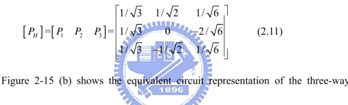
H matrix is[ ]
11 21 01 0 1 1 − ⎡ ⎤ ⎢ ⎥ = −⎢ − ⎥ ⎢ ⎥ ⎣ ⎦ H (2.10)The eigenvalues of [H] are h1=0,h2 =1,h3 =3, and the orthogonal matrix
[ ]
PH is[ ]
PH =[
P1 P2 P3]
= 1/ 3 1/ 2 1/ 6 1/ 3 0 2 / 6 1/ 3 1/ 2 1/ 6 ⎡ ⎤ ⎢ ⎥ − ⎢ ⎥ ⎢ ⎥ − ⎢ ⎥ ⎣ ⎦ (2.11)Figure 2-15 (b) shows the equivalent circuit representation of the three-way planar power divider. All the impedances of the input and three output ports be 50Ω, the two-port circuit is represented by a quarter-wave transformer of 2 sections with a transformation ratio 150Ω:50Ω.If we consider the maximally flat transformer, the characteristic impedances Z1 =114 ,Ω Z2 =65.8Ω . In order that the two one-port
circuits match at the center frequency, the planar isolation resistors are
1 65 , 2 200
2.2.4 One Stage 3-way Power Divider
The equivalent circuits of the one stage 3-way power divider are shown in Figure 2-16.
Figure 2-16 (a) is the even mode circuit, and Figure 2-16 (b), (c) are the odd mode circuits. In Figure 2-16 (a),
2 2 2 1 1 1 2 2 2 1 1 3 3 3 3 3 3 o in o L o o o L o in Y Y Y Y Y Y Y r Y Y Y Y Y Y Y − − − = = = + + + (2.12) If we choose 1 3 o Y
Y = , than r1 = Γ = . It is perfect match at the input port. 0, 1 0
From Figure 2-16 (b), (c), we can get
1 2 2 1 2 1 2 1 2 1 2 1 2 1 2 1 2 1 1 1 1 o o L L o o G Y G Y Y G g G Y G Y G g Y λ λ λ λ λ λ λ λ − − − − Γ = = = = + + + + (2.13) 1 3 3 1 3 1 3 1 3 1 3 1 3 1 3 1 3 1 1 1 1 L o o L o o G Y G Y G Y g G Y G Y G g Y λ λ λ λ λ λ λ λ − − − − Γ = = = = + + + + (2.14)
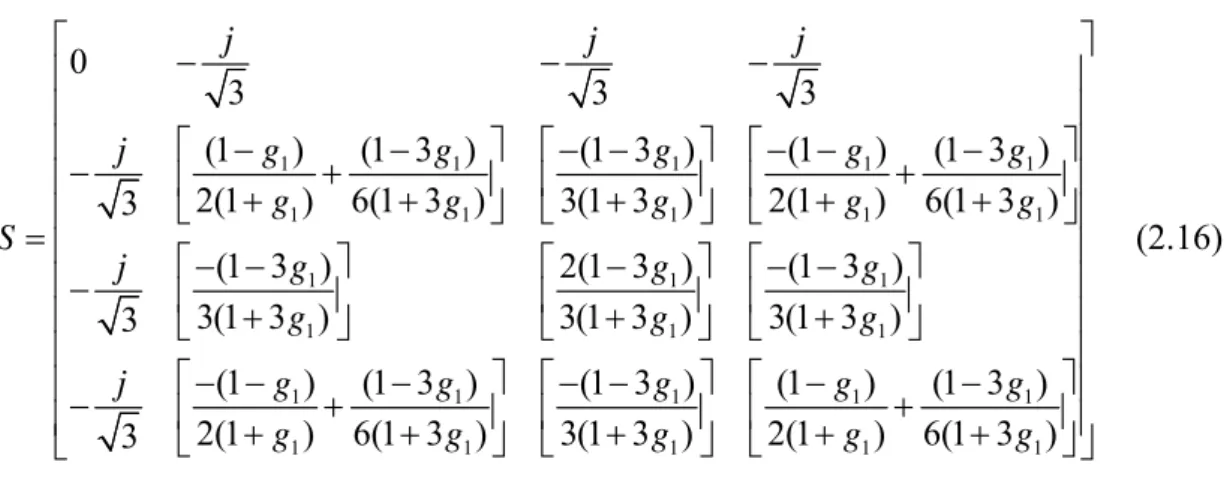
We could derive the s parameters of the power divider by the following equation
[4]: ' ' 1 , , , , 2 N i j j i m i m j m m S S q q N = Γ = = +
∑
Γ i,j=1,2,…,N (2.15) 1Γ the output return loss of the even mode circuit. ( 2,3..., )
m m N
Γ = the return losses of the odd mode circuits.
,
m i
q factor of the ith row of the mth normalized eigenvector
1 1 1 1 1 1 1 1 1 1 1 1 1 1 1 1 1 1 0 3 3 3 (1 ) (1 3 ) (1 3 ) (1 ) (1 3 ) 2(1 ) 6(1 3 ) 3(1 3 ) 2(1 ) 6(1 3 ) 3 (1 3 ) 2(1 3 ) (1 3 ) 3(1 3 ) 3(1 3 ) 3(1 3 ) 3 (1 ) (1 3 2(1 ) 3 j j j g g g g g j g g g g g S g g g j g g g g g j g − − − ⎡ − − ⎤ ⎡− − ⎤ ⎡− − − ⎤ − ⎢ + ⎥ ⎢ ⎥ ⎢ + ⎥ + + + + + ⎣ ⎦ ⎣ ⎦ ⎣ ⎦ = ⎡− − ⎤ ⎡ − ⎤ ⎡− − ⎤ − ⎢ ⎥ ⎢ ⎥ ⎢ ⎥ + + + ⎣ ⎦ ⎣ ⎦ ⎣ ⎦ − − − − + + 11 11 11 11 ) (1 3 ) (1 ) (1 3 ) 6(1 3 ) 3(1 3 ) 2(1 ) 6(1 3 ) g g g g g g g ⎡ ⎤ ⎢ ⎥ ⎢ ⎥ ⎢ ⎥ ⎢ ⎥ ⎢ ⎥ ⎢ ⎥ ⎢ ⎥ ⎢ ⎥ ⎢ ⎥ ⎡ ⎤ ⎡− − ⎤ ⎡ − − ⎤ ⎢ + ⎥ ⎢ ⎥ ⎢ ⎥ ⎢ ⎥ ⎢ ⎣ + ⎦ ⎣ + ⎦ ⎣ + + ⎦⎥ ⎣ ⎦ (2.16)
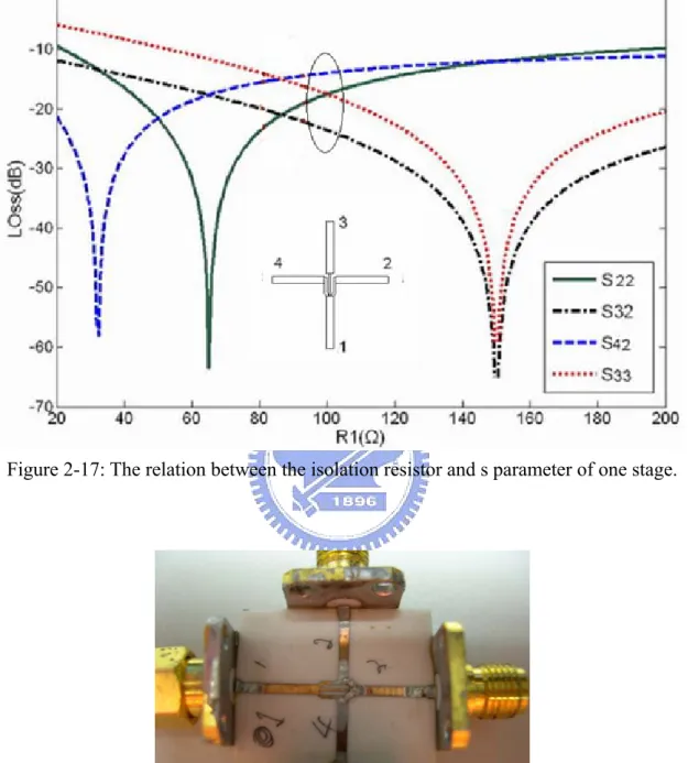
Figure 2-17shows the relation between the isolation resistor and the s parameters of the power divider.
We choose Z1= 3Zo =86.8 ,Ω R=100Ω for our circuit shown in Figure 2-18.
Since it is not easy to get chip resistor which size is 40 mil x 20 mil, we choose the isolation resistor we have already had in our Lab.
0
3
Y
Y1 YL=Y0 1Γ
Y1 YL=Y0 2G
1λ
Γ
2 Y1 YL=Y0 3Γ
3G
1λ
r
1 Yin (a) (b) (c)circuits
Figure 2-17: The relation between the isolation resistor and s parameter of one stage.
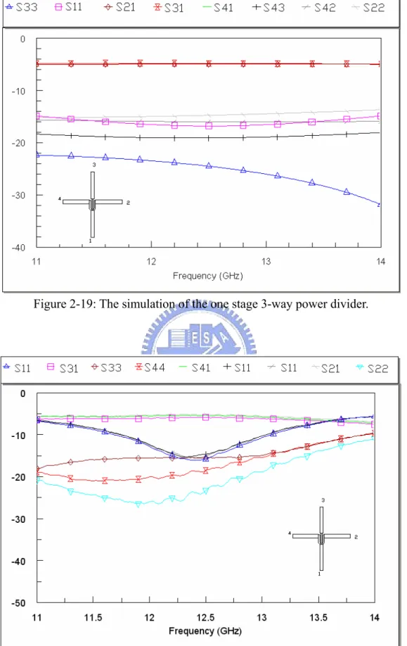
Figure 2-19: The simulation of the one stage 3-way power divider.
Figure 2-21: The measured isolation of 3-way power divider.
Figure 2-23: The measured isolation of port1 and port3 in Figure 2-22.
Table 2-1: The responses of half of the 24-way power divider. S11 S21 S22 phase port0→port1 -16.19 dB -20.24 dB -19.14 dB -23.87 ゚ port0→port2 -15.28 dB -20.13 dB -19.84 dB -26 ゚ port0→port3 -15.01 dB -20.65 dB -13.2 dB -50.19 ゚ port0→port4 -15.6 dB -20.37 dB -13.6 dB -53.69 ゚ port0→port5 -15.47dB -20.94 dB -12.25 dB -62.39 ゚ port0→port6 -16.5 dB -20.2 dB -13.6 dB -69.72 ゚ port0→port7 -15.82 dB -19.86 dB -18.53 dB -69.88 ゚ port0→port8 -15.03 dB -20.21 dB -15.02 dB -75.89 ゚ port0→port9 -16.17 dB -20.9 dB -15.24 dB -85.88 ゚ port0→port10 -14.91 dB -21.51 dB -9.47 dB -97.62 ゚ port0→port11 -16.29 dB -21.06 dB -12.12 dB -90.38 ゚ port0→port12 -16.13 dB -21.77 dB -13.2 dB -88.59 ゚
Table 2-2: The response of 8-way power divider. port 1 2 3 4 5 6 7 8 phase -113.47゚ -129.14゚ -119.65゚ -119.05゚ -125.17゚ -127 ゚ -126.57゚ -126.33゚ Δphase 15.4 ゚ 0 ゚* 9.55 ゚ 9.96 ゚ 4 ゚ 2.2゚ 2.68 ゚ 2.77 ゚ IL(db) -10.94 -11.28 -11.13 -11.39 -11.49 -11.3 -11.56 -11.13 * reference
Figure 2-26: The triangle is the measured path of the leftist path of the 3 splits in Figure 2-22. The square is the measured phase difference of the bended middle path
The one stage 3-way power divider has been simulated by Microwave Office (AWR). Figure 2-19 shows the simulated results, Figure 2-20 and Figure 2-21 is the measured data. The input return loss is about -15dB at 12.45 GHz. The insertion losses of the three separated paths are -5.5dB. The isolation between port2 and port4 is -13.46dB, and port2 and port3 is -17.3dB at 12.45GHz. We choose the isolation resistor, R=100Ω, we have had, because chip resistor is not easy to get for the size about 40 x 20 mil.
2.3 24-way Power Divider
Figure 2-23 and Figure 2-24 are one of the measured responses of 24-way power divider. Because the response of each path is much similar, we just show one of them. It is the path, port0 to port1, the input return loss is -16.19 dB, the output return loss is -19.14 dB, and the insertion loss is -20.24 dB. Because the 24-way power divider is a symmetric circuit, we just have half of the measurements (port1 to port 12), as shown in
Table 2-1, and Figure2-22 shows the isolation between port1 and port3. The input return losses are better than -15 dB, and insertion loss of each path are pretty identified. However, the phase of each path is not very corresponded to each other. We think that there are two reasons. One is the bend of the cable of the network analyzer, because the 24-way power divider circuit is very big, we bended the cable into sharp curve when measuring. The smaller the circuit the smoother the cable curve, the phase measurement has less affection. The other is the 24-way circuit is too big (57.62cm x 12.41cm), but the board is so thin (20 mil=0.05cm), that the side of the board will drop down, and the phase measurements have affection. The farther the distance between port0 to the output port, the more the effect to the phase. If we have supports under the board, the phase difference will be improved. Table 2-2 and Figure 2-26 can support above description. While the circuit is smaller, the board is more planar and the phase of each path is corresponded highly. Table 2-2 is the measured response of 8-way power divider shown in Figure 2-24.
Chapter 3
Broadband Planar Marchand Balun
The word balun is an acronym for balanced-to-unbalanced converter, and the function is to change an unbalanced signal to a balanced signal with equal potential but opposite polarity. Baluns are key components in balanced circuit such as balanced-mixers, push-pull amplifiers, frequency doublers, antenna feed networks and phase shifters. Although, multi-octave active baluns have been reported, they not only consume dc power, but suffer from high noise figure, high spurious response, low power handling capability, and low 3rd order intermodulation intercept point. Therefore, a broadband passive balun is a dispensable element in realizing high performance microwave circuits.
Marchand balun is perhaps one of the most attractive due to its planar structure and wide-band performance [6]. Proper selection of balun parameters can achieve a bandwidth of more than 10:1. In Figure 3-2, the ratio of the characteristic impedances of short-circuited and open-circuited stubs determines the bandwidth; the higher the ratio, the wider the bandwidth. CPW (co-planar waveguide) can easily derive high impedance for widening the gap, and low impedance for shunting transmission lines.
Thus,CPW Marchand balun is a good way to derive broadband and planar balun.
3.1 Analysis of the Marchand Balun
The balun basically consists of an unbalanced, an open-circuited, two short-circuited, and balanced transmission line sections. Each section is about a quarter-wavelength long at the center frequency of operation. A coaxial version of a Marchand balun is shown in Figure 3-1, and its equivalent circuit representation is shown in Figure 3-2.
Synthesis of coaxial Marchand baluns is a available in the literature [6][7][8]. A Marchand balun can be realized using a pair of coupled lines as shown in Figure 3-3(a)
[6][8]. By properly selecting its parameters, we can design a planar balun to meet the
desired response. An equivalent of a coupled-line of equal conductor width is shown in Figure 3-3(b)where Z1 and Z2 are the characteristic impedances of distributed unit element, and N is the transformation ratio.
0c 0e 0o Z = Z Z (3.1) 0 0 0 0 e o e o Z Z k Z Z − = + (3.2) 0 0 1 1 e c k Z Z k + = − (3.3) 0 0 1 1 o c k Z Z k − = + (3.4) 0 1 2 1 c Z Z k = − (3.5)
2 2 0 2 1 o k Z Z k − = (3.6) 1 N k = (3.7)
The balun in Figure 3-5(a) has four elements and is known as fourth-order Marchand balun. Matching section Z makes it a fourth-order balun with improved broadband performance. Figure 3-5(b) and Figure 3-5(c) show equivalent circuit representations and Figure 3-5(d) shows further simplification when
a b
N =N = . N
Balun equivalent circuit parameters as a function of return loss for fourth-order Chebyshev filters having 3:1 and 5:1 bandwidth are given in Figure 3-6 [6][8] for a source impedance of 50Ω. Coupled-line parameters are plotted in Figure3-7. According to these curves in Figure 3-6and Figure 3-7, we can derive the parameters of Marchand balun. ' 2 2 1 2 1 a ac Z Z Z k N = = − (3.8) ' 2 2 2 2 1 b bc Z Z Z k N = = − (3.9) 2 ' 1 1 3 2 ( ) 2 1 a b ac bc Z Z k Z Z Z N k + = = + − (3.10) ' 2 4 2 Z Z Zk N = = (3.11) ' 2 5 2 R R Rk N = = (3.12)
Figure 3-1: Marchand balun coaxial cross section. Z2 Z0 Z1 ZS1 ZS1 a b ZB ZL
Figure 3-3: (a) A four-port coupled line and (b) its equivalent circuit.
Z R ka, Za kb, Zb (a) Z2a Z1a 1:Na Z Na:1 1:Nb Z1b R Z2b Nb:1 (b) Z2a Z1a 1:Na Z Na:1 1:Nb Z1b R Z2b (c) Z2b N2 Z2' Z2a N2 Z1' Z N2 Z4' R N2 R5' Z1a+Z1b N2 Z3' (d)
Figure 3-6: Marchand balun equivalent circuit parameters as a function of load impedance (a)3:1 bandwidth, (b)5:1 bandwidth [6][8].
Figure 3-7: Marchand balun coupled-line parameters as a function of load impedance for (a) 3:1 bandwidth (b) 5:1 bandwidth.
3.2 Realization of the Marchand Balun
The Marchand balun was fabricated using ceramic Al2O3 (εr=9.8) with CPW structure. The substrate thickness is 15 mils. We use 2 circuit models for the realization. Figure 3-8 is the couple-line model; it consists of 2 couple-line sections
and one 4
λ
transmission line, the transmission line transfers the impedance and enhances the bandwidth. Each electrical length of the transformer and couple-line is
4
λ
at center frequency. Figure 3-9 shows the response of couple-line balun. We design two layouts to implement this couple-line balun. The first layout, the ground plane appears only at one side of each couple-line, and we fold the two couple-lines to right and left side, as shown in Figure 3-10. The input port is at the bottom of the circuit, and the two output ports are on the upper right and upper left of the circuit. The couple-lines are with Lange type of layout with four fingers for the first and six fingers for the second couple-line. Because the odd mode impedance of the second couple-line is too low to use 4-lined couple-line, we use six-finger couple-line instead. Figure 3-11 is the simulated results where an EM simulator Sonnet is used, Figure 3-12 is the measured response, and Figure 3-13 shows the phase imbalance and amplitude imbalance of the measured responses. The S11 is less than -10dB in the range of 1.852 GHz to 6.429 GHz, and the fractional bandwidth is about 110%.
Figure 3-8: Couple-line model.
Figure 3-10: The first layout of couple-line balun.
Figure 3-12: The measured data of the 1st layout of couple-line balun.
Figure 3-13: The measured phase imbalance (top) and the amplitude imbalance (bottom) of the 1st layout of couple-line balun.
The second layout of the couple-line balun is shown in Figure 3-14. In this layout, the couplers are still with four and six fingers respectively. However, this layout has ground plans at both sides of each coupler. Because this layout does not fold, it is
4
λ
longer than the folded layout. However the bandwidth of the non-folded structure is much better than the folded one. Figure 3-15 shows the simulated responses by EM simulator Sonnet, Figure 3-16 depicts the measured response and Figure 3-17 shows the phase imbalance and amplitude imbalance of the measured responses. The upper frequency of the input return loss better than -10dB is 7.375 GHz, but the frequency of phase balance better than 10o is just 6.73 GHz, so the fractional bandwidth (Δf) is 130.7% not 140%.
Figure 3-14: The second layout of couple-line balun.
Figure 3-16: The measured magnitude response of the 2nd layout of couple-line balun.
Figure 3-17: The measurement of the phase unbalance (top) and the amplitude unbalance (bottom) of the 2nd layout of couple-line balun.
Figure 3-18 is the Marchand balun model. It consists of an unbalanced transmission line section, an open-circuited series stub, and two series connected short-circuited shunt stubs, each transmission line is
4
λ
at center frequency. Figure 3-19 is the response of the Marchand balun. We use different line width and gap to implement the characteristics z1, z2, zs1, zs2 in Figure 3-18. Figure 3-20 is the first layout of Marchand balun, in this layout, the minimal width of line is 2.1 mil. Figure 3-21 is the simulated result of the first layout of Marchand balun by EM simulator, HFSS, Figure 3-22 depicts the measured magnitude response, and Figure 3-23shows the phase imbalance and amplitude imbalance of the measured responses. The S11 is less than -10dB in the range of 1.519 GHz to 6.887 GHz, and the fractional bandwidth of the type1 circuit is 127.8%.
We can see Figure 3-24 is the second layout of Marchand balun, the minimal width of line is 3.3 mil. Figure 3-25 shows the simulated result of the second layout by HFSS. Figure 3-26 depicts the measured magnitude responses, and Figure 3-27 shows the measured phase imbalance and amplitude imbalance of the balun. The response of S11 is very good, and it is less than -20 dB in the most of the frequency range. The amplitude imbalance is within 0.65dB, and phase imbalance is less than 2 ゚ over the frequency range of 1.121 GHz to 5.477 GHz. The fractional bandwidth of this circuit is 132%. In Figure 3-18, the two series connected short-circuited shunt
stubs, zs1,zs2 equivalent to one short-circuited shunt stub with zs = 128Ω. So, it is the 3 orders Marchand balun but in Figure 3-26 the return loss seems like 4 orders. Beside this point, CPW realization Marchand balun is a good way to implement a broadband planar balun. Figure 3-28 and Figure 3-29are the realized CPW baluns.
Figure 3-19: The response of Marchand balun.
Figure 3-21: The simulation result of the 1st layout Marchand balun.
Figure 3-23: The measured phase imbalance (top) and the amplitude imbalance (bottom) of the 1st layout of Marchand balun
Figure 3-25: The simulation result of the 2nd layout of Marchand balun.
Figure 3-27:The measured phase imbalance (top) and the amplitude imbalance (bottom) of the 2nd layout of Marchand balun.
Chapter 4
Conclusion
In Chpter2, the measured results of the modified equal split Wilkinson power divider is improved compared with the 2-way Wilkinson power divider. The return loss of the 3-way one section power divider is about -15 dB , it is good for a microwave circuit. The insertion losses of the three outputs are balanced about -5.5 dB. The isolations between the neighborhood of the output ports are better than the isolation between the output ports, port2 and port4.
The 24-way power divider is a very symmetric geometry but each phase of the 24-way power divider is not identified. We think the cable of the network analyzer and substrate are the important factors. The sharp curve of the cable of network analyzer and the substrate’s flexibility influence the phase results.
In Chapter 3, we show two kinds of layouts for couple-line balun. One is folded structure, the two output ports go out at the top of it. And other is non-folded, the output ports are located at the middle of the balun. The results show the response of the non-folded structure is better than the folded. The possible reason is the couple-line in the non-folded balun is more close to the defined Co-planar waveguide
(CPW) couple-line structure. In the non-folded balun, the couple-line sees the ground plane at both sides, but in the folded one, it dose not.
In the later part of Chapter 3, we use different line width to implement Marchand balun. In our circuit model, there are 3 orders at most. However, the last circuit seems like 4 orders. Beside the point, the bandwidth and balance of amplitude and phase are good.
Compared with couple-line and Marchand baluns, we evaluate the performances of bandwidth, amplitude balance, phase balance and circuit size, the Marchand balun is a good choice for a broadband balun.
Reference
[1] David Pozar, Microwave Engineering, 3rd edition, John Wily & Sons, N.Y. 2005. [2] Dimitrios Antsos, Rick Crist and Lin Sukamto, “A Novel Wilkinson Power
Divider with Predictable Performance at K and Ka-band”, 1994 IEEE MTT-S Digest.
[3] Nobuo Nagai, Eiji Maekawa and Koujiro Ono, “New n-Way Hybrid Power Dividers”, IEEE Transactions on Microwave Theory and Techniques, Vol. MTT-25, No. 12, Dec 1977.
[4] 張秀琴,”W-band Switch and Ka-band Power Divider” 交通大學電信研究所, 2005
[5] 紀 鈞 翔 , “ LTCC Broadband Mixer and LTCC Filters for Wireless LAN Applications”, 交通大學電信研究所, 2004
[6] Rajesh Mongia, Inder Bahl and Prakash Bhartia, “RF and Microwave Coupled-Line Circuits”, 1999 Artech House.
[7] Cloete, J.H., “Exact Design of the Marchand Balun”, Microwaves J., Vol. 23, May 1980, pp. 99-110.
[8] Goldsmith, C. L., A. Kikel, and N. L. Wilkens, “ Synthesis of Marchand Baluns Using Multilayer Microstrip Strucures”, Int. J. of Microwave and Millimeter-Wave Computer-Aided Engineering, Vol. 2, July 1992, pp.179-188.
![TraditionalMLCalgorithmsmainlytacklethebatchMLCproblem,wheretheinputdataarepresentedinabatch[24,28].Nevertheless,inmanyMLCapplicationssuchase-mailcategorization[22],multi-labelexamplesarriveasastream.Onlineanalysisistherefore dimensionreducermotivatedbyma](data:image/gif;base64,R0lGODlhAQABAIAAAP///wAAACH5BAEAAAAALAAAAAABAAEAAAICRAEAOw==)