金屬奈米粒子表面電漿效應之研究
135
0
0
全文
(2)
(3)
(4)
(5) 中文摘要 本論文係以金屬奈米粒子表面電漿效應為研究主題,利用金屬奈 米粒子中之群體電子對入射電磁波的共振特性,進一步研究奈米粒子 的光學性質與潛在應用。本研究工作共分為三部分: 第一部分,銀奈米粒子即時吸收光譜之量測。利用即時吸收光譜 之量測技術,研究銀奈米薄膜在加溫過程中之動態光學行為。配合暗 視野光學顯微鏡、掃描式電子顯微鏡與原子力顯微鏡之觀察,確定金 屬粒子粒徑由 5 奈米成長至 250 奈米。在加溫過程中,並發現吸收光 譜具有藍移與紅移等現象。根據此即時且非破壞性之量測技術,可應 用於金屬奈米粒子光學特性及動態行為之分析。 第二部分,利用雷射脈衝製作有序金奈米粒子光柵結構。將兩道 -9. 同極化之 10 秒雷射短脈衝光入射在金奈米薄膜表面的相同區域,脈 衝的空間週期的光強度分布,使金奈米薄膜進行瞬間高溫退火處理。 結果顯示,受高溫退火的薄膜區域,形成金奈米顆粒;未受高溫退火 的區域則維持薄膜結構,故造成有序金奈米粒子分布之光柵。我們並 且發現金奈米粒子表面電漿效應對光柵第一階繞射效率產生貢獻,使 繞射效率為一波長函數之曲線。 第三部分,參雜銀奈米粒子之膽固醇液晶光柵繞射效率之研究。 由於金屬奈米粒子表面電漿共振波長可由週遭環境介電特性決定,故. I.
(6) 利用膽固醇液晶光柵來調製銀奈米粒子表面電漿效應。此銀奈米粒子 之週期性環境激發週期性表面電漿效應,並產生一額外繞射波段位於 表面電漿共振波長周圍。此研究成功應用膽固醇液晶作為調製表面電 漿共振的介質,並使表面電漿成為可藉由電壓控制之光學特性。 本研究主要實驗結果證實金屬奈米粒子的尺寸、尺寸分布、密度 及週遭環境介電特性,皆會影響金屬奈米粒子表面電漿效應。換言 之,表面電漿共振波長會隨金屬奈米粒子的尺寸或遭環境折射率變 化,此一特性以廣泛應用於生物感測或奈米光學元件。本文中,以 Mie 散射理論為基礎,討論金屬奈米粒子的吸收光譜特性,並分析群 體電子在電磁波影響下的運動,如何影響金屬奈米粒子之光學行為。. II.
(7) Abstract Collective oscillation of conduction electrons in metallic nanoparticles known as localized surface plasmon resonance has been studied for nano-optics applications. The excitation of localized surface plasmons on nano-structured metal material leads to strong light scattering and absorption. Since the localized surface plasmon resonance is strongly dependent on the shape, size, size distribution, and dielectric property of surrounding environment of nano-structured metal, the dependence can be applied in wide applications. However, the direct and non-destructed observation of nano-structured metal is required to the development of nano-technology, we proposed a real time optical observation due to the optical respons of metal nano-particles system. Furthermore, we proposed a fast and simple method to fabricate a high order metal nano-particles array and used liquid crystal material to directly modulate the surface plasmon effect on the metal nanoparticles. The purpose of this work is to study the surface plasmon effect excited on metal nanoparticles. These works are described as follows: A.. The topic of the first work is “Real time absorbance spectra due to optical dynamics of silver nano-particles film”, we report the real time absorbance spectra due to optical dynamics of silver nano-particles film under a heating treatment from 28 to 300 ℃. A 7nm-thicked sliver film was thermally deposited on an indium tin oxide glass substrate. In the process of heating, the real time absorbance spectra of silver nano-particles film were measured by an optical spectrometer. It was noted that the absorbance spectra of the film varied with the heat-treating temperature and time. The peak position in the spectra curve shifted to shorter wavelength below the temperature of 250 ℃, then shifted to red band due to higher temperature treatment. With the comparison of scanning electron micrograph analysis, the real time absorbance\ spectra exhibited a particular optical property confirmed by the dynamic dark-field optical microscopy system. The real-time absorbance spectra and dark-field micrographs analyses lead to a direct and non-destructed observation of growing evolution of metal nano-particles.. B.. The topic of the second work is “Laser pulse induced gold nanoparticles grating”. We report the results of our experimental investigation of laser induced gold nano-particle gratings and their optical diffraction properties. A single shot of a pair of Nd-YAG laser pulses of the same polarization is directed toward a thin III.
(8) gold film of thickness 6 nm on a substrate of polymethyl methacrylate (PMMA). As a result of the laser illumination, the thin gold film is fragmented into an array of nano-particles. Using scanning electron and dark-field optical micrographs, we discovered that the morphology of the gold nanoparticles grating is dependent on the fluence of laser pulse. The spectrum of first order diffraction shows a spectral dependence, possibly due to the presence of the nano-particles of various sizes. The ablation of thin films of nano-thickness via the use of laser pulses may provide a simple and efficient method for the fabrication of nano-scale structures, including 2D arrays of nano-particles. C.. The topic of the second work is “Surface plamons induced extra diffraction band of cholesteric liquid crystal grating”. We investigated the diffraction behavior of cholesteric liquid crystal (CLC) grating with the surface plasmon effect was investigated. One indium-tin-oxide plate of the CLC grating cell was covered with silver nanoparticles. With the application of a proper voltage, a well formed phase grating was constructed in the CLC cell. The CLC grating was probed by a beam of the polarized-monochromatic light, and the wavelength range was from 450 to 700 nm. It was shown that an extra first-order diffraction band was observed around 505 nm. The physical reason of the extra diffraction band could be the surface plasma effect emerged from silver nanoparticles. The extra diffraction band due to the surface plasmon effect can offer potential applications in nano-optics, such as the optical switch function.. IV.
(9) Acknowledgement First and foremost, my sincerest acknowledgement and gratitude go to Prof. Wood-Hi Cheng of my advisor and Prof. Ming-shan Tsai of my co-advisor. Their guidance and support throughout my graduate study and research lead me to overcome difficulty in the study. With their help and encouragement, I could achieve this study. I really feel very lucky to meeting both of you in this great time. I really thank Prof. I-Min Jiang and Prof. Pochi Yeh. They teach me how to figure out the solution of problem, how to organize the paper writing, and to build a correct attribute for good study. Thank your help in my study life. Without their help, I can’t be better in this work. You are the men bringing me lucky to everything. Thank you very very much. I also really thank my committee members, Prof. Andy Y. G. Fuh, Prof. Chia-Chen Hsu, Prof. Sheng-Lung Huang Prof. Tsong-Sheng Lay and Prof. Tsung-Hsien Lin, for serving my dissertation committee. Your comments complete this study. Thanks are extended to our group members and to all nice collaborators of my study period. Except my family, all you are always my best friends in my life. With your help, I could be happy in my study life. Finally, I really appreciate my parent and my brother and sister. I am the youngest in my family. All of you always take good care of me. I sincerely appreciate your support when I am in hard time. I am so honored being a member of this family. I have to tell you I will love you through my whole life. Dear grandfather, you should always take good care of me. I can feel that. I wish you being happy and healthy in the sky. I want to tell you that I got PhD degree already. You make me grow. I do love you. If I keep going to write some words to you, I will cry heavily. This thesis is for you.. V.
(10) Contents Abstract.. ........................................................................................................................ I Acknowledgements.......................................................................................................V List of Contents............................................................................................................VI List of Figures ..............................................................................................................VI List of Tables ...............................................................................................................VI Chapter 1 Introduction ...................................................................................................1 1.1 Background ............................................................................................................1 1.2 Motivation ..............................................................................................................3 1.3 Organization ...........................................................................................................3 Chapter 2 Study and application of metallic nano-particles system ............................7 2.1 Fundamental optical property of metal nanoparticles ............................................7 2.1.1. Geometry effect on localized surface plasmons ........................................7. 2.1.2. Dielectric effect on localized surface plasmons.........................................9. 2.1.3. Localized surface plasmons of metal nanorods .......................................10. 2.2 Preparation and Arraying of metal material .........................................................13 2.2.1. Photoinduced conversion of silver naonspheres to nanoprisms ..............13. 2.2.2. Electron beam lithography (nano-array)..................................................15. 2.2.3. Focused ion beam (FIB)...........................................................................16. 2.3 Application and development of localized surface plasmon resonance (LSPR) .19 2.3.1. Surface Plasmon Enhanced Raman Scattering ........................................19. 2.3.2. Interference of locally excited surface plasmons.....................................20. 2.3.3. Plasmon wave between metal nano-particle ............................................22. 2.3.4. Nanodot coupler with a surface plasmon polariton condenser ................26. 2.3.5. Surface-Plasmon-Coupled Emission of Quantum Dots...........................30. VI.
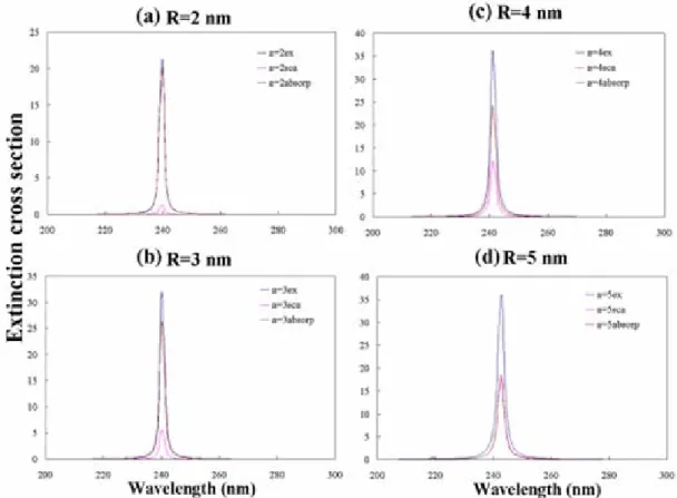
(11) 2.3.6. Electrically controlled light scattering .....................................................31. 2.3.7. Enhanced semiconductor optical absorption ...........................................32. 2.3.8. Bio-sensor device.....................................................................................31. 2.4 Future Development of LSPR ..............................................................................34 Chapter 3 Theoretical backgraund ...............................................................................38 3.1 Plasmon damping in metal ...................................................................................39 3.2 Optical Dielectric Property of metal material ......................................................39 3.2.1 Dielectric response in quasi electric field ..................................................41 3.2.2 Oscillation via an incident electromagnetic radiation .................................45 3.2.3 Theoretical and Experimental optical constant ...........................................45 3.3 Mie’s theory..........................................................................................................49 3.3.1. Dielectric dependent absorbance .............................................................52. 3.3.2. Scattering, absorption and extinction cross section ....................53. 3.4 Separation of plasmon-polariton modes of metal particle .................................54 Chapter 4 Real time absorbance spectra of silver nano-particles film.........................57 4.1 Optical absorbance of silver nanoparticle ............................................................57 4.1.1. Dielectric and size dependent absorbance ...............................................58. 4.2 Preparation of silver nanoparticles film ...............................................................59 4.3 Micro-observation of sliver nanoparticles film....................................................60 4.4 Real time observation on the evolution silver nanoparticles film........................62 4.4.1. Dark-field microscopy .............................................................................62. 4.4.2. Real time optical absorbance spectra.......................................................64. Chapter 5 Laser pulse induced gold nanoparticles gratings.........................................69 5.1 Deposition of nano thick gold film ......................................................................69 5.2 Transfromation between optical and thermal energy ...........................................71 5.3 Gold nanoparticles gratings..................................................................................73 VII.
(12) 5.3.1. Diffraction property of gold nanoparticles gratings.................................74. Chapter 6 Surface plasmons induced extra diffraction band of cholesteric liquid crystal gratings ..............................................................................................79 6.1 Fundamental optical property of chlesteric liquid crystal....................................79 6.1.1. Optical birefringence .............................................................................79. 6.1.2. Theoretical Diffraction efficiency of CLC grating ................................80. 6.1.3. Diffraction pattern and diffraction efficiency ........................................83. 6.2 Surface plasmon effect induced by CLC grating environment ............................86 6.2.1. Fabrication of CLC grating with Ag nanoparticles................................87. 6.2.2. Extra diffraction band induced by surface plasmon effect ....................89. 6.3 Theoretical model of periodic surrounding environment.....................................91 Chapter 7 Summmary ................................................................................................101 Appendix: Optical property of liguid crystal .............................................................103 List of Publication......................................................................................................112. VIII.
(13) List of Figures Figure 2.1: Rayleigh light-scattering of particles deposited on a microscope glass slide. The slide is used as a planar waveguide, which is illuminated with a tungsten source. The image was taken with a digital camera........................................8 Figure 2.2: Dependence of color on shape lead to a big variation of resonant wavelength. .....................................................................................................9 Figure 2.3: Extinction scattering of gold nanoparticles was sensitive to the dielectric constant of solution environment....................................................................9 Figure 2.4: (a) absorption spectrum of a gold nanorod sample with an average aspect ratio of 3.3. The band at 525 nm is referred to as the transverse plasmon resonance, while the one centered at 740 nm is the longitudinal plasmon absorption. (b) TEM image...........................................................................10 Figure 2.5: Theoretical absorbance spectra of metal nanorod with various aspect ratios and surrounded in environment with various dielectric constants................11 Figure 2.6: (a) A seed-mediated growth for gold and silver nanorods and nanowires. (b) TEM of gold nanorods, aspect ratio 18, made by the seed-mediated growth approach............................................................................................12 Figure 2.7: Aqueous solutions of silver nanorod show (A) absorbance spectra and (B) a beautiful variation in visible color depending on the aspect ratio of the suspended nanoparticles. : (a)-(f) silver nanorods of aspect ratio 1-10. .......12 Figure 2.8: Two basic approaches to nanomaterials fabrication: top-down (from left to the right) and bottom-up (from right to the left). ..........................................13 Figure 2.9: (A) Three distinctive stages are identified in nanoprism formation: induction, growth, and termination. (B) Time-dependent UV-Vis spectra showing the conversion of silver nanospheres to nanoprisms (a) before. IX.
(14) irradiation and after (b) 40, (c) 55, and (d) 70 hours of irradiation. .............14 Figure 2.10: TEM images (reverse print) mapping the morphology changes (A) before irradiation and after (B) 40, (C) 55, and (D) 70 hours of irradiation. Except for the inset in (A), the scale bar is 200 nm for all four images. ..................15 Figure 2.11: (a) A SEM of hexagonal array of dots. (b) The energies of the upper and lower branches of the SPP energy gap as a function of the propagation direction. .......................................................................................................16 Figure 2.12: (a) SEM image (aken at an angle of 52°) of circular nanoslits of 7.55 um diameter and 140 nm width. (b) Schematic of the NSOM setup. (c) NSOM image of the SPP interference pattern at λlight=568 nm. ...............................17 Figure 2.13: A silver nano-hole array fabricated by FIB system ...............................17 Figure 2.14: (a) Normal incidence transmission image and (b) spectra for the subwavelength hole-arrays............................................................................18 Figure 2.15: Surface-enhanced Raman spectra of R6G obtained with a linearly polarized confocal laser beam. When polarization direction is parallel to the long axis of particle, the weak signal can be enhanced via the excitation of surface plasmons on Ag nanopartilces..........................................................20 Figure 2.16: (a) Investigation of surface plasmon interactions with a four-particle, photo tunneling image model Forbidden light scan image for the configuration (b) Experimental images recorded with aperture SNOM. Forbidden light scan image (left) and shear-force scan image (right). The parameters of the layered reference system correspond to those of the theoretical model...........................................................................................21 Figure 2.17: (a) Photograph of 20 nm diameter Au and Ag rods. The two labeled rods are typical of the ones used for these experiments. (b) Optical microscope image of a 4.7mm long Au rod exposed to through-prism TIR illumination at X.
(15) 532 nm. Note the strong scattering at the rod input and the absence of scattering at distal tip. (c) Image of the same Au rod under TIR illumination at 820 nm. Under these conditions, both ends of the rod exhibit strong emission/scattering. (d)-(e) A 4.7mm long Ag rod illuminated at 532 and 820 nm, respectively. Emission is observed from both tips at both wavelengths in the case of Ag. .....................................................................23 Figure 2.18: Two-dimensional spatial images of the electric field intensity in a plane through the particle centers of four Ag nanospheres with interparticles spacing of (a) 4 nm, (b) 2 nm, and (c) 1 nm at resonant excitation. ...........24 Figure 2.19: Distribution of the longitudinal component of the electric field in the vicinity of an array of 12 Ag particles with 10 nm diameter, illustrating two distinct modes. In panel (a), an antennalike mode resembling that of a single elongated wire is excited resonantly at 0.35 eV; in panel (b), a coupled-particle-like mode resembling that of a chain of independent particles is excited resonantly at 1.65 eV. The slight axial asymmetry of the filed distribution is caused by superposition of the resonant mode with the exciting plane wave.......................................................................................25 Figure 2.20: Bird’s eye view of a nanodot coupler with a SPP condenser. (b) Experimental system. (c) Schematic illustration of the SPP condenser. ......27 Figure 2.21: (A) Fabrication of the nanodot coupler and SPP condenser: (a) Anodic bonding, (b) carbon hemisphere deposition using FIB, (c) 120 nm gold film deposition using sputtering, (e) and (d) SEM images of the fabricated nanodot coupler and SPP condenser. (B) (a) Shear-force image of the SPP condenser. (b) The near-field energy distribution of sad taken at l=785 nm. (c) Calculated spatial distribution of the electric-field energy using the FDTD method. The dashed and solid curves in (d) are cross-sectional XI.
(16) profiles along the dashed white lines in (b) and (c), respectively.................28 Figure 2.22: (A) Experimental setup: sketch of the nanoscale surface structures combined with an atomic force microscope image of the sample surface. The double arrow indicates the polarization direction of the incident light. (B) (a) (b) and (c) (d) show beam-splitter and reflector functions. ..........................29 Figure 2.23 (a): Sample assembly for QD SPCE measurement. The glass slide with the sample was attached to the hemispherical glass prism using an index-matching fluid. Two cones of directional radiation enter the coupling prism at slightly different angles. The QD’s orange SPCE radiates inside a narrow green cone of directional scattered excitation. .................................30 Figure 2.23(b): Angular distribution of 514-nm excitation transformed to a polarized directional radiation of the same wavelength. Essentially, the surface plasmons cannot be excited in the RK configuration by the incident light beam from the air. Observed cones of 514-nm radiation are due to the imperfections of the sample layer (roughness). Whereas the PVA itself does not introduce any significant roughness (compare top and middle panels), the presence of QDs causes a many-fold increase in the 514-nm directional radiation. .......................................................................................................30 Figure 2.24: (a) Gold nnaopartilces are illuminated with white light using a dark-field condenser (b) Scattering spectra of the same single nanoparticle in air (dashed line) and covered with the LC (solid line) at an analyzer position of 180 degree.....................................................................................................32 Figure 2.25: (a) Schematic diagram of Si p-n junction diode device structure with metallic nanoparticles. (b) the extinction efficiency is dependent on the particle size. ..................................................................................................33 Figure 2.26: (a)Schematic representation of the method. Single-stranded DNA was XII.
(17) self-assembled onto gold nanoislands on a glass slide with the subsequent introduction of mercaptohexanol spacer molecules (short thiols in the figure) and then hybridized by the complementary DNA. (b) T-SPR spectra of gold nanoislands is prior to (1) after the self-assembly of single-stranded DNA, (2) mercaptohexanol and hybridization by the complementary DNA unlabeled, and (3) by gold nanoparticles........................................................................34 Figure 3.1: (a) Metal nanoparticle is probed by a incident light and then irradiates scattering light. (b) the scattering light from Ag nanopartilces in dark-field microscopy....................................................................................................39 Figure 3.2: Energy relaxation of a surface plasmon. The relaxation takes place either via radiative or non-radiative processes. The nonradiative relaxation channel leads to the creation of electron-hole pairs and the subsequent relaxation into hot electrons and phonons.............................................................................39 Figure 3.3: (a) A damped oscillation in time corresponds via the Fourier transformation to (b) a broad peak in the frequency spectrum. ....................40 Figure 3.4: Space charge separation in a slab due to the displacement of the electron gas relative to the ionic crystal lattice .........................................................42 Figure 3.5: Space charge separation in an ellipsoid of revolution...............................43 Figure 3.6: Depolarization factor Qa and Qc vs c/a, where c and a are semi-axes of the ellipsoid of revolution. c is the semi-axis of the axis of revolution. Qc is the depolarization factor for electric field in the direction of the axis of revolution. .....................................................................................................44 Figure 3.7: When the box is larger than the wavelength, the periodic variation of the space charge separation leads to no net restoring force for the whole electron gas. ................................................................................................................46 Figure 3.8: (a) Real and (b) imaginary part of the dielectric function of silver .........48 XIII.
(18) Figure 3.9: (a) Real and (b) imaginary part of the theoretical dielectric function and Johnson’s measurement. ...............................................................................48 Figure 3.10: Extinction cross section of Au nanoparticle with a radius of 50 nm, three high orders plasmon modes can be found in the spectra (n=1).....................51 Figure 3.11: Extinction cross section of Au nanoparticle with a radius of 50 nm, three high orders plasmon modes can be found in the spectra (n>1).....................51 Figure 3.12: Comparison of experimental absorbance and theoretical extinction cross section of Ag spherical nanoparticle.............................................................52 Figure 3.13: Extinction cross section of Au spherical nanoparticle in various radius from 40 to 70 nm...........................................................................................53 Figure 3.14: Extinction cross section is a function and varies with the dielectric property .......................................................................................................54 Figure 3.15: Extinction, absorption, and scattering cross section vary with the particle radius from 2 to 5 nm....................................................................................55 Figure 3.16: Extinction, absorption, and scattering cross section vary with the particle radius from 6 to 9 nm....................................................................................55 Figure 4.1: Scanning electron micrographs of silver nano-particles film at every annealing step................................................................................................62 Figure 4.2: Atomic force micrographs of silver nano-particles film at every annealing step. ...............................................................................................................62 Figure 4.3: (a) Dark-field micrograph of silver nanoparticles in various sizes. (b) Collecting the scattering light with dark-field objective...............................63 Figure 4.4: Dark field optical micrographs of silver nano-particles film at every annealing step................................................................................................64 Figure 4.5: Experimental setup for absorbance spectra measurement .......................65 Figure 4.6: Real time absorbance spectra of silver nano-particles film at various XIV.
(19) heating temperature of 28, 50, 100, 150, 200, and 250 ℃. A broad peak appeared at around 552 nm (100 ℃) and then shifted to shorter wavelength band at around 500 nm (250 ℃). ..................................................................65 Figure 4.7: Absorbance spectra at the heating temperature of 250 and 300 ℃, then the temperature was kept at 300 ℃ for an hour. The absorbance peak (500 nm at 250 ℃) shifted to longer wavelength band around 572 nm (300 ℃ after an hour)..............................................................................................................66 Figure 4.8: Variations of the peak position and the full width half maximum of the absorbance spectra at every annealing step. .................................................67 Figure 5.1: Fabrication process of nano thick gold film on PMMA substrate ..........71 Figure 5.2: (a) Experimental and (b) theoretical absorbance spectrum of gold film...71 Figure 5.3: Experimental setup for the formation of nano-particle grating via a spatially periodic heating process on a thin gold film. The periodic intensity pattern is obtained via the interference of two Nd-YAG pulse beams. ........72 Figure 5.4: Spatial distributed optical density and temperature along interference pattern. ..........................................................................................................73 Figure 5.5: Spatial distribution of the surface temperature due to the periodic variation of the incident beam intensity on the gold film. ...........................................74 Figure 5.6: (a) Scanning electron and (b) dark-field optical micrograph of gold nano-particle gratings induced with a Nd-Yag laser pulse with a fluence of 70 mJ/cm2......................................................................................................75 Figure 5.7: (a) Scanning electron and (b) dark-field optical micrograph of gold nano-particle gratings induced with a Nd-Yag laser pulse with a fluence of 110 mJ/cm2....................................................................................................75 Figure 5.8: First order diffraction efficiency of gold nano-particle gratings as a function of probe wavelength. ......................................................................76 XV.
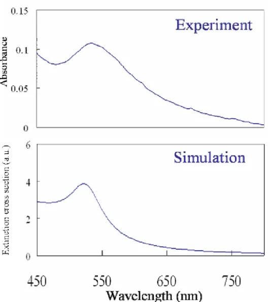
(20) Figure 5.9: Absorbance of a thin layer of gold nanoparticles with a size (diameter) of ~100 nm. The insert shows the SEM of an array of gold nano-particles distributed on the PMMA layer. ...................................................................77 Figure 6.1: Optical birefringence property of liquid crystal is dependent on the light polarization .................................................................................................81 Figure 6.2: Different angle between polarization and LC molecule lead to a variation of effective refraction index..........................................................................81 Figure 6.3: With an application of a proper voltage, an ideal cholesteric liquid crystal grating is constructed in the CLC cell...........................................................81 Figure 6.4: CLC grating was probed by a Nd-YAG laser of 532 nm, the calculated efficiency of ±4 diffraction order was shown in below. ..............................84 Figure 6.5: Diffraction efficiency of the CLC grating probed by a polarized beam in spectral range from 450 to 750 nm. ..............................................................85 Figure 6.6: First order diffraction efficiency was calculated with respect to the polarization of 0, 30, 60, and 90 degree........................................................86 Figure 6.7: (a) and (b) show the SEM pictures of silver thin films before and after annealing. (c) The AFM picture of the annealed film shows the size of silver nano-particle is ~50 nm. ...............................................................................89 Figure 6.8: (a) Cholesteric liquid crystal cell with silver nanoparticles distributed on one plate of the cell, (b) the CLC grating structure well-formed with the application of a proper voltage to the cell.....................................................90 Figure 6.9: Cholesteric liquid crystal grating structure was observed with an optical microscope and the diffraction pattern shown in the top (probed by the He-Ne laser of 632.8 nm)..............................................................................91 Figure 6.10: Experimental setup for measuring the first-order diffraction of the CLC grating. ..........................................................................................................91 XVI.
(21) Figure 6.11: The first-order diffraction efficiency versus wavelength of the CLC grating with and without the silver nanoparticles distributed on one plate of the cell, and the absorbance of the silver nanoparticles covered with E7 liquid. crystal is shown in the insert illustration. ......................................93. Figure 6.12: Theoretical absorbance of silver nanoparticles surrounded by the environment with refractive indices of 1.52 and 1.74. The insert shows the silver nanoparticles layer was posited between the CLC grating and ITO plate. The particles experienced the environments with index of ne and no. 97 Figure 6.13: Theoretical diffraction efficiencies show the extra diffraction band of CLC grating with silver nanoparticles. .........................................................98 Figure A1: liquid crystalline mesophases between the solid and isotropic liquid phase .....................................................................................................................104 Figure A2: rodlike LC molecule (5CB) and different views of scientists. ................105 Figure A3: Phase of liquid crystal (a) smectic phase; (b) nematic phase; (c) cholesteric phase. ..........................................................................................................106 Figure A4: angle difference between director and individual LC molecule ............106 Figure A5: Optical birefringence of LC material is dependent on the light wave vector. .....................................................................................................................108 Figure A6: Three types of orientation change. ..........................................................108 F igure A7: Dielectric property of LC material. ........................................................109 Figure A8: Under an electric field, the reorientation of LC molecules is dependent on the dielectric anisotropic property. .............................................................110. XVII.
(22) List of Tables Table3.1: Depolarization factor due to various shape of particle……………….........44 Table3.2: Decomposition of the extinction of spherical metal particles into true absorption and scattering losses of various multipolar modes…….............56 Table5.1: Physical thermal properties of gold material at 25 ℃……………….........73 Table A1: Rodlike Liquid Crystal Materials…………………………….…….........105 Table A2: S parameter of various matter phases………………................................107. XVIII.
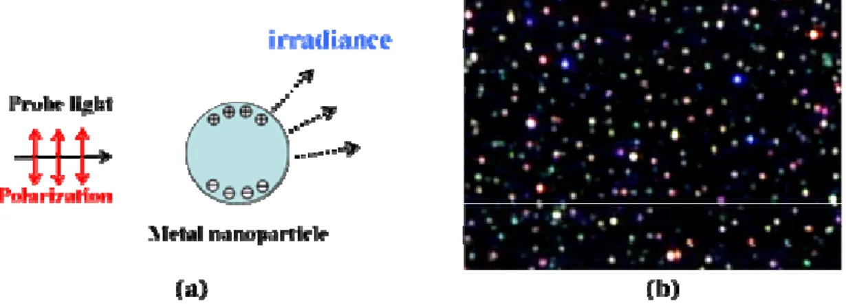
(23) Chapter 1 Introduction 1.1 Background Localized surface plasmons of metal nanoparticles exhibit interesting and particular optical properties. Fundamental optical property is dependent on the excitation of collective electron oscillation in metal nanoparticles [1-5]. The electron motion induced by the external electromagnetic field dominates the optical dielectric of metal material, and then affects the resonance wavelength and intensity of the scattering and absorption. In the comparison of optical response due to the collective electron motion in metallic nanoparticle, the electromagnetic response of a metal nanosphere due to an exciting field can be estimated by solving Maxwell’s theory. Mie first applied the analytical solution of spherical particles in a homogeneous medium to a problem of light scattering and absorption. It is the famous Mie theory. Surface plasmons are limited at the interface between the metal and the dielectric material, when it is excited by the optical field. The study in the surface plsmon resonance is classified into two different metal structures, and they are planar metal film and metallic nanoparticles. The plasmons confined at the metal-dielectric interface and on metallic nanoparticles are called “surface plasmon” and “localized surface plasmon”, respectively. For a particle with a diameter larger than about 10 nm, the dielectric property is known to be like bulk material and to be size dependent. Following classical electrodynamics, the optical response of large individual metal particle can be calculated. For small particles, the optical dielectric is a function of particle size. A large number of studies show the electronic structure of metal nanoparticle. It is well known that the excitation of localized surface plasmon resonance is. 1.
(24) determined by the shape, size, size distribution, and dielectric property of surrounding environment of nano-structured metal [6-10]. Upon the dependence of these factors, various applications are developed rapidly. Surface enhance Raman scattering has been applied to detect weak signal from single molecule. Biosensor is developed based on the dependence of dielectric property of outside environment on resonant wavelength [11-13]. In addition, many nano-scale devices based on localized surface plasmon effect, for example, plasmon-mirror, beam-splitter, coupler and condenser, have been realized for potential optical integral circuit application [14-20]. In addition, the development of nano-technology or equipments for the nano-structure fabrication of equipment also play very important role to the study of localized surface plasmons emerged from metal nanoparticles. These include chemical synthesis and photolithography with precise control of the metal nano-structure system. This development leads to a significant increase in the studies of the physical properties of nano-optical systems. More and more nano-technologies have been proposed to the construction of nano-optical system. The realization of the nano-scale device systems can lead to many interesting phenomena. Such as the interesting optical phenomena of sub-diffraction-limit image, optical signal propagation via metal nanoparticles array, size- and shape-dependent optical spectrum, and dielectric modulating plasmons, can be achieved easily by these fabricating techniques [21-25]. However, the fabricating process of these nano-devices was complex and the devices could not be modulated externally. The function of external modulation (e.g., via liquid crystals) on the nano-devices may be provide potential of flexible operation and modulation on the localized surface plasmons effect. In this study, the real time investigation of the metal nanoparticles film under a high temperature annealing has beenm accomplished. The metal film aggregated 2.
(25) together to form a particle shape. The optical dynamics due to the real time absorbance spectra and dark-field micrograph reveals something special differed from the results proposed by previous works. We also present a simple and fast approach of laser pulse ablating to establish a metal nanoparticles array. Finally, liquid crystal materials, with the outstanding electrical-optical switching and optical birefringence properties, are employed to cover the metallic material as an electrically-switching environment. The reorientation of LC molecule is controlled by applying an electrical field on the cell. 1.2 Motivation Although the localized surface plamson can exhibit particular optical property differed from that of bulk structure, the fabricating process of these nano-devices was complex and the devices could not be modulated externally. A direct and non-destructed observation on nano-structured metal and a simple fabricating process of these nano-devices with metal nano-particles are required to the development of nano-technology. In this study, we try to find a solution to solve the above problems. A real time observation of nanoparticle system, laser pulse induced metal gratings array, and external modulation of surface plasmon effect by using liquid crystal as surrounding environment are investigated in this study. 1.3 Organization This thesis was organized as follows: First, I will briefly review the development on nano-structured metal material or devices in chapter 2. In Chapter 3, the theoretical background was described due to the Mie theory. Chapter 4 mentioned the first work in this study. The topic is “Real time absorbance spectra due to optical dynamics of silver nano-particles film”. In this chapter, we proposed an optical method to observe the dynamic behavior of silver nano-particles film under a heating 3.
(26) treatment. The method exhibit the real time optical information differed from the analysis of SEMs. Chapter 5 focuses on the fast and simple fabrication of metal nanoparticles. By laser pulse ablation, the metal nano-particles can be obtained immediately from a film structure and the nano-particles can be applied in optical nano-device and high order nano-particles structure. Chapter 6 shows an extra diffraction band of cholesteric liquid crystal grating induced by the surface plamons effect. It was noted that the periodic localized surface plasmons were excited due to the CLCs grating environment and to affect the diffraction behavior of intrinsic CLCs grating. The summary of this study is finally concluded in Chapter 7.. 4.
(27) Reference 1. 2. 3. 4.. G. Mie: Ann. Phy. 25, 377 (1908) P. Debye: Ann. Phys. 30. 57 (1909) H. C. Van de Hulst, “Light Scattering by Small Particle”, Wiley, New York (1957) Willam T. Doyle, “Electrodynamic resoponse of metal spheres”, J. Opt. Soc. Am.. A 2, 1031 (1985) 5. U. Kreibig, M.Vollmer, Ootical Properties of Metal Cluster, Springer-Verlag, Berlin, New York (1995) 6. S. Underwood, P. Mulvaney, Langmuir, 10, 3427 (1994) 7. P. Mulvaney, Langmuir, 12, 788 (1996) 8. Eliza Huntter and Janos H. Fendler, “Exploitation of Localized Surface Plamon Resonance”, Adv. Mater. 16, 1685 (2004) 9. Rongchao Jin,1 YunWei Cao,1 Chad A. Mirkin,1 K. L. Kelly,George C. Schatz,1 J. G. Zheng, “Photoinduced Conversion of Silver Nanospheres to Nanoprisms”, SCIENCE 294, 1901 (2001) 10. J. J. Mock, M. Barbic, D. R. Smith, D. A. Schultz, and S. Schultz, “Shape effects in plasmon resonance of individual colloidal silver nanopaticles”, Journal of Chemical Physics 116, 6755 (2002) 11. Katrin Kneipp, Yang Wang, Harald Kneipp, Lev T. Perelman, Irving Itzkan, Ramachandra R. Dasari, and Michael S. Feld, Phys. Rev. Lett. 78, 1667 (1997) 12. Eliza Hutter and Marie-Paule Pileni, “Detection of DNA Hybridization by Gold Nanoparticle Enhanced Transmission Surface Plasmon Resonance Spectroscopy”, J. Phys. Chem. B 107, 6497( 2003) 13. YunWei Charles Cao, Rongchao Jin, Chad A. Mirkin, “Nanoparticles with Raman Spectroscopic Fingerprints for DNA and RNA Detection”, Science 297, 1536 (2002) 14. P. Dawaon, A. F. Puygranier, J. P. Goudonnet, Phys. Rev. B 63, 205410 (2001) 15. Robert M. Dickson and L. Andrew Lyon, “Unidirectional Plasmon Propagation in Metallic Nanowires,” J. Phys, Chem. B 104, 6095 (2000) 16. L. A. Sweatlock, S. A. Maier, and H. A. Atwater, “Highly confined electromagnetic fields in arrays of strongly coupled Ag nanoparticles”, Physical Review B 71, 235408 (2005) 17. H. Yockelllelievre, E. F. Borra, A. M. Ritcey, L. V. Dasilva, Appl. Opt. 42, 1882 (2003) 18. Stefan A. Maier, Mark L. Brongersma, Pieter G. Kik, and Harry A. Atwater, “Observation of near-field coupling in metal nanoparticle chains using far-field polarization spectroscopy” PHYSICAL REVIEW B 65, 193408 (2002) 19. Wataru Nomura, Motoichi Ohtsu, and Takashi Yatsui, “Nanodot coupler with a 5.
(28) surface plasmon polariton condenser for optical far/near-field conversion”, Appl. Phys. Lett 86, 181108 (2005) 20. H. Ditlbacher, J. R. Krenn, G. Schider, A. Leitner, and F. R. Aussenegg, “Two-dimensional optics with surface plasmon polaritons”, Appl. Phys. Lett. 81, 1762 (2002) 21. G. Kalyuzhny, A. Vaskevich, M. A. Schneeweiss, and I. Rubinstein, Chem. Eur. J. 8, 3850 (2002) 22. G. Kalyuzhny, M. A. Schneeweiss, A. Shanzer, A. Vaskevich, and I. Rubinstein, J. Phys. Chem. B 104, 8238 (2001) 23. E. Hutter, M. P. Pileni, J. Phys. Chem. B 107, 6497 (2003) 24. M. Maillard, P. Huang, L. Brus, Nano Lett 3, 1611 (2003) 25. R. C. Jin, Y. C. Cao, E. C. Hao, G. S. Metraux, G. C. Schatz, C. A. Mirkin, Nature 425, 487 (2003). 6.
(29) Chapter 2 Study and application of metallic nanoparticles system Collective electron oscillation, localized surface plsmons, can be easily excited by light. The particular optical property due to the surface palsmon effect has been explored based on the electrodynamics of conduction electrons in metal nanoparticles. Since wavelength dependent scattering varies with the shape, size, and even environment dielectric property of metal nanoparticles, a wild application, such as photonics, sensors, signal enhancement of local electromagnetic filed, are rapidly studied and developed. Recent studies and applications of localized surface plasmons are reviewed here. In this chapter, a brief survey of fundamental characteristics of LSP is introduced first. Many outstanding experimental and theoretical works present the dependence of the geometry and dielectric property of metal nanoparticles on the localized surface plasmon resonance. In the following section, I will mention various applications of metal nano-structure system, such as surface enhanced Raman scattering, light propagating channel, mirror, condenser, biosensor, and so on. Finally, a future development of LSPR will be given. 2.1 Fundamental optical property of metal nano-particles It is well known that the localized surface plasmon resonance is dependent on the size, shape, dielectric property of metal nanoparticles. The collective electron oscillation confined in the metal nanoparticles determines the particular optical property differed from bulk material. 2.1.1 Geometry effect on localized surface plasmons Rongchao Jin shows that the metal nanoparticles can exhibit various bright colors due to different geometry. The bright colors of noble metal nanoparticles (silver and gold) are due to the excitation of resonant collective oscillation of the free. 7.
(30) electrons in the particles. Figure 2.1 shows that the gold and silver nanonparticle scattered light in particular band and various color dots can be observed in dark field microscopy. First, to compare A with D Ag nanoparticle, the particle excites red and wathet-blue colors, respectively, under the shape effect (triangular and sphere). In the other set of B and C particle (Au spherical particle with size of 100 and 50 nm, respectively), exhibited yellow and green colors, referred to the size effect. Since the collective electron oscillation is strongly dependent the size and shape of metal nanoparticles (geometry determines the oscillating behavior of electron in metal particles) and resulting the variation of the electron damping relation, thus the resonance wavelength was altered by these factors. The interesting dependent of particle size and shape on localized surface plasmon resonance will be detail discussed in next chapter.. Figure2.1: Rayleigh light-scattering of particles deposited on a microscope glass slide. The slide is used as a planar waveguide, which is illuminated with a tungsten source. The image was taken with a digital camera. [2]. In addition, the shape effect also determines the optical scattering spectra of metal nanoparticles. As shown in Figure 2.2, the particle in various shapes of sphere, triangular, and pentagon lead to a big shift of optical resonance wavelength. The wavelength shift of 325 nm is exhibited between the spherical and triangular metal particles. 8.
(31) Figure 2.2: Dependence of color on shape lead to a big variation of resonant wavelength. [3]. 2.1.2 Dielectric effect on localized surface plasmons Furthermore, the extinction scattering due to the excitation of localized surface plasmons is also strongly dependent on the dielectric property of surrounding environment. Figure 2.3 presents that the scattered particular light band can be observed be immersing gold nanoparicle with a diameter ~16 nm in the solution of refractive index (from left to right, 1.336, 1.407, 1.481, 1.525, and 1.583). It is noted that the scattering light shifted to longer wavelength when the index is increasing.. Figure 2.3: Extinction scattering of gold nanoparticles was sensitive to the dielectric constant of solution environment. [4]. 9.
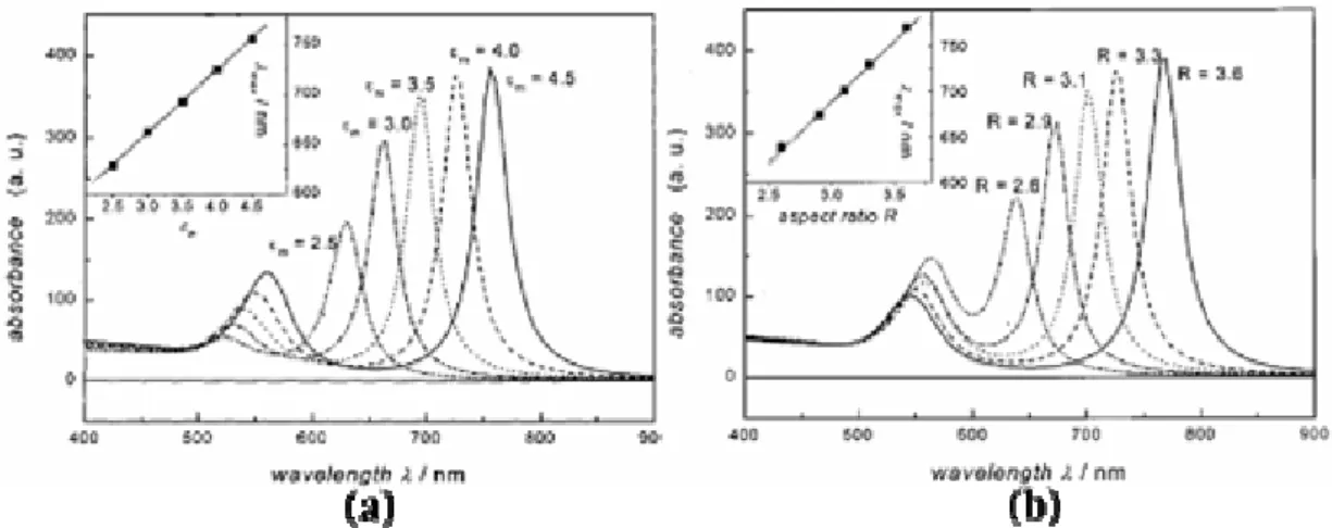
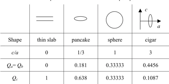
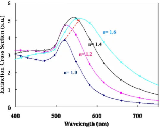
(32) 2.1.3 Localized Surface Plasmon of Metal Nanorod At present, so many factors, such as size, shape, and dielectric effect, affected localized surface plasmon resonance were rapidly reviewed. However, the other factor of aspect ratio of metal nanorod also leads to an interesting optical property of metal nanopart. In S. Link’s work, he presents that the aspect ratio of gold nanorod significantly affects the optical property of localized surface plasmon. Two different excited plasmons modes, transverse and longitudinal mode, are found on the metal nanorod. In Figure 2.4 (a), the absorption spectrum shows two absorption maxima at 525 and 740 nm corresponding to two different modes. This is because the absorption of visible light both along the direction of the nanorod length (the longitudinal plasmon band) and along the direction of the nanorod width (the transverse plasmon band). Figure 2.4 (b) is the transmission electron micrograph (TEM) image of nanorods with average aspect ratio of ~3.3. A well control aspect ratio of nanorod has be done in this work.. Figure 2.4: (a) absorption spectrum of a gold nanorod sample with an average aspect ratio of 3.3. The band at 525 nm is referred to as the transverse plasmon resonance, while the one centered at 740 nm is the longitudinal plasmon absorption. (b) TEM image [6]. Although two different surface plasmon modes are excited due to the geometry of nanorods, the absorbance property due to dielectric variation seems to be the same. 10.
(33) with that of metal spherical nanoparticles. The resonance wavelength shifts to red when increasing the dielectric constant of surrounding environment. In Figure 2.5 (a) and (b), the theoretical dielectric and aspect-ratio dependent absorbance spectra of metal nanorod are shown. By increasing the environment dielectric constant and the aspect ratio of metal nanorod, the maximum absorbance in the spectra shifts to red band. This characteristic determined the macroscopic optical property and that provides a potential to externally modulate the localized surface plasmon effect.. Figure 2.5: Theoretical absorbance spectra of metal nanorod with various aspect ratios and surrounded in environment with various dielectric constants. [6]. Besides the above theoretical analysis, Catherin J. Murphy and Nikhil R. Jana proposed an experimental observation of aspect-ratio dependent optical absorbance spectra. In this experiment, a seed-mediated growth approach is used to make metallic nanorods and nanowires in homogeneous solution. Figure 2.6 (a) shows the evolution begins with the synthesis of metallic nanospheres by chemical reduction of a metal salt with a strong reducing agent such as sodium borohydride. Citrate is employed as a capping agent to prevent particle growth. The gold or silver spheres with diameter of 3-5 nm are generated and become as seeds to grow more anisotropic nanostructures. Figure 2.6 (b) is the transmission electron micrograph (TEM) of the gold nanorods with an aspect ratio of 18. 11.
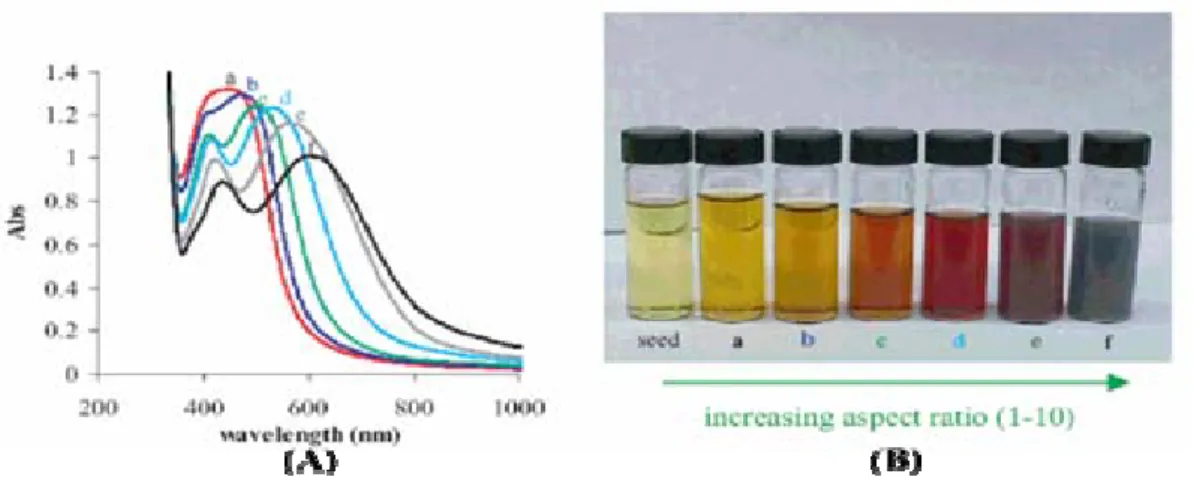
(34) Figure 2.6: (a) A seed-mediated growth for gold and silver nanorods and nanowires. (b) TEM of gold nanorods, aspect ratio 18, made by the seed-mediated growth approach. [7]. This seed-method provides a very good control of the aspect ratio of metal nanorod. As shown in figure 2.7 (a), the maximum absorbance shifted to longer wavelength as increasing the aspect ratio of metal nanorods. This variation of absorbance spectra lead to various scattering light due to aspect ratio. The result confirms the theory prediction.. Figure 2.7: Aqueous solutions of silver nanorod show (A) absorbance spectra and (B) a beautiful variation in visible color depending on the aspect ratio of the suspended nanoparticles. : (a)-(f) silver nanorods of aspect ratio 1-10 [7].. In summary, there are so many factors, such as geometry and dielectric property of surrounding environment, significantly affect the excitation of localized surface plasmons on the metallic nanoparticle and leading to the particular optical property. On the base of these advantages, high potential of sensor and classifying applications, can be accomplished simply.. 12.
(35) 2.2 Preparation and Arraying of metal material There are two general ways available to produce nano-structure materials. As shown in Figure 2.8, the first way is to start with a bulk material and then piece it into smaller fragments via using mechanical, chemical or other form of energy (top-down). The opposite approach is to synthesise the material from atomic or molecular species by chemical reactions, allowing for the precursor particles to grow and become bigger size (bottom-up). Most of the researchers are interested to well control of particle size, shape, size distribution, particle composition, and the degree of particle agglomeration. In this section, we will review three previous works included the fabrication of metal nanoparticles and metal nano-array.. Figure 2.8: Two basic approaches to nanomaterials fabrication: top-down (from left to the right) and bottom-up (from right to the left).. 2.2.1 Photoinduced conversion of silver naonspheres to nanoprisms In general, spherical silver particles are prepared by injecting NaBH4 solution to an aqueous solution of AgNO3, with a presence of trisodium citrate. Bis(p-sulfonatophenyl) phenylphosphine dihydrate dipotassium salt solution (BSPP) is subsequently added by drop-wise addition to the solution as a particle stabilizing agent. After the radiation of the conventional fluorescent light, the metal nanoparticle can be produced in the solution. 13.
(36) Rongchao Jin presented a time-dependent spectroscopic observation correlated with TEMs of silver nanoparticles. In Fig. 2.9 (a), we can find that the initial silver particles (~8 nm) are converted from spherical to triangle structure. During the initial stages of growth, both spheres and prisms exist at the same time. After 70 hours, most of the initial spheres (.99%) are converted to the prismatic structures. In this growth reaction, they also observed a set of color changes of the sample. Initially, the solution is yellow and then turned green and finally blue in whole growth of 70 hours. From the analysis time dependent extinction spectrum in Fig. 2.10 (B), a decrease in intensity of the surface plasmon band at λmax = 400 nm (for the spherical particles) was turned to a growth of three new bands of λmax = 335 (weak), 470 (medium), and 670 nm (strong), respectively. After 70 hours, the band at 400 nm completely disappeared. This optical response also implied the growth evolution of silver nanoparticle from spherical to triangle shape.. Figure 2.9: (A): Three distinctive stages are identified in nanoprism formation: induction, growth, and termination. (B) Time-dependent UV-Vis spectra showing the conversion of silver nanospheres to nanoprisms (a) before irradiation and after (b) 40, (c) 55, and (d) 70 hours of irradiation. [2]. In Figure 2.10 (a) and (d), TEM pictures shows the whole growth of nanoparticles. Size and population of the Ag prisms increase with time and a concomitant decrease in the number of spherical particles can be found. Figure 2.10 (D) shows the most of nanoparticles turned to triangle shape. These data clearly show 14.
(37) that the silver nanoprisms evolve from the initial spherical nanoparticles. This work proposes a detail time dependent observation on the evolution of photoinduced chemical synthesis and that leads to a advance understanding of chemical synthesis mechanism.. Figure 2.10: TEM images (reverse print) mapping the morphology changes (A) before irradiation and after (B) 40, (C) 55, and (D) 70 hours of irradiation. Except for the inset in (A), the scale bar is 200 nm for all four images. [2]. 2.2.2 Electron beam lithography (nano-array) Electron beam lithography is employed a beam of electrons to scan in a pattern a resistant surface and the pattern can be transferred on the sample surface by the selectively removing either exposed or non-exposed regions of the resist. The purpose is to create very small structures and to create very nano-scale electronic devices. The primary advantage of electron beam lithography is to beat the diffraction limit of light and make features in the nano-scale regime. This form of maskless lithography has found wide usage in mask-making for photolithography, low-volume production of semiconductor components, and research and development. Figure 2.11 shows a two-dimensional photoresist dot array covered by a thin silver film. The pattern was prepared by an e-beam lithography system. This approach provides a precise control of array structure in and a good band gap property can be obtained as this photonic device. By altering the factors, such as spacing and size of the metal dots, of this nano-array, the band gap can be modulated for certain purpose in optical photonic application. 15.
(38) Figure 2.11: (a) A SEM of hexagonal array of dots. (b) The energies of the upper and lower branches of the SPP energy gap as a function of the propagation direction. [9]. 2.2.3 Focused ion beam (FIB) Focused ion beam (FIB) is inherently destructive to the specimen. When a high-energy gallium ion-beam strikes the sample, the atoms are sputtered from the surface. FIB, like e-beam lithography, is often used in the semiconductor industry to patch or modify an existing semiconductor device. For example, in an integrated circuit, the gallium beam could be used to cut unwanted electrical connections, or to deposit conductive material for a connection. In the surface plasmon study area, FIB is a good tool to fabricate a metal nano-structure or metal array. V. Vlasko-Vlasov uses FIB system to fabricate Ag circular nanoslits with width of 140 nm and diameter of 7.55 um, as shown in Fig. 12(a). The circular nanoslits excite strong surface plasmon polaritons (SPPs), resulting a very interesting interference patterns due to plasmons emitted from opposite sides of the circle. The sample is illuminated from the bottom by a tunable gas laser generating a series of sharp lines between 476 and 676 nm. The resulting SPP interference patterns were imaged by a near-field scanning optical microscope (NSOM) with a 50 nm fiber aperture (Figure 2.12 (b)).. 16.
(39) Figure 2.12: (a) SEM image (aken at an angle of 52°) of circular nanoslits of 7.55 um diameter and 140 nm width. (b) Schematic of the NSOM setup. (c) NSOM image of the SPP interference pattern at λlight=568 nm. [10]. Figure 2.12 (b) illustrates a typical NSOM picture of the plasmon intensity. The obvious interference pattern presents the existence of SPP. NSOM images are largely a representation of the in-plane electric field intensity on the surface of the film. The interference pattern has a period equal to half the SPP wavelength, λSPP/2, the usual period of the standing wave intensity. With decreasing frequency the period increases, however, remaining always smaller than λlight /2. The FIB approach to precisely fabricate metal nano-structure leads to an advance study for localized surface plasmon effect. A precise hole-array can also be fabricated by FIB. Figure 2.13 shows a gold hole-array with a diameter and spacing of 300 nm and 400 nm, respectively.. Figure 2.13: A silver nano-hole array fabricated by FIB system 17.
(40) In Figure 2.14, the transmission spectra of hole-arrays display peaks that can be tuned by adjusting the period and the symmetry. For the blue, green and red arrays, the periods were 300, 450 and 550 nm, respectively, the hole diameters were 155, 180 and 225 nm and the peak transmission wavelengths 436, 538 and 627 nm. The arrays were made in a free standing 300 nm thick silver film.. Figure 2.14: (a) Normal incidence transmission image and (b) spectra for the subwavelength hole-arrays. [11]. In summary, the development of nano-technology promotes the advance of metal nano-structure system. Since the nano-structure can be designed and fabricated in demanded nano-optics device, the optical phenomena of reflection, transmission, propagation, and diffraction, are duplicated in marco-vision optics. The preparations of metal nanoparticle system mentioned in above system provide a easy way to fabricate nano-device for certain purpose. A well control of metal nanoparticle shape can be achieved by chemical synthesis. However, for a complicate metal nanoparticles system, E-beam lithography and FIB is proper to the fabrication of device. Actually, no matter which way to manufactory of optical metal nano-device, a creative idea is essential to advance study.. 18.
(41) 2.3 Application and development of localized surface plasmon resonance (LSPR) In this section, I will introduce the previous works which present the potential application and development of metal nano-device, such as sensor, light channel, condenser, bio-detector, and so on. The realization of these devices not only exhibits interesting physical and chemical phenomena but also leads to a potential for nano-techonology. 2.3.1 Surface plasmon enhanced Raman scattering [12, 13] Due to the weak signal from the molecular structure, it’s difficult to detect the information from the molecular bound. The surface plasmon effect excited on the metallic nano-particles can enhance the signal, known as the surface plasmon enhanced Raman scattering. For this purpose, metallic nanoparticles were widely applied to the observation of weak signal exhibited from molecules. Shuming Nie proposed the Raman spectra of a single rhodamine 6G molecules adsorbed on the selected nanoparticles, the intrinsic Raman enhancement factors were on the order of 1014 to 1015, much larger than the ensemble-averaged values of conventional measurements. This strong enhancement leads to a vibrational Raman signals with more intense and more stable than single-molecule fluorescence. The enhancement of localized electromagnetic field of molecule due to the exciting surface plasmons improves the sensitivity for detection of individual molecule or individual metal nano-particle. Figure 2.14 show the surface-enhanced Raman spectra of R6G obtained with a linearly polarized confocal laser beam from two Ag nanoparticles. The R6G concentration was 2x10-11 M, corresponding to an average of 0.1 analyte molecule per particle. By changing the polarization direction of laser corresponding to the expected particle orientation, the enhanced spectra can be obtained when the polarization parallel to the long axis of particle. All spectra were plotted on the same intensity 19.
(42) scale in arbitrary units of the CCD detector readout signal.. Figure 2.15: Surface-enhanced Raman spectra of R6G obtained with a linearly polarized confocal laser beam. When polarization direction is parallel to the long axis of particle, the weak signal can be enhanced via the excitation of surface plasmons on Ag nanopartilces. [12]. 2.3.2 Interference of locally excited surface plasmons Surface plasmon interaction in a metal nano-slit has mentioned in section 2.2.3. In the following, the SPPs emerged metal nanoparticles also inferred each others and the interference pattern due to the presence of surface plasmons wave can be observed SNOM system. In L. Novotny’s work, a system, shown in Figure 2.15 (a), consists of several protruding particles located on the surface of the layer and the protrusions on the silver layer are considered as small, dipolar silver particles of variable size. The probing particle is locally excited by the monochromatic field Eo. An optical scan image of the surface of the silver layer is obtained by recording the far-field radiation for every position (x,y) of the optical probe. In Figure 2.16 (b), they found a strong iterference of the locally excited surface plasmons revealed by detecting the radiation emitted into the lower half-space at angles beyond the critical angle of total internal reflection. The interference was theoretically investigated via using coupled dipole formalism.. 20.
(43) Figure 2.16: (a) Investigation of surface plasmon interactions with a four-particle, photo tunneling image model Forbidden light scan image for the configuration (b) Experimental images recorded with aperture SNOM. Forbidden light scan image (left) and shear-force scan image (right). The parameters of the layered reference system correspond to those of the theoretical model.[14]. Because of the long range interactions of surface plasmon waves, they assumed simply dividing the objects into a number of dipolar cells and analyze the interference pattern occurred between particle. The theoretical analysis is based on a coupled dipole formalism that uses Green’s functions of a layered reference system. Figure 2.15 (a) shown the theoretical calculation of interaction of surface plasmons emerged from particles. The theoretical prediction is in a good agreement with experimental result. Coupling mechanisms between surface plasmon waves and their far-field radiation have been discussed in this work. The optical probe as well as the protruding particles is modeled as single dipolar. They simply the complicated physical system of larger objects with arbitrary shape into a dipolar assumption.. 21.
(44) 2.3.3 Plasmon wave between metal nano-particle [15-17] On the base of the observation of interference of surface plasmon polariton emerged from metal nanoparticles, we can assume the SPP behaviors like wave. There are many studies show that the light can be propagated along a metallic nano-particles array and the electromagnetic wave is well confined between particles. Figure 2.17 (a) shows a ~15 um-length metal nano-particles chains consisted of Au and Ag rods, respectively. Figure 2.17 (b-e) shows optical microscopy images of Au and Ag rods under prism-coupled total internal reflection (TIR) illumination conditions of wavevector components parallel to the long axes of the rods. When the particle chains are illuminated at 532 nm (b and d) and 820 nm (c and e), the rods scatter light and interacted the incident beam. Although light couples into the rod at all points along its long axis, the coupling efficiency is expected to be highest at the tip first interacting with the laser. In Figure 2.17 (b), only the input end of the Au rod is observed under illumination of 532 nm laser. Light is only observed at both ends of the Ag rod (Figure 2.17 (d)). Upon illumination at 820 nm, however, both the Au (c) and Ag (e) rods display intensity patterns that are similar to Ag at 532 nm, light emerges from both the input and output ends of the rods. In this work, the plasmon can propagate several micron distance and the small dimensional limitations for plasmon excitation, plasmon waveguides from high aspect-ratio metal nanostructures can be created. When plasmon propagation is initiated parallel to the structure’s long axis, the incident optical energy passes down the length as a surface-bound plasmon mode and reemerges from the end as a photon. Functionally, this process leads to creation of the two nanoscale optical tools described herein: (i) tens of micron-scale conduits for transporting optical information in nanometer-scale structures and (ii) optoelectronic components that control the 22.
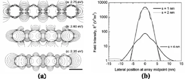
(45) directional flow of optical information. If the light can propagate unidirectionally and the scattering loss can be controlled, this plasmon light channel provides a potential application.. Figure 2.17: (a) Photograph of 20 nm diameter Au and Ag rods. The two labeled rods are typical of the ones used for these experiments. (b) Optical microscope image of a 4.7mm long Au rod exposed to through-prism TIR illumination at 532 nm. Note the strong scattering at the rod input and the absence of scattering at distal tip. (c) Image of the same Au rod under TIR illumination at 820 nm. Under these conditions, both ends of the rod exhibit strong emission/scattering. (d)-(e) A 4.7mm long Ag rod illuminated at 532 and 820 nm, respectively. Emission is observed from both tips at both wavelengths in the case of Ag. [15]. In theoretical analysis of plasmon propagation between metal nano-particles, L. A. Sweatlock shows a strong confine of electromagnetic wave between metal nanoparticles. Figure 2.18 illustrates the spatial images of the peak instantaneous electric field intensity at steady state for arrays of four 10-nm-diameter particles, excited on resonance. The distances between particle center are (a) 4 nm, (b) 2 nm, or (C) 1 nm. High confine electric energy is observed between particles. The maximum 23.
(46) local field occurs in the dielectric gap between the two metal particles at the midpoint of the array. For comparison, the maximum field intensity enhancement near an isolated nanoparticle driven resonantly is typically 30. The giant 5000-fold intensity enhancement is consistent with previous reports of the enhancement of the effective Raman scattering cross section near metallic nanostructures. Since this high confine and high enhancement of electric field energy, the light can be propagate in a metal nano-particles chain.. Figure 2.18: Two-dimensional spatial images of the electric field intensity in a plane through the particle centers of four Ag nanospheres with interparticles spacing of (a) 4 nm, (b) 2 nm, and (c) 1 nm at resonant excitation. [16]. They also show that there are two kinds of longitudinal resonance appeared in the particle chain. In Figure 2.19, the longitudinal component (Ex) of the electric field in a system which consists of a linear array of 12 touching Ag spheres excited at the two resonance frequencies. Areas colored red have positive field amplitude, where areas colored blue have negative field amplitude. In a snapshot of the chain driven by a longitudinally polarized plane wave at 0.35 eV (panel (a)), regions of positive Ex are observed at either end, with negative Ex throughout the particle array. This electric field pattern indicates that positive surface charge is concentrated on the rightmost. 24.
(47) particle and negative charge on the leftmost particle. The mode is typical of a single-wire antenna and requires surface charge to flow from particle to particle along the entire length of the array. Alternatively, when the same structure is driven at 1.65 eV (panel (b)) the coupled-dipole resonance is selectively excited. The field diagram alternates from positive in each dielectric gap to negative inside each particle. This indicates an alternating surface-charge distribution in which each individual particle is polarized but electrically neutral.. Figure 2.19: Distribution of the longitudinal component of the electric field in the vicinity of an array of 12 Ag particles with 10 nm diameter, illustrating two distinct modes. In panel (a), an antennalike mode resembling that of a single elongated wire is excited resonantly at 0.35 eV; in panel (b), a coupled-particle-like mode resembling that of a chain of independent particles is excited resonantly at 1.65 eV. The slight axial asymmetry of the filed distribution is caused by superposition of the resonant mode with the exciting plane wave. [16]. Due to the great utility of wavelength tunability and localfield enhancement for applications such as nonlinear optics and sensing of small volumes, nanosized ordered or quasiordered ensembles of very closely spaced metal particles serve as an ideal platform for active device regions in integrated plasmonic networks. Innovative nanoscale engineering and fabrication ssuch as the ion irradiation technique used hered are required to synthesize particle arrays with these interesting properties.. 25.
(48) 2.3.4 Nanodot coupler with a surface plasmon polariton condenser On the base of the surface plasmons coupling and plasmon interference between nanoparticles array, which have been mentioned in above section, a more complex optical system can be constructed followed this idea. In order to increase the efficiency of exciting localized surface plasmon in the nanodot coupler than that excited by propagating far-field light, Wataru Nomura propose a surface plasmon polariton condenser for efficient far/near-field conversion. Figure 2.20 (a) shows the proposed optical far/near-field conversion device. The nanodot coupler consisted of a linear array of nanoparticles with diameters of 230 nm and they are separated by 70 nm. The condenser consisted of twelve scatterers with a diameter of 350 nm, aligned on an arc with a diameter of 10 µm. Incoming far-field light is first transformed into the two-dimensional SPP mode on the gold film. Then, the SPP is scattered and focused by the condenser as shown in Figure 2.20 (b) and (c). The plasmons condenser consists of several hemispherical metallic submicron particles, arranged in an arc structure. The input terminal of the nanodot coupler is located at the focal point. Finally, after the localized surface plasmon transmits through the nanodot coupler, it is converted into an optical near-field. FIB is use to fabricate the nanodot coupler and condenser and a silicon-on-insulator wafer is employed to avoid ion beam drift.. 26.
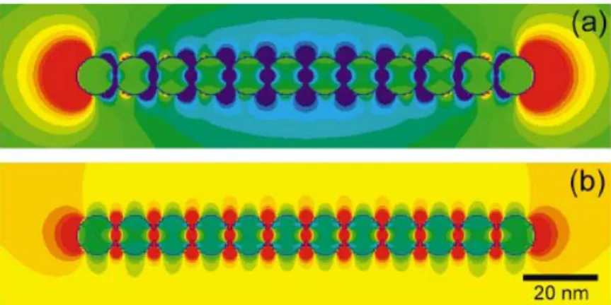
(49) Figure 2.20: Bird’s eye view of a nanodot coupler with a SPP condenser. (b) Experimental system. (c) Schematic illustration of the SPP condenser. [18]. In Figures 2.21(A), diagram (d) and (e) shows scanning electron microscopic (SEM) images of the condenser and nanodot coupler. Two barriers are fabricated in order to avoid illumination of the nanodot coupler by the higher-order diffraction [Fig. 2(d)]. Figures 2.21 (B), (a) and (b) show a shear-force image of the plasmons condenser and the spatial distribution of the optical near-field energy, respectively. We can find an efficient scattering and resultant focusing of the SPP by exciting the SPP mode through the grating coupler. In addition, Figure 2.21 (B), diagram (c) shows the spatial distribution of the optical near-field energy in the condenser calculated using the FDTD method. In the consideration of the tip diameter of 50 nm of the metallized fiber probe used for collection mode, the observed distribution, in diagram (b) and dashed curve in diagram (d), was in good agreement with the calculated results shown in diagram (d). Diagram (d) also shown the spatial distribution of the SPP was as narrow as 400 nm. These results imply that the device works as an efficient phased array.. 27.
數據
+7
Outline
Organization
Dielectric effect on localized surface plasmons
Future Development of LSPR
Preparation of silver nanoparticles film
Real time observation on the evolution silver nanoparticles film
Deposition of nano thick gold film
Diffraction property of gold nanoparticles gratings
Optical birefringence
Diffraction pattern and diffraction efficiency
Fabrication of CLC grating with Ag nanoparticles
相關文件
You are given the wavelength and total energy of a light pulse and asked to find the number of photons it
Reading Task 6: Genre Structure and Language Features. • Now let’s look at how language features (e.g. sentence patterns) are connected to the structure
Wang, Solving pseudomonotone variational inequalities and pseudocon- vex optimization problems using the projection neural network, IEEE Transactions on Neural Networks 17
volume suppressed mass: (TeV) 2 /M P ∼ 10 −4 eV → mm range can be experimentally tested for any number of extra dimensions - Light U(1) gauge bosons: no derivative couplings. =>
Define instead the imaginary.. potential, magnetic field, lattice…) Dirac-BdG Hamiltonian:. with small, and matrix
incapable to extract any quantities from QCD, nor to tackle the most interesting physics, namely, the spontaneously chiral symmetry breaking and the color confinement..
• Formation of massive primordial stars as origin of objects in the early universe. • Supernova explosions might be visible to the most
Monopolies in synchronous distributed systems (Peleg 1998; Peleg
