銅導線中電遷移效應所引發之故障特性探討
172
0
0
全文
(2) 銅導線中電遷移效應所引發之故障特性探討. An Investigation into the Characteristics of Electromigration Failure Mechanisms in Copper Interconnects 研 究 生:林明賢. Student:Ming-Hsien Lin. 指導教授:汪大暉 博士. Advisor:Dr. Tahui Wang. 國 立 交 通 大 學 電 子 工 程 學 系 電 子 研 究 所 博 士 班 博 士 論 文 A Dissertation Submitted to Department of Electronics Engineering & Institute of Electronics College of Electrical and Computer Engineering National Chiao Tung University in Partial Fulfillment of the Requirements for the Degree of Doctor of Philosophy In Electronics Engineering July 2006 Hsinchu, Taiwan, Republic of China. 中華民國九十五年七月.
(3) 銅導線中電遷移效應所引發之故障特性探討. 研究生: 林明賢. 指導教授: 汪大暉博士. 國立交通大學 電子工程學系 電子研究所 摘 要 隨著製程線寬快速縮小到奈米(sub-100nm)尺度時,後段連線系統中傳遞 的時間延遲(簡稱為 RC 延遲)已逐漸變成限制元件效能的主要因素。因此, 為了降低阻值和介電值,工業界已將金屬導線製程中所使用的材質,從鋁 (銅)/氧化層變成較低阻值的銅和較低介電係數的低介電材料。然而,銅導線 依舊需要解決電遷移所產生元件壽命失效機制的可靠度問題。快速地縮小銅 導線的寬度,同時又要維持高的電流承受能力,和更嚴格的可靠度標準需 求,電遷移效應將變成未來在銅製程中非常嚴峻的挑戰。 本篇論文將針對銅導線中電遷移效應所引發之故障機制的可靠性問題做 一系列的探討。第一章簡介電遷移的物理機制,第二章詳述實驗技巧和樣本 準備流程,第三章首先使用銅導線製程中不同的低介電值材料和不同的測試 結構互相比較其電遷移效應。不同的測試結構設計可以用來作故障模式分 析,進而找出連線系統中的弱連結,三層且兩端使用 via 作連結的金屬線發 現到電遷移壽命和所加的電流方向有很大的關係,再者,不同製程策略流程 會導致不同的電遷移結果及其故障模式。多重電遷移故障模式在銅雙鑲嵌式 製程中已被完整地研究。利用重疊和弱連結模型的統計方法可以決定每一個 故障模式的壽命,另外,根據阻值對時間變化關係圖,可以找出其對應的故 障模式的壽命。兩種方法得到非常一致的結果。. i.
(4) 接下來第四章,瞭解到連線系統中的弱連結,根據這資訊,一個很適合 研究銅導線和蓋層之間接面特性的電遷移結構被設計出來。藉著修改蓋層沉 積之前的清洗步驟和改變銅蓋層材料的方法,對電遷移壽命有相當顯著的改 善。吾人提出一個可能的機制來解釋這個電遷移壽命提高原因,並發現到蓋 層沉積前產生銅矽化合物(Cu-silicide)和銅/蓋層之間介面的黏著力對電遷移可 靠度有非常重要的影響,且銅/蓋層之間介面的黏著力可以直接關聯到其壽命 和活化能。 第五章接著研究電遷移在不同寬度從 0.12 到 10 微米和不同管洞/線 (via/line)的排列變化。線寬縮小對電遷移壽命變化有兩方面不同的現象,第 一是線寬小於 1 微米時,電遷移中位數故障時間(MTF)隨著線寬只有些微的 變化,除了因為 via 限制的條件。第二是線寬大於 1 微米時,在這區域 MTF 和線寬有著強烈的關聯。吾人提出一個可能的理論來解釋這個電遷移壽 命趨勢,對多晶結構的金屬線(寬度大於 1 微米),最主要擴散路徑是晶粒邊 界和表面擴散。對於線寬大於 1 微米時,主要的晶粒邊界擴散的活化能大約 比起表面和晶粒邊界擴散的活化能高 0.2 eV。使用在電遷移下銅移動速度, 亦可得到其相對的活化能,其結果與量測值相當一致。在銅連線系統中,控 制電遷移壽命的機制已被完整地研究,進而可以藉著巧妙設計 via 連線而達 到最常的壽命。 第六章,利用不同金屬線長度的結構,不同的電流密度和更接近真實情 況的三層結構,吾人對電遷移中的短線長度效應作一系列完整的研究,銅製 程已被良好的開發,確保缺陷不會造成影響。使用壽命量測和阻值劣化隨時 間變化的關係來描述這現象。吾人提出一個簡單的模型理論來解釋不同長度 和電流組合時的電遷移壽命趨勢,結果指出臨界長度值(jL)c 和溫度相關,在 250 和 300 度 C 區間隨著溫度下降而上升,藉著一系列電遷移實驗可以得到 非常多深刻的理解,更可層別出銅鑲嵌技術其電遷移的特殊行為。. ii.
(5) 最後於第七章,總結本論文的結論,並對未來研究方向提供一些建議。 此研究針對銅導線中電遷移效應所引發之故障機制的可靠性問題做一系列的 探討。從設計測試電遷移結構,找出銅鑲嵌製程在連線中最弱的部分,接 著,利用製程改變找出提高銅電遷壽命的方法,並提出模型解釋。最後,改 變銅導線的幾何寬度、長度和不同 via/line 結構作一系列研究,實驗結果可由 吾人的理論解釋,並提供給設計者對於電遷移可靠度設計的規範。藉著這一 系列電遷移實驗可以得到非常多深刻的理解,更可層別出銅鑲嵌技術其電遷 移的特殊行為。 關鍵字 : 電遷移,銅連線,多重失效模式,銅矽化合物,附著力,銅/蓋層 介面,表面擴散,晶粒邊界擴散,短長度效應。. iii.
(6) An Investigation into the Characteristics of Electromigration Failure Mechanisms in Copper Interconnects Student: Ming-Hsien Lin. Advisor: Dr. Tahui Wang. Department of Electronics Engineering & Institute of Electronics National Chiao-Tung University. Abstract. The back-end-of-line (BEOL) RC delay has gradually become a major limiting factor in circuit performance as a result of the rapid shrinking of critical dimensions. With reduced resistivities and dielectric constants, the metallization system for the interconnect structures has shifted from Al(Cu)/oxide to copper/low-k dielectrics. However, Cu interconnects still pose a reliability concern due to electromigration-induced failure over time. The rapid decrease in Cu conductor dimensions while maintaining a high current capability and a high reliability has emerged as a serious challenge. The objective of this dissertation is to investigate the characteristics and failure mechanism involved in Cu electromigration. Chapter 1 gives an introduction to the topic and discusses the background to study. Chapter 2 describes electromigration testing and analysis techniques in detail, and is intended to help familiarize the reader with the experimental aspects of this work in order to create a basis of understanding for the results sections that follow. In Chapter 3, first of all, Cu interconnect electromigration is examined using three low-k materials (k= 2.65 ~ 3.6) in a variety of structures. A number of test structures were designed to identify the EM failure modes and the weak links in the interconnect system. A strong dependence on current direction in the electromigration lifetime of three-level via-terminated metal lines was shown. Moreover, individual processing approaches lead to distinct EM behaviors and related failure modes. Multimodality in the electromigration behavior of Cu dual-damascene. iv.
(7) interconnects was studied. Both superposition and weak-link models were used for the statistical determination of the lifetimes of each failure model (statistical method). Results correlated to the lifetimes of the respective failure models physically identified according to resistance time evolution behavior (physical method). A excellent agreement was achieved. Based on the above understanding, the weak links of interconnect system were identified. Chapter 4 describes the correlation between the electromigration lifetime and the Cu surface caplayer process. An especially suitable EM test structure was designed to evaluate the properties of the Cu cap-layer interface. A significant improvement in electromigration lifetime is achieved through modification of the pre-clean step before the deposition of the cap-layer and by changing the Cu cap/dielectric materials. A possible mechanism for the enhancement of EM lifetime was proposed. A Cu-silicide formation prior to cap-layer deposition and the adhesion of the Cu/cap interface were found to be the critical factors in controlling Cu electromigration reliability. The adhesion of the Cu/cap interface can be directly correlated to the electromigration MTF and the activation energy. Chapter 5 outlines the effects of width scaling and layout variation on dual-damascene Cu interconnect electromigration. Electromigration versus line width in the 0.12—10 µm range and the configuration of the via/line contact has been investigated. There are two scenarios that cover the impact of width scaling on electromigration. One is the width <1 µm region, in which the MTF shows a weak width dependence, except under the via-limited conditions. The other is the width >1 µm region, in which the MTF shows a strong width dependence. A theory was proposed to explain the observed behavior. For polycrystalline lines (width >1 µm), the dominant diffusion paths are a mixture of grain boundary and surface diffusion. The activation energy for the dominant grain boundary transport (width >1 µm) is approximately 0.2 eV higher than that of the surface and grain-boundary transport (width ~ 1 µm). The derived activation energies for both grain-boundary and surface diffusion are obtained from the Cu drift velocity under EM stressing. The activation energy data obtained from both the measured and derived methods for both the surface and grain-boundary transport were found to be compatible. The mechanisms governing. v.
(8) the EM lifetime of interconnects leads to the identification of via interconnect design rules for maximizing electromigration lifetime. In Chapter 6, the electromigration short-length effect is investigated through experiments on lines of various lengths (L), being stressed at a variety of current densities (j), and using a technologically realistic three-level structure. This investigation represents a complete study of the short-length effect following the development of an enhanced dual-damascene Cu process. Lifetime measurement and resistance degradation as a function of time were used to describe this phenomenon. A simplified equation is proposed to analyze the experimental data from various combinations of current density and line length at a certain temperature. The resulting threshold– length product (jL)C value appears to be temperature dependent, decreasing with an increase in temperature in a range of 250oC to 300oC. Finally, Chapter 7 summarizes the results of the study and outlines some potential future directions for research into the interconnect electromigration reliability field. The multimodality distributions in various Cu/low-k processes are fitted using various bimodal methods to obtain precise lifetime values. Methods of optimizing the Cu electromigration performance have been investigated through Cap/dielectric interface re-engineering. Geometric variations of the test structure, including width scaling, length scaling, and vai/line configuration effects, were investigated to reveal the characteristics of Cu electromigration. A possible model is proposed to explain the electromigration behavior, and provides the means to ensure future design-in reliability. Much insight into electromigration failure modes and characteristics has been gained through experimentation using Cu dual-damascene technology to identify its distinctive behaviors.. Keyword: Electromigration, Cu interconnects, Multimodality failure, Cu-silicide, Cu/cap interface, Adhesion, Surface diffusion, Grain boundary diffusion, Blech effect.. vi.
(9) Dedication. To my wife 瓊足. vii.
(10) Acknowledgments I am grateful to my supervisor, Prof. Tahui Wang for his guidance and support through the years at NCTU. I would like to thank all of the committee members for their invaluable comments and suggestions.. This research was supported by measurements and samples from UMC Reliability Engineering and Technology Development. The industrial collaboration has made this research possible. I gratefully acknowledge helpful discussions with Dr. Gwo-Shii Yang, Dr. Ming-Shi Yeh, Ms. Yealing Lin, and many colleagues on several points in this thesis.. During the freshman period in the Emerging Devices and Technology Lab, I got a lot of help from Dr. Min-Cheng Chen, Dr Jun-Wei Wu, Dr Shau-Hong Ku, and Mr. Chin-Chang Cheng, a special thanks are also given to them.. Most importantly, I am indebted to the support and encouragement I have received over the years from my parents and family. I would like to thank my parents-in-law, for their kindness to bring up my lovely daughters. I am grateful to my wife, Joanne Wang, for her love and dedication. Without her, the road to my doctoral degree would have been immeasurably more difficult and lonely.. viii.
(11) 謝 誌 終於到了要準備寫致謝辭階段,多少夜晚辦公室無人,只剩我仍在為論 文埋首思考,今天仍舊如此但是心情卻是喜悅。首先,這本博士論文的完 成,必須感謝我的指導老師汪大暉教授。在做學問上,他有深厚的理論基礎 及嚴謹的態度,再加上細心與耐心的指導態度,使我能完成本論文。 特別感謝本論文口試委員們,所給予寶貴的建議與指教。 感謝聯華電子可靠度部門的協助及研發部門提供晶片測試。在論文的研 究上必須感謝許多曾經幫助予指導過我的許多長官 , 同事 , 學長,及學弟。 首先感謝楊國璽博士、葉名世博士、林雅玲在工作上的互相支持與指導、及 古紹泓,陳旻政博士在我剛進研究生活的指導與鼓勵。 感謝我的岳父母,在攻讀博士班其間幫助我照顧兩個可愛的女兒,有他 們在背後無怨無悔的付出與關心,讓我毫無顧忌的專注於論文研究,使得這 本博士論文得以順利完成。感謝我母親支持,很遺憾父親無法參加畢業典 禮,謹將這論文獻給他。 在此,謹將這份榮耀獻給我最摯愛的妻子和女兒。. ix.
(12) CONTENTS Chinese Abstract. i. English Abstract. iv. Acknowledgements. viii. Contents. x. Table Captions. xiii. Figure Captions. xv. List of Symbols. xxiii. Chapter 1. Chapter 2. Introduction. 1. 1.1. Interconnect Reliability. 2. 1.2. Basic Electromigration Physics. 3. 1.2.1 Diffusion and Atom movement is a solid. 3. 1.2.2 Electromigration Phenomenon. 6. 1.2.3 Theory of Electromigration. 6. 1.2.4 Effect of stress on electromigration. 8. 1.3. Electromigration Lifetime Model. 9. 1.4. Thesis Statement. 11. 1.4. Organization of Thesis. 11. Experimental Techniques. 20. 2.1. Interconnect Processing. 20. 2.2. Sample Package. 21. 2.3. Electromigration Testing. 22. x.
(13) Chapter 3. Copper Interconnect Electromigration Behavior in Various Structures and Precise Bimodal Fitting. 30. 3.1. Preface. 30. 3.2. Experimental Detail. 31. 3.3. Results and Discussion. 32. 3.3.1 EM performance of various structures and weak link of interconnect system 3.3.1.1 Pure metal line EM performance and width effect. 32 33. 3.3.1.2 Stress current direction and failure mode in various viaterminated structures. 3.4. Chapter 4. 34. 3.3.1.3. Weak link of copper interconnect system. 37. 3.3.2 Practical method of bimodal fitting. 38. Summary. 40. Copper Interconnect Electromigration Lifetime Improvement through Cap/dielectric Interface Reengineering. 59. 4.1. Preface. 59. 4.2. Experimental Detail. 60. 4.3. Results and Discussion. 61. 4.3.1 The effect of geometrical layout on MTF. 61. 4.3.2 The effect of pre-treatment on MTF. 63. 4.3.3 The effect of cap-layer material on MTF. 66. Summary. 67. 4.4. Chapter 5. Effects of Width Scaling and Layout Variation on Dual Damascene Copper Interconnect Electromigration. 79. 5.1. 79. Preface xi.
(14) 5.2. Experimental Detail. 80. 5.3. Results and Discussion. 81. 5.3.1 The via/line configurations on EM performance. 81. 5.3.2 The microstructure grain size of Cu.. 82. 5.3.3 The behavior of EM MTF on Wide Line Regions. 83. 5.3.4 The Theory of Drift Velocity on Wide Line Region. 85. Summary. 88. 5.4. Chapter 6. Blech Effect on Dual-Damascene Copper Interconnect. 103. 6.1. Preface. 103. 6.2. Experimental Detail. 105. 6.3. Results and Discussion. 106. 6.3.1 The short length effect on TTF distribution. 106. 6.3.2 The Length scaling effect on n value. 108. 6.3.3 A model to determine the threshold-length. 109. 6.3.4 Temperature dependence on Blech effect. 111. Summary. 112. 6.4. Chapter 7. Conclusions and Future Work. 125. 7.1. Summary and Conclusions. 125. 7.2. Future Work. 127. References. 131. Vita. 142. Publication Lists. 145. xii.
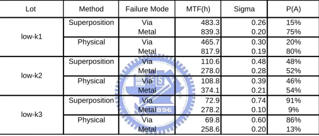
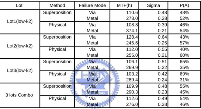
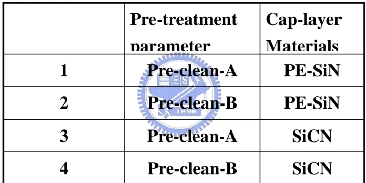
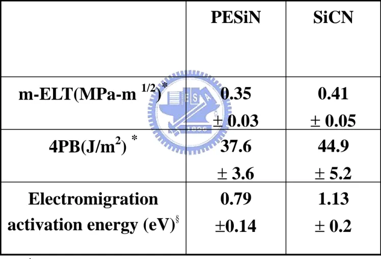
(15) TABLE CAPTIONS Chapter 2 Table 2.1. Illustrates EM oven temperature accuracy verification. Standard measured value is obtained from the calibrated thermocouple. The temperatures at four corner of the oven are measured to verify the thermal uniformity.. Chapter 3 Table 3.1. Summary of the five parameters [ P(A), MTF_A, σA, MTF_B, σB ] of superposition model extracted by iteration fitting (R2=0.991), the four parameters [ MTF_A, σA, MTF_B, σB ] of the weak link model extracted by iteration fitting (R2=0.987), and the fitting results of statistical methods with the data from the physical fitting method.. Table 3.2. Fitting results of statistical methods compared with those data from physical fitting method. The test structure consisted of a 0.2 µm wide, 400 µm long dual-damascene Cu M2 line. The low-k1, low-k2 and low-k3 are represented as SiOC, FSG and SOD, respectively. “Lot” means signifies a different batch of wafers using the same process flow.. Table 3.3. Key parameters of individual lot, combo lots using Cu/FSG materials obtained by both statistical and physical fitting methods. The test structure consists of a 0.2 µm wide, 400 µm long dual-damascene Cu M2 line.. Chapter 4 Table 4.1. The process split studied is summarized. The pre-clean A and pre-clean B represented various gas species and the gas flow used. The cap-layer SiCN was a nitrided form of SiC. Table 4.2. Comparison of adhesion and electromigration activation energy on different cap dielectric layer. SiCN shows better adhesion than PE-SiN for both measurement. xiii.
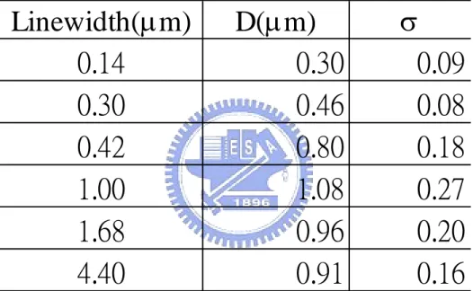
(16) methods. Pre-clean B was employed for adhesion test samples. Sample size is 8 x 40mm2 for 4PB, 10 x 10 mm2 for m-ELT, respectively.. Chapter 5 Table 5.1. Median grain size (probability=0.5) (D) and standard deviation (σ) versus metal line widths.. xiv.
(17) FIGURE CAPTIONS Chapter 1 Fig.1.1. Cross-section of Hierarchical Scaling in an Integrated Circuit showing multi-layer interconnects on top of a device. Source: the ITRS 2005 edition [1.1].. Fig.1.2. Demonstrates Delay for metal 1 and global wiring versus feature size. Source: the ITRS 2005 edition [1.1].. Fig.1.3. Interconnect reliability requirement versus total interconnect length in different years. FITs (1 failure in 109 hours of service =1 FIT), Source: the ITRS 2005 edition [1.1].. Fig.1.4. Simple representation of grains and grain boundary regions. This is a cross section of a columnar polycrystalline film with square grains. l is the grain width and length and d is the grain boundary width, l>>δ, Source [1.4].. Fig.1.5(a). Schematic representation of the motion of an atom and a vacancy in lattice diffusion [1.5]. Circles represent the atomic cores.. Fig.1.5(b) Schematic representation of the motion of an atom and a vacancy in grain boundary diffusion. Circles represent atom boundary, solid line is grain-boundary. Fig.1.6. Schematic representation of stress buildup due to depletion and accumulation of the metal atoms at the ends of the region. This stress causes a back flux of the metal atoms, which opposes the flux due to EM [1.4]. In bottom graph, the stress evolution during electromigration in a straight-line interconnect terminating block boundary.. Fig.1.7. Lifetime calculation from accelerated test need to be extrapolated to use conditions, which are typically at lower temperatures and current densities.. Chapter 2 Fig.2.1. A schematic summarizes the major aspects of dual-damascene process. (a) The trench and via is patterned in ILD layer. (b) The barrier and Cu seed are deposited. (c) Cu is electroplated to fill the via and trench. (d) Recess Cu film is removed using CMP process and cap-layer is deposited.. xv.
(18) Fig.2.2. (a) A top-down picture of 16-pin dual inline package. (b) Zoom-in the package, the wirebonds are used to connect to the bond posts of the package to the bond pads of the test structure.. Fig.2.3(a) The error percentage of 100 ohm precision resistor as the applied is 0.2mA for total devices under test (DUTs), and the error is smaller than 0.6%. Fig.2.3(b) The out resistance error percentage of 100 ohm precision resistor as the applied is 0.2mA for total devices under test (DUTs), and the error is smaller than 0.8%. Fig.2.4(a) Illustration the typical Joule heating calculation method. Reference line is obtained, as the current is relatively low. R(T) point is the measured resistance as stress high current. Joule heating temperature can be obtained from Tf minus oven temperature. Fig.2.4(b) Illustration the “two-current” typical Joule heating calculation method. Black solid line is actual temperature of metal line with zero applied current. Joule heating temperature is T minus oven temperature.. Chapter 3 Fig. 3.1. Schematics of EM test structures used: (a) NIST line. (b) via-terminated line, and (c) 30-via chain. The stress direction is defined by electron current flow direction.. Fig. 3.2. (a) MTF as function of line width for Cu single- and dual-damascene lines with J=10x106 A/cm2 at 300oC. Cu/SiOC low-k material is used. (b) TCR value as function of line width. Left: M1, right: M2.. Fig. 3.3. Typical time-to-failure distribution plots for upstream and downstream cases. The sample size is greater than 20 for upstream/downstream cases. Multimode was observed in the upstream, while a single log-normal function describes the typical downstream case. EM failure time were obtained at 300oC under a current density of 1.6x10⁶ A/cm2. The stress conditions are the same for all tests.. Fig. 3.4. Relative resistance vs. time degradation plots for (a) upstream case and (b) downstream case. Two different modes of degradation behavior are indicated in the upstream case, while only a long-lasting failure mode was found in the downstream case. Cu/FSG low-k material was used for this case.. xvi.
(19) Fig. 3.5. SEM image of representative upstream case (a) instantaneous failure (above); longlasting failure (below). (b) SEM image of representative downstream failure site.. Fig. 3.6. Log-normal time-to-failure distribution plots for upstream and downstream cases. EM failure time determined at 300oC under current density of 1.6x10⁶ A/cm2 for two cases. The upstream case shows much better EM performance than the downstream case. The sample size is 30/29 for the upstream/downstream cases. MTF=193.8 h, σ = 0.3 for upstream; MTF=24.6 h, σ = 0.74 for downstream case. The samples chosen for physical failure analysis were indicated. Data shown here are for Cu/FSG low-k material. Fig. 3.7. (a) In the upstream stress case, SEM images show trench depletion. Up-a and Up-b show different TTFs indicated in Fig. 6. (b) In the downstream stress case, SEM images show voids in the via/metal interface and trench depletion. D-c and D-d show different TTFs indicated in Fig. 6.. Fig. 3.8. (a) Cumulative lifetime of minimum allowable rule 30-via chains and single-via terminated metal lines in both stress directions. Data shown here are for Cu/SOD interconnect. (b) Left: 30-via chain resistance change vs. stress time. Right: IROBIRCH image indicates that the high resistance spot is located in the same stress current direction.. Fig. 3.9. (a) Lognormal time-to-failure distribution plots of two kinds of via chains with different line width arrangements. The sample size is 21/23 for Chain A/ Chain B. MTF=2.80 h, σ = 0.54 for Chain A, MTF=9.17 h, σ = 0.32 for Chain B. Stress conditions are the same for both splits. (b) SEM image of left: Chain A is M1/M2 (0.16 µm/3 µm); right: Chain B is M1/M2 (3 µm/0.20 µm). Cu/SOD low-k material was used.. Fig. 3.10 (a) Log-normal time-to-failure distribution plot using the superposition method (statistical method). A good fitting result was obtained after Levenberg-Marquardt iteration (R2=0.991). A poor fit curve shows initial guess result. (b) The same EM data was fitting by the weak-link method (statistical method). A good fit was obtained. xvii.
(20) (R2=0.987). A poor fit curve shows initial guess result. The EM failure time was obtained at 295oC under a current density of 1.28x10⁶ A/cm2 . Fig. 3.11 Bimodal fitting using the physical method. The physical method is defined according to relative resistance vs. time behaviors. Samples were manually grouped into two failure categories: instantaneous failure and long-lasting failure. Fig. 3.12 Many samples were analyzed by superposition (right) and physical (left) methods with bimodal fitting. The same stress conditions are used for all the samples. Fig. 3.13 The activation energy Ea extracted from via and line depletion modes. Fig. 3.14 Current density exponent n extracted from via and line depletion modes.. Chapter 4 Fig. 4.1. (a) Side view of via terminated line structure used in the present work. Stress direction is defined by electron current flow direction. (b) Top view of wide line with single via. The width of Metal =0.42 µm equals approximation 3x via diameter (0.14x0.14 µm2).. Fig. 4.2. (a) Illustrates relative resistance degradation vs. time plot. Left: wide line with 1 via. Right: wide line with 2 vias. (b) SEM image for two vias wide line structure, void was found in one via bottom, the other serves a current path.. Fig. 4.3. (a) Lognormal time-to-failure distribution plots for line end extensions of 0.06 vs. 0.0 µm. Cu/SiOC low-k material was used. (b) In this structure, the line-end between via and metal is zero. The via misaligning metal line may be due to process variation. The probability of misalign in no line-end extension is higher than that of the line-end extension.. Fig. 4.4. (a) Lognormal Time-To-Failure distribution plots for PE-SiN+pre-clean A and PESiN+pre-clean B. The sample size is 27/28 for PE-SIN+pre-cleanA/ PE-SIN+preclean B. MTF=77.8 hrs, σ = 0.58 for PE-SIN+pre-cleanA, MTF=24.4 hrs, σ = 0.56 for PE-SIN+pre-cleanB. Stress conditions are the same for both splits. (b) Relative resistance degradation vs. time plot for (i) PE-SiN+ pre-clean A.(ii) PE-SiN+ preclean B. The failure mode is almost same for both pre-clean recipes but the MTF is 3.2 times improvement for pre-clean A. xviii.
(21) Fig. 4.5. (a) Cu-wire initial resistance of PE-SiN and SiCN with pre-clean A or pre-clean B. The resistance of Cu wire with pre-clean A treatment is higher than that with preclean B for both cap-layer materials. The sample size is 30 for initial resistance extraction. The mean + standard deviation of resistance(%) is 127.1 + 2.1%, 119.4 + 2.6%, 119.6 + 3.1%, 107.5. + 3.9% for PE-SiN+Pre-clean A, PE-SiN+Pre-clean B,. SiCN+Pre-clean A, and SiCN+Pre-clean B, respectively. (b) Effect of different pre-clean treatment on TCR value. Fig. 4.6. High magnification TEM image on Cu/Cap interface. A very clear inter-layer with darker contrast between Cu and cap dielectric layer is observed and its thickness is about 80A.. Fig. 4.7. MTF (circles) and initial Cu wire resistance (squares) as a function of different split conditions. Error bars in MTF are the uncertainties to 90% CL. The split condition means that increase SiH4 gas prior to cap layer deposition. Relative reactive Si species concentration is indicated by arrow direction.. Fig. 4.8. (a) Schematic process flow of the Cu-silicide formation is shown. (b) Schematic process flow of the Cu-Nitridation reaction is proposed.. Fig. 4.9. Lognormal Time-To-Failure distribution plots for PE-SiN+ pre-clean B and SiCN+pre-clean A, The sample size is 27/26 for PE-SIN+pre-cleanB/ SiCN+pre-clean A. MTF=24.4 hrs, σ = 0.56 for PE-SIN+pre-cleanB, MTF=281.6 hrs, σ = 0.47 for SICN+pre-cleanA. Stress conditions are the same for both splits. Significant improvement of EM lifetime performance is achieved.. Chapter 5 Fig. 5.1. Schematics of EM test structures used (a). Via terminated line structure. Line length is equal to 400 µm. (b). Various EM structures for width dependence, left w=0.14 µm, middle w=0.42 µm, right w>0.42 µm. Stress direction is defined by electron current flow direction. Downstream is evaluated.. xix.
(22) Fig. 5.2. Typical Time-To-Failure distribution plots for Up-stream and Down-stream cases. The sample size is more than 24 for up-stream/down-stream case. EM fail time obtained at 300oC under current density of 1.6 ×10⁶ A/cm2. The worse case is downstream direction.. Fig. 5.3. Lognormal time-to-failure distribution plots for w=0.14, 0.3, 0.42 µm for downstream case. Similar distributions are shown. Stress conditions are the same for all tests.. Fig. 5.4. (a). Plot of the MTF as a function of linewidth (w< 0.42 µm), 90% confidence levels are lower and upper bound. (b). Plot of the MTF of different via/line configurations for 0.14 and 0.42 µm, stress conditions are the same for various structures.. Fig. 5.5. (a). FIB images of 0.14 µm(top), 0.42 µm(middle) and 1.0 µm(bottom) EM structures, bamboo like and mixture microstructure are shown. (b). Grain size distribution versus line widths.. Fig. 5.6. Lognormal time-to-failure distribution plots for w=1, 1.68, 2.1 and 3.5 µm for downstream case. Similar distributions are shown. Stress conditions are the same.. Fig. 5.7. SEM images for w=1.68 µm wide line structure. Void was found in via bottom. Large trench void cross other via is depleted. The bottoms of the vias are exposed. (a)-(c) represent different failure samples.. Fig. 5.8. Plot of TCR as a function of line widths. It reaches a maximum at w ~ 1 µm and then slightly decreases to a constant value.. Fig. 5.9. Plot of the MTF as a function of line widths. 90% confidence levels are lower and upper bounds. For w>0.42 µm, sufficient vias are designed to relieve the via-limited issue. Stress conditions are the same.. Fig. 5.10 The activation energy Ea as a function of line widths. Fig. 5.11 Plot of mean Cu drift velocity under EM stressing as function of line widths and sample temperatures. The solid lines are least-square fitting. Fig. 5.12 Plot of ZS*δSDSρj and ZGB*δGBDGBρj as function of 1/kT. The solid lines are leastsquare fitting.. xx.
(23) Chapter 6 Fig. 6.1. Schematic diagram of the 0.14 µm wide three-level via terminated line structure. The stripe length L is 5, 10, 25, 50, 100, 200, or 400 µm. Stress direction is defined by electron current flow direction. Down-stream is evaluated in this study.. Fig. 6.2. Log-normal time-to-failure distribution plots for L=50, 200, and 400 µm for downstream case. Similar distributions are shown for 200 and 400 µm, but wider distribution was found for L=50 µm. EM fail time obtained at 300oC under current density of 1.6 ×10⁶ A/cm2.. Fig. 6.3. The sigma of log-normal distribution vs. jL2. Smaller jL2 values shows large TTF dispersion. The solid curve is plotted using the statistical distribution of the critical void volume.. Fig. 6.4. Relative R change vs. time plots for L=25, 50, 100 and 200 µm. Different resistance onset times are shown for various line lengths. Stress conditions are the same.. Fig. 6.5. Log-log plot of MTF vs. current density-length product for L=50, 400 µm at 300 oC. The solid line was obtained by fitting the MTF data into Eq. 6.5, where the regression found (jCL)=6000 A/cm and n2=1.2. The dashed lines indicate n=1.4, 1.36 which fitting the MTF data of L=50, 400 µm to Eq. 6.4 and assuming that the exponential term is constant, a linear regression yields a current exponent of n1≈1.4, 1.36 respectively at high current density-length product.. Fig. 6.6. (a) L/MTF versus current density-length product for L=50 µm. The threshold–length products (jL)C was calculated to be 6319 A/cm for 300oC. (b) L/MTF versus current density-length product for L=25 µm. The threshold–length products (jL)C was calculated to be 4314 A/cm for 300 oC. Error bars represent 90% confidence intervals.. Fig. 6.7. (a) Relative R change vs. time shows slight resistance increase up to 5100 hrs of testing for L=25 µm, j=1.6 ×10⁶/cm2, T=300 oC, and sample size over 24. The resistance change is very small around 2 to 4%, show that the immortal behavior occurs, (jL)C»4000 A/cm. (b) Relative R change vs. time shows slight resistance. xxi.
(24) increase up to 5100 hrs of testing for L=10 µm, j=1.6 ×10⁶/cm2, T=300 oC, and sample size over 24. (jL)C »1600 A/cm. Fig. 6.8. (a) SEM images for L=10 µm line structure after passage of 1.6 ×10⁶/cm2 for about 5100 h at 300 oC. No clear void was found at the anode or cathode ends along the line. (b) A high-resolution TEM was analyzed at the cathode end to reveal the detail microstructure. Very small void has formed at cathode end, which lead to an only minor resistance increase. Fig. 6.9. FIB and TEM images of a stripe 5 µm length after passage of 1.6 ×10⁶/cm2 for about 5000 h at 300 oC. The EM-induced void of a stripe 5 µm length is much smaller than that of 10 µm length.. Fig. 6.10 An example of FIB cross sections at the cathode end along the 25 µm length line after passage of 1.6 ×10⁶/cm2 for about 5000 h at 300 oC. The void has partially exposed the bottom of the via. Fig. 6.11 Temperature dependence of critical length effect and maximum stress difference in the interconnect for L=25, 50 µm. It is observed that jL value increase slowly at low temperature.. Chapter 7 Fig. 7.1. A schematic AC pulse current, the current is applied every P period and remains on for a time ton, so that the duty cycle r = ton/P.. Fig. 7.2. Pulse DC waveform as ton =1ms, which is extracted from the scope.. xxii.
(25) LIST OF SYMBOLS A. material constant based on the microstructure and geometric properties of the conductor. B. Effectice elastic modulus. C. Concentration of atoms (atoms/cm3). CDF. Cumulative density function. d. Grain size. D. Diffusion coefficient. D0. Diffusion coefficient at the limit of an infinitely high temperature. Dgb. Diffusion coefficient along the grain boundary. DI. Diffusion coefficient through the interface. Dl. Diffusion coefficient through the lattice. Dp. Diffusion coefficient through the pipe. Ds. Diffusion coefficient through the surface. Deff. Effective Diffusion coefficient. e. The fundamental electron charge. E. Electric field. Ea. Activation energy. fgb. The fraction of atoms diffusing along the grain boundary. fl. The fraction of atoms diffusing through the lattice. j. Current density. Ja. The atomic flux. Jgb. The atomic flux along grain boundary. Jl. The atomic flux along lattice. (jL)C. Threshold–length product. k. Boltzmann constant xxiii.
(26) l. The columnar grain length. L. Metal length. MTF. Median time to fail. n. Current density exponent. P(A). Probability of one failure mode A. R. Resistance. T. Temperature (in K). T50. the 50th percentile fail time of a failure population. TTF. Time to fail. TCR. Temperature coefficient of resistance. Vfail. Failure volume. vd. Drift velocity of Cu. w. Metal width. Ze. Electrostatic charge. Zw. Electron wind charge. Z*. Effective charge. σ. Deviation in time to failure. σs. Stress in the metal line. δ. Grain boundary thickness. δGB. Width of grain boundary. δI. Width of metal/liner interface. δS. Width of surface. µ. Mobility. ρ. Electrical resistivity. Ω. Atomic volume. xxiv.
(27) Chapter 1 Introduction. Beginning in 2000, Integrated Circuit (IC) technology has been driven towards the nanotechnology era in the pursuit of higher performance and integration. It has become increasingly desirable to integrate greater functionality in a single chip. However, interconnecting the devices using metal wires consequently occupies a larger percentage of the available space. In addition to achieving a higher density, smaller devices and a larger number of metal layers are required. ICs can have up to 11 metal layers, as used in 65nm designs, for programmable logic devices. Figure 1.1 shows the cross-section of hierarchical scaling in an integrated circuit. According to the International Technology Roadmap for Semiconductors (ITRS), 2005 edition [1.1], 1212 meters of interconnect length per centimeter squared of active area will be required to construct a high-performance chip in 2006. For a million-transistor microprocessor chip, an average interconnect length of ~ 100 µm is suggested, but actually a distribution of both shorter and longer lines is present. Critical interconnects such as clock, control, and data lines between processor and cache may run the entire length of a chip and be 1-2 cm long. Interconnect delay related to resistance (R) and capacitance (C) has become the more dominant concern rather than over gate delay issues that were the primary focus prior the ULSI era, as shown in Fig. 1.2. The parasitic effects introduced by the metal line display a scaling behavior that differs from the active components such as transistors, and they tend to gain in importance as device dimensions are reduced and circuit speed is increased. In fact, they start to dominate some of the relevant metrics of digital IC such as speed, energy consumption, and reliability. A careful and in-depth analysis of the role and behavior of the interconnect metal line in semiconductor technology is, therefore, not only desirable, but also essential.. 1.
(28) 1.1 Interconnect Reliability The increasing complexity and performance of semiconductor products in combination with continuous feature size scaling imposes many new reliability challenges. For upcoming technology nodes, the introduction of new materials, processes, devices and packaging techniques will require the investigation of many additional advanced reliability engineering methods. IC reliability involves many disciplines, such as design, processing, assembly, and testing. Typically, manufacturers design an IC to have an operating lifetime of 10 years. Product reliability is assured if each of the elements contained in the product is reliable for that length of time. Product reliability consists of three major elements: design reliability, process reliability, and assembly reliability. If the reliability of each element matches the required lifetime, then product reliability is assured. ICs are composed of a large number of discrete components, such as transistors, resistors, interconnects, dielectric thin film, and capacitors. These components are combined through process integration to produce ICs. One way to evaluate the reliability of the entire IC process is to measure the reliability of each of the major process modules. Some of the key modules from a reliability point of view are: (1) gate dielectric, (2) transistor, and (3) interconnects. In the nanotechnology era, the concept of design for reliability is extremely important. Reliability must be considered at all stages of IC development, including design, process development, and manufacturing. For example, the factor that limits IC Back-End-Of-Line (BEOL) reliability will change from total line length to the number of vias, via density and redundancy. Tools developed to cater for the concept can identify weak critical area and mitigate them automatically during the design process. From the interconnect design perspective, reliability is the quality by which the interconnects maintain signal integrity and produce the desired functionality over the lifetime of the chip. That is, the change of resistance in a metal interconnection, either as a series of vias or a 2.
(29) single metal line, must remain within the tolerance of the design rules as the current passes through it. It only takes the failure of one of these metal line segments or vias to cause the entire chip to fail. Consequently, interconnect reliability requirements have become more stringent, as shown in Fig. 1.3, and the issue will become a more critical challenge in the future. Electromigration has always been one of the primary interconnect reliability concerns, and investigation into the phenomenon has persisted to the present day, where it still remains a troublesome reliability issue, as reflected by the many publications and conference sessions devoted to the topic each year.. 1.2 Basic Electromigration Physics Assuming a thin Cu film line 0.1 µm wide and 0.2 µm thick carrying a current of 1 mA, the current density will be 5 x 10⁶ A/cm2. Such a high current density will cause mass transport in the line at a device operation temperature of 100oC. Mass transport resulting from the passage of a DC current has been identified as the cause of the majority of failures in the metal interconnect system of IC chips. This phenomenon, known as electromigration, demonstrates the atomic motion in a metal line under the influence of a supplied electric field, and is basically a diffusion phenomenon under a driving force. The electromigration phenomenon has been observed for more than a century [1.2]; however, it was first identified as a reliability problem in integrated circuit metallizations around 40 years ago [1.3]. Diffusion and atom movement in a solid, and a brief history and overview of electromigration theory will be given in this section.. 1.2.1. Diffusion and Atom movement in a Solid. Diffusion. is. defined as. the migration. of. atoms. under. the. influence. of. a. concentration-gradient driving force. Fick’s law, the phenomenological equation that defines diffusion, is written as: 3.
(30) Jm=-D. dC dx. (1.1). Concentration gradients (. dC ) in the positive x direction cause the transport of a mass flux of dx. atoms (Jm) in the negative x direction. If more atoms leave a region than enter it, in time, this loss of matter (. dC <0) leads to mass depletion, or even voids that can affect reliability. Such effects dx. may occur at the interface between different phases, the grain boundary, or through structural defects. The diffusion coefficient D, a measure of the extent of mass transport, depends on a number of factors, including the nature of the diffusing atoms, the specific transport path (i.e., lattice, grain boundary, dislocation, surface, etc.), temperature, and the concentration of the diffusing species. The temperature dependence of the diffusion coefficient D, the most important factor, is given by the equation: D=D0exp(-. Ea ) kT. (1.2). Where D0 is the diffusion coefficient at the limit of an infinitely high temperature, Ea is the activation energy, which is a characteristic of the diffusion paths in the given metal. There are many paths an atom can take during diffusion in a metal line. Because most interconnect materials are polycrystalline, modeling the diffusion in polycrystalline materials is necessary and fundamental. The key to understanding diffusion in polycrystalline materials is the presence of grain boundaries and the fast diffusion paths that they provide. The diffusion coefficients for the grain boundary and the lattice are different. In addition, the atoms can move between the two regions depending on their local concentration and segregation coefficient. The flux equations for any species in each path are simply [1.4]:. ∂C ) gb ∂x ∂C Jl=-Dl ( )l ∂x Jgb=-Dgb (. (1.3) (1.4). Where Dgb refers to the diffusivity along the grain boundary, and DL is the diffusivity through the 4.
(31) lattice. The simplest model assumes that there is an effective diffusion coefficient for a species that describes the net diffusion through a polycrystalline material. This Deff is just the sum of the diffusion coefficients in each of the two region types, grain boundary and lattice, each scaled using the relative cross-section area of each region. The larger the relative cross-sectional area of the region, the more atoms transport through that region, and the more weight is given to the diffusion coefficient of that region. The effective diffusion coefficient in this model is: Deff=Dlfl+Dgbfgb. (1.5). Where fl and fgb are the fraction of atoms diffusing through a given pathway. For example, consider diffusion through a structure with square columnar grains of length l, and grain boundary thickness δ, as shown in Fig. 1.4. The cross-sectional area of each grain is l2 and the area of the grain boundary is lδ. The fraction of the atoms diffusing through the grain boundary is thus: fgb=. gb _ area lδ δ = 2 = grain _ area l l. (1.6). In the general form of the effective diffusion coefficient, a number of pathways, such as surface, interface, grain boundary, pipe, and lattice diffusion need to be considered. The various pathways can be expressed as [1.5]: Deff=Dlfl+Dgbfgb+ Dsfs+ Dpfp+ DIfI. (1.7). The subscripts identify the pathways of diffusion, where s≣surface, p≣pipe, and I≣interface. As electromigration can occur through these possible pathways, then the notion of pathways requires the identification of the fastest path that drives electromigration failure [1.6]. It is common to have more than one driving force acting on a solid. Electric fields, electric currents, mechanical stress, humidity gradients, and temperature gradients are examples of forces that serve to accelerate device failure.. 5.
(32) 1.2.2. Electromigration Phenomenon. Electromigration is a combination of thermal and electrical effects on mass motion. However, before describing the phenomenon, the origin of stress in metallization should be briefly introduced. The difference in thermal expansion between the metal and the dielectric material is rigidly bonded, and can cause mechanical stress in the lines. The stresses already exist as a result of the metal stack deposition and alloying processes. For Al, passivated by Si3N4 deposited at an elevated temperature, the metal contracts upon cooling more than the nitride. The tensile stress results when the actual lattice spacing is greater than the thermal equilibrium. The result, therefore, is tensile stress in the Al, and compression in the Si3N4. The driving force in conventional SiO2 based materials is the tensile stress. The magnitude of stress in the confined Al line has been reported to be in a range of up to approximately 600 MPa [1.7]. With such a high level of stress, even small irregularities may have great effect as the Al tries to relieve itself of this large tensile stress. Since the Al is confined, it cannot relieve the stress by plastic deformation. It is believed the major relaxation of stress occurs by the diffusional creep of the atom, which causes void formation and growth. Thus, voids are created and grown. Even in the absence of a current, it has been observed that the resistance of the metal interconnect will degrade as a result of mechanical stress. This mechanism is called stressmigration (SM), and is one of the more unsettling reliability issues associated with metallization. The electromigration picture becomes even more complex if both a thermal and an electrical current are applied to the metal line.. 1.2.3. Theory of Electromigration. At a fundamental level, electromigration involves the interaction between current carriers and migrating atoms. It is generally accepted that in an electrical conductor, electrons streaming towards the anode can impart sufficient momentum to the atomic ion core to propel them into neighboring vacant sites. Figures 1.5(a) and (b) illustrate this atomic movement along the lattice 6.
(33) [1.8] and grain boundaries, respectively. The lattice diffusion is shown in Fig. 1.5(a), where circles represent atoms, and a cross at B represents a vacancy, or a missing atom. An elementary step in electromigration will occur when the atom at A is forced into the vacancy at B under the influence of electrons move from left to right. The atom must squeeze through at O between the atoms at M and N. The theory of “electron wind” accounted for the induced mass transport, an idea that laid the foundation for the basic understanding of electromigration. The concept of the “electron wind” driving force was first formulated by Huntington and Grone [1.9], who employed a semiclassical “ballistic” approach to treat the collision of the moving atom by the charge carriers and yielded a driving force depending on the type of defects and the atomic configuration of the jumping path. This mass transport resulting from the passage of a DC current can be the cause of failure in the metal interconnects system on an IC chip. When a high current passes through metals with high-atomic diffusivities, such as Al or Cu, the electrons can transfer some of their momentum to the metal atoms, causing them to move. Net atomic transport of metal ions arises under a supplied electric field as a result of two effects. The first of these effects is the interaction of the supplied electric field and the metal ions and is proportional to the product of the field strength E and the valence of the metal Z. The second effect is the momentum transferred to the ions from the electrons. This contribution is often referred to as the “electron wind” force. In Cu and Al, the “electron wind” force has been found to be about an order of magnitude greater than the electrostatic force [1.2]. The driving force is expressed usually in terms of an effective charge Z*, which includes the electrostatic (Ze) and the electron wind (Zw) contributions [1.2, 1.10]. The force on the atoms is found to be: Force=(Ze+Zw)eE ≡Z*eE =-Z*eρj. (1.8). where Z* is the effective ion valence or charge number [1.2,1.9], e is the fundamental electron charge, E is the electric field (E=ρj), ρ is the electrical resistivity of the metal, and j is the current density. As current density opposes the electron flow direction, a negative sign for j 7.
(34) results in a positive sign in Force. The atomic flux induced by the current (in the direction of the electron flow) equals the force times the mobility times the concentration and is thus: Ja=(Force)x(µ)x(C) =-Z*eρj µC=-. DC Z*eρj……………………………………(1.9) kT. where Ja denotes the flux of the atoms expressed in the number of atoms passing perpendicular to a reference surface of unit area in unit time (atoms per unit area per sec), µ is the mobility, C is the concentration of atoms (atoms/cm3), D is the diffusion coefficient, k is Boltzmann’s constant, T is temperature (in K), and the well-known Einstein equation is used. Equation 1.9 expresses the proportionality between atomic flux and electron flux. Ja is the atomic flux due to electromigration. Electromigration is thus characterized at a fundamental level by the material constants Z*, D, and ρ. Combining eq. 1.7 and 1.9, the various pathways for electromigration damage formation can be examined using Z*Deff term: * Dgbfgb+ Z s* Dsfs+ Z *p Dpfp+ Z I* DIfI Z*Deff = Z l* Dlfl+ Z gb. (1.10). Each pathway is anticipated to have a different Z* component because the “electron wind” force varies according to the local electronic environment surrounding a given atom.. 1.2.4. Effect of Stress on Electromigration. The atomic flux in eq. 1.9 is an oversimplification. In reality, as atoms move from one end of an interconnect to another under electromigration, a mechanical stress gradient is created in the line. This additional effect is a back flux of atoms that opposes the forward flux. This back flux is due to a stress gradient that occurs as a result of the depletion and build-up of metal atoms at the flux divergence points. Figure 1.6 illustrates this phenomenon [1.4]. When the metal atoms diffuse due to the “electron wind” force, they become depleted at the start of a polygranular cluster region and accumulate at the end of the region. The “electron wind” force creates tensile stress near the cathode where the atoms deplete, and compressive stress near the anode where the. 8.
(35) atoms accumulate [1.11]. The resulting stress gradient leads to mechanical driving force, referred to as the back-stress force, which opposes the “electron wind” force. The atomic flux can be described using the following equation [1.11]. Ja=-. ∂σ s DC (Z*eρj − Ω ) kT ∂x. where Ω is the atomic volume, and. (1.11). ∂σ s. ∂x. is the stress gradient along the line. The first. observations of the effect suggested that there is a critical line length below which the electromigration atomic flux can be entirely balanced by the stress-directed counter flux of atoms [1.12]. This is a steady-state condition, and the steady-state stress of eq. 1.11 is the stress that would be present at that time. If the metal, in its environment, can withstand this stress then failure will not occur. But if it cannot, then failure is likely. The stress at which failure occurs is called the critical stress, σcrit. Therefore, a criterion for the failure of an interconnect under elecromigration conditions could be if the steady-state stress is equal to or greater than a specific critical stress value.. 1.3 Electromigration Lifetime Model The reliability of a metal interconnect is most commonly determined by carrying out a lifetime experiment on a set of lines to obtain the median time to failure (MTF). The data for the actual time to failure for each line is plotted on a lognormal graph, and the value of T50 (the time at which 50% of the lines fail) is extracted, along with the lognormal shape parameter. In practice, the stress experiments are often based on tests conducted at accelerated conditions (i.e., high temperature and current densities), as shown in Fig. 1.7. If the failure mechanism is the same in both the accelerated and the standard operating conditions, the data is scaled back to design rule conditions (i.e., low temperature and current density). The lifetime extrapolation is commonly based on Black’s equation [1.13,1.14], which expresses MTF, or T50 (the 50th percentile fail time. 9.
(36) of a failure population), as:. 1 j. ⎛ Ea ⎞ ⎟ ⎝ kT ⎠. MTF= A( ) n exp⎜. (1.12). where A is a material constant based on the microstructure and geometric properties of the conductor, n is the current density exponent, j, Ea, and kT have previous definitions. In the electronics industry, the operating current density and temperature are the most important parameters in an interconnect system from a design perspective. The operating current density, juse or jmax, represents the maximum current density that the interconnect system can maintain while still guaranteeing a certain failure rate over a certain period of operation time at a standard operating temperature. To determine this value, a ratio of Black’s equation (eq. 1.12) between a standard operating and test conditions can be employed for extrapolation [1.15]:. TTFuse = MTFuse (. ⎡E juse − n 1 1 ⎤ ) exp ⎢ a ( )⎥ exp[ − Nσ ] − jtest ⎣ k Tuse Ttest ⎦. (1.13). where TTFuse is the time to failure under standard operating conditions, MTFtest is the median time to failure under accelerated test conditions, jtest is the test current density, Ttest is the test temperature, Tuse is the standard operating temperature, N is a constant that relates MTF to a time-to-failure at a different failure percentage, σ is the deviation in time to failure, and n, Ea and k have previous definitions. The expression term exp[-Nσ] in eq.1.13 relates the median time to failure to a different failure percent. An expression for juse can be written as eq.1.14 by rearranging eq.1.13.. juse. ⎡ ⎤ ⎢ ⎥ MTFtest 1 ⎢ ⎥ = jtest ⋅ ⎢ TTFuse ⎥ ⎡ Ea 1 1 ⎤ exp ⎢ ( )⎥ exp[ − Nσ ] ⎥ − ⎢ ⎢⎣ ⎥⎦ ⎣ k Tuse Ttest ⎦. 1. n. (1.14). where TTFuse is a known operating lifetime of 10 years or 105 hours for a given specification.. 10.
(37) 1.4 Thesis Statement The goal of this thesis is to investigate the characteristics and failure mechanisms involved in Cu electromigration. Cu interconnect test structures are characterized in terms of their design. The multimodality distributions in various Cu/low-k processes are fitted using various bimodal methods to obtain precise lifetime values. Methods of optimizing the Cu electromigration performance have been investigated through Cap/dielectric interface re-engineering. The dominant diffusion paths for polycrystalline lines (width >1 µm) are examined using activation energy extraction and a drift velocity model. The Blech effect on dual-damascene Cu interconnects is evaluated to reveal influence of the back-stress force on line length. Threshold–length product (jL)C values are determined using various methods. Much insight has been gained through electromigration experiments with Cu dual-damascene technology to identify its distinctive behaviors.. 1.5 Organization of Thesis This thesis consists of seven chapters. Chapter 1 gives an introduction to the topic and discusses the background to study. Chapter 2 describes electromigration testing and analysis techniques in detail, and is intended to help familiarize the reader with the experimental aspects of this work in order to create a basis of understanding for the results sections that follow. In Chapter 3, following the successful integration of Cu/low-k BEOL processes, package level electromigration tests have been performed using various low-k materials in order to compare the performance and verify the stability of the Cu dual-damascene process. Various stress conditions for a number of structures were studied enable an understanding of the failure modes and to identify the weak links in an interconnect system. In addition to a well-understood failure mechanism, a precise lifetime prediction methodology is essential in order to describe 11.
(38) circuit degradation due to electromigration damage. Chapter 4 describes the correlation between the electromigration lifetime and the Cu surface cap-layer process. An especially suitable EM test structure has been designed to evaluate the properties of Cu cap-layer interface. A three-level dual-damascene Cu interconnect line has been produced to allow a series of experiments to be carried out. This chapter illustrates the interface between the Cu line and the dielectric capping layer, pre-clean treatment prior to dielectric layer deposition. Chapter 5 outlines the effects of width scaling and layout variation on dual-damascene Cu interconnect electromigration. Electromigration experiments have been conducted using both wide and narrow lines in order to emphasize the main diffusion path in a full Cu dual-damascene process, since the electromigration diffusion mechanism may be different for both narrow lines and wide lines. A theory is proposed to explain the results. In Chapter 6, the Blech effect or the short-length effect on a dual-damascene Cu process and its temperature dependence is investigated by using a technologically realistic interconnect structure. The Blech effect is an important consideration from a reliability standpoint, since designers are able to create interconnect layouts that are mostly electromigration resistant by ensuring the majority of lines are below the critical length. In this work, an alternate means of determining the threshold–length product (jL)C value, and a model that relates it to the failure volume and atomic flux is proposed. A test was performed for a greatly extended time period to examine the extracted (jL)C values and verify the immortality of Cu/low-k interconnects. Finally, Chapter 7 summarizes the results of the study and outlines some potential future directions for research into the interconnect electromigration reliability field.. 12.
(39) Fig.1.1 Cross-section of Hierarchical Scaling in an Integrated Circuit showing multi-layer interconnects on top of a device. Source: the ITRS 2005 edition [1.1]. 13.
(40) 100 Gate Delay (Fan out 4 ). Relative Delay. Local (Scaled). Global with Repeaters. 10 Global w/o Repeaters. 1. 0.1 250. 180. 130. 90. 65. 45 32. Process Technology Node (nm). Fig.1.2 Demonstrates Delay for metal 1 and global wiring versus feature size. Source: the ITRS 2005 edition [1.1].. 14.
(41) (FITs/m length/cm2) x 10-3. 6 Year 2005. 5. 2006. 4. 2007. 3. 2008 2009 2010. 2 1 0 500. 1000. 1500. 2000. 2500. Total Interconnect Length (m/cm2). Fig.1.3 Interconnect reliability requirement versus total interconnect length in different years. FITs (1 failure in 109 hours of service =1 FIT), Source: the ITRS 2005 edition [1.1].. 15.
(42) Grain Interior. l. (lattice). Grain boundary. δ l. Fig.1.4. Simple representation of grains and grain boundary regions. This is a cross section of a columnar polycrystalline film with square grains. l is the grain width and length and d is the grain boundary width, l>>δ, Source [1.4].. 16.
(43) M. e-. o. B. A N. Fig.1.5(a). Schematic representation of the motion of an atom and a vacancy in lattice diffusion [1.5]. Circles represent the atomic cores.. e-. Fig.1.5(b). Schematic representation of the motion of an atom and a vacancy in grain boundary diffusion. Circles represent atom boundary, solid line is grain-boundary.. 17.
(44) eAtomic flux from EM. A. B. Cathode (–). Anode (+). Metal atom depletion. Back flux from stress. –tensile stress-. t1 t3. σss. 6.0E+02. Metal atom accumulation –compressive stress-. t2 t4. t1<t2<t3<t4. Tensile σ(stress). σ0. 0.0E+00. t∞. Compressive. -6.0E+02 0. Fig.1.6. 0.2. 0.4. Lp. 0.6. 0.8. 1. Schematic representation of stress buildup due to depletion and accumulation of the metal atoms at the ends of the region. This stress causes a back flux of the metal atoms, which opposes the flux due to EM [1.4]. In bottom graph, the stress evolution during electromigration in a straight-line interconnect terminating block boundary.. 18.
(45) Stress Condition. CDF(%). 50%. Use Condition. Extrapolate to use AF_temp*AF_current. top. 1e-1%. Fig.1.7. t50%(op). Product-based specification. Lifetime calculation from accelerated test need to be extrapolated to use conditions, which are typically at lower temperatures and current densities.. 19.
(46) Chapter 2 Experimental Techniques. In the following section, the experimental techniques used in this work will be described. This chapter is intended to help familiarize the reader with the experimental aspects of this work in order to create a basis of understanding for the following results sections.. 2.1 Interconnect Processing The fabrication of multi-level Cu interconnects is achieved using a dual-damascene process [2.1]. In a standard damascene process, the dielectric level is pattered first, then metal is deposited into the trenches, followed by chemical mechanical polishing (CMP) process to remove the excess surface layer and leave the material in the trenches. Figure 2.1 illustrates the process steps for Cu dual-damascene metallization. The first step is the deposition of a planar dielectric stack film, which is then patterned and etched using standard lithographic and dry-etch techniques to produce the desired via and wiring pattern. In order to protect the devices from damage by the diffusion of Cu, the vias and trenches formed in the dielectric layer must be coated with a diffusion barrier. This diffusion barrier material provides an efficient seal that prevent the Cu from migrating into the interlevel dielectric (ILD) and a surface on which the Cu seed can be deposited [2.2]. The barrier material used in this study was TaN/Ta, a bi-layer barrier in which a strong adhesion is formed between the TaN and the ILD, and is an excellent metal interface between the Ta and the Cu seed layer. The TaN/Ta liner and Cu seed layers were deposited sequentially using physical vapor deposition (PVD) [2.3]. In addition, resputtering results in excellent side wall coverage and void free vias. This seed layer provides a preferred surface to which Cu can be plated using an electrolysis method. The desired pattern is then filled with Cu. 20.
(47) using this electroplating process [2.4]. Once the trench or via is filled, the excess Cu must be removed using a chemical mechanical polishing (CMP) technique. Finally, a cap-layer is deposited to seal the top surface of the Cu film. The process is then repeated for each interconnect level.. 2.2 Sample package All electromigration testing conducted in this study was performed using package level testing. The wafers are first diced using a diamond saw to provide the dies that contain the electromigration test structures. These dies are then bounded on a 16-Pin dual inline package (DIP), as shown in Figure 2.2(a). The package consists of two rows of 8 pins that correspond to bonding posts that surround the well of the package. The wirebonds are used to connect the bond posts of the package to the bond pads of the test structure, as shown in Figure 2.2(b). The wirebonded packages are then loaded into the socket boards, which are then inserted into an electromigration testing oven. The current is applied to the electromigration test pattern through the socket boards to the package, and then through the wirebonds to the test structure. The main advantage of this technique is that it allows for the simultaneous testing of great numbers of samples. The drawbacks of package level testing are the high cost and time consumption. The wafer level technique is another electromigration testing method. In wafer level experiments, a wafer is placed on a hot-chuck, heated to the desired temperature, and then a probe card is lowered into contact with the test structure. An advantage of this method is that it does not require the expense of packaging the test structures. However, the technique is severely limited in that it can not effectively test a large number of samples simultaneously. Using the wafer level technique, it is difficult to maintain an adequate contact between the probe card and the test structure for testing period over hundred hours. In order to achieve a fast response (minutes to a few hours at most) from experimental testing, it is necessary to supply an extreme 21.
(48) high current on the test structure. A disadvantage of this rapid wafer level test is that large current densities that generate steep thermal gradients must be employed. Because of this, the measured lifetime may not physically extrapolate well to situations where a smaller current prevails. Consequently, the wafer level technique is not an industrial standard method for electromigration testing during the process qualification stage. On the contrary, the typical standard method for electromigration testing is at package level due to capability of measuring a large samples and using low stress current densities.. 2.3 Electromigration testing Electromigration testing is essentially the accelerated testing of interconnects using heat and electrical current as the accelerating factors. In this study, electromigration tests are conducted at temperatures in a range from 250oC to 350oC. The accuracy of the oven temperature can be guaranteed since the temperature setting is calibrated using standard thermocouple (K-type) procedure. The offset value between the set and the standard measured temperature, which is obtained from the thermocouple, is compensated by using a polynomial equation. Table 2.1 shows the minor deviations between the set and the standard measured temperature, and the offset equation can be written as: 0.00012344x2 + 0.99744059x + 0.17101501, where x is the standard measured temperature. The square of polynomial term is included to enable a higher accuracy. The temperatures at the four corners of the oven are measured to verify thermal uniformity. The specification of the oven is within a 3oC deviation. As in any accelerated testing, it is important to conduct the tests in a range of temperatures that allow for the same failure mechanisms that one might see at standard operating conditions (80 oC to 125 oC). The supplied current can also be used as an accelerating factor during electromigration testing. The accuracy of the supplied current is verified by measuring the precision resistors. The test was started after the temperature within the oven was stable. The current were turned on and 22.
(49) the resistance was monitored. Figure 2.2(a) shows the error percentage of a 100 ohm precision resistor at a supplied current of 0.2mA for each device under test (DUTs), and the margin of error is less than 0.6%. The accuracy of the current meter is within a 1% deviation of the specification and current source resolution is 10 µA. Figure 2.2(b) shows the out resistance error percentage of 100 ohm precision resistor as the applied is 0.2mA for each DUTs, and the error is less than 0.8%. Reduced stress current densities in the range of 0.6 to 2.0x10⁶ A/cm2 (defined with respect to the cross-section of the metal line) were used to limit any increase temperature due to Joule heating to a maximum of 3oC, even for low-k materials known to possess small thermal conductivity [2.5]. Higher current densities will induce local Joule heating that can occur at the site of defects, or in thinned Cu sections, during electromigration testing. The impact of this local Joule heating is difficult to characterize. However, this issue does not seriously affect the work being discussed in this study. Traditionally, Joule heating in electromigration testing has been quantified by measuring the metal line resistance at a relatively low current (i.e. the reference current), where the dissipated power and the related temperature increase were assumed to be negligible [2.6]. If the relationship is derived for the metal line resistance vs. temperature, the difference between the resistance measured at low current condition and the resistance measured under actual stress conditions (high current), respectively, can be easily translated into the actual metal line temperature under stress. Figure 2.4(a) illustrates the typical Joule heating calculation method. The Joule heating temperature can be obtained by subtracting the oven temperature from Tf. Unfortunately, the requirement of negligible Joule heating at low currents may result in significant resolution and noise related errors. In this work, the QualitauTM “two-current” method is used to extract the Joule heating value. The reference current can then be increased to a level where the corresponding accuracy is significantly improved. Measuring the resistance R(T) at several oven temperature values, using two selected current levels (one is stress current, the other 23.
(50) is reference current), enables the two related linear expressions to be established. If it is assumed that relationship between the R(T) and temperature is linear, a fitting line of the actual line temperature, in which the supplied current is extracted to zero, can be extrapolated. Figure 2.4(b) illustrates this “two-current” method, by which the actual temperature of metal line undergoing the electromigration test can be accurately determined. Electromigration testing in this work was performed using the QualitauTM semiconductor reliability testing system. The Mainframe contains the circuitry that stresses the DUTs, and the associated data acquisition electronics. DUTs are plugged into Zero Insertion Force (ZIF) sockets on printed circuit boards (DUT boards), which, in turn, are connected to the EM modules via cable assemblies. The oven temperatures can range up to 350oC with a N2 ambient. The power supply module delivers a fixed DC current with a total voltage compliance of about 9 volts in the range of currents used in this study.. 24.
(51) Dielectric Hard Mask CMP stop layer trench. (a). Low-k Cap layer. via. TaN/Ta, Cu seed. (b). Cu Plating. (c). Cap-layer Cu CMP. (d) Fig.2.1 A schematic summarizes the major aspects of dual-damascene process. (a) The trench and via is patterned in ILD layer. (b) The barrier and Cu seed are deposited. (c) Cu is electroplated to fill the via and trench. (d) Recess Cu film is removed using CMP process and cap-layer is deposited.. 25.
(52) (a). Wirebond. (b). Bond. Test structure Fig.2.2 (a) A top-down picture of 16-pin dual inline package. (b) Zoom-in the package, the wirebonds are used to connect to the bond posts of the package to the bond pads of the test structure.. 26.
(53) Current Error. 0.6% 0.4% 0.2% 0.0% -0.2% -0.4% -0.6% 0. 10. 20. 30. 40. 50. 60. No. of DUT Fig.2.3(a). The error percentage of 100 ohm precision resistor as the applied is 0.2mA. Out Resistance Error. for total devices under test (DUTs), and the error is smaller than 0.6%.. 0.8% 0.4% 0.0% -0.4% -0.8% 0. 10. 20. 30. 40. 50. 60. No. of DUT Fig.2.3(b). The out resistance error percentage of 100 ohm precision resistor as the applied is 0.2mA for total devices under test (DUTs), and the error is smaller than 0.8%.. 27.
(54) Line Resistance (ohm). 45. R(T) @Istress. 40 35. Reference Line (I is low). 30. Tf. 25 20 0. 100. 200. 300. 400. Oven Temperature (oC) Fig.2.4(a). Illustration the typical Joule heating calculation method. Reference line is obtained, as the current is relatively low. R(T) point is the measured resistance as stress high current. Joule heating temperature can be obtained from Tf. Line Resistance (ohm). minus oven temperature.. Stress Line (I is high). 50 45 40 35 30 25 20. R(T) @Istress Reference Line (I is low). Tf. 0. 100. 200. T. 300. 400. Oven Temperature (oC) Fig.2.4(b). Illustration the “two-current” typical Joule heating calculation method. Black solid line is actual temperature of metal line with zero applied current. Joule heating temperature is T minus oven temperature.. 28.
(55) Table.2.1. Illustrates EM oven temperature accuracy verification. Standard measured value is obtained from the calibrated thermocouple. The temperatures at four corner of the oven are measured to verify the thermal uniformity. 100℃. Oven Location. Thermal-couple Standard Sensor No. measurement. Right-up Right-down Left-up Left-down. B18436 B18430 B18438 B18428. Oven Location. Thermal-couple Standard Sensor No. measurement. Right-up Right-down Left-up Left-down. B18436 B18430 B18438 B18428. 100.8 100.6 100.3 99.9 250℃. 251.6 251.8 250.7 249.8. 150℃. Setting value. Standard measurement 100 100 100 100. Setting value. 150.4 150.7 149.9 149.6 300℃ Standard measurement. 250 250 250 250. 301.6 301.1 300.4 299.5. 200℃. Setting value. Standard measurement 150 150 150 150. Setting value. 200.6 201.0 200.1 199.1 350℃ Standard measurement. 300 300 300 300. 351.5 351.0 350.2 349.8. Fitting equation: 0.00012344x2 + 0.99744059x + 0.17101501, where x is the standard measurement temperature.. 29. Setting value 200 200 200 200. Setting value 350 350 350 350.
數據
![TABLE 3.1 Summary of the five parameters [ P(A), MTF_A, σ A , MTF_B, σ B ] of superposition model extracted by iteration fitting (R 2 =0.991), the four parameters [ MTF_A, σ A , MTF_B, σ B ] of the weak link model extracted by iteration fitting (R 2 =0](https://thumb-ap.123doks.com/thumbv2/9libinfo/8747360.205219/82.892.130.799.468.712/summary-parameters-superposition-extracted-iteration-parameters-extracted-iteration.webp)
+3
相關文件
When the spatial dimension is N = 2, we establish the De Giorgi type conjecture for the blow-up nonlinear elliptic system under suitable conditions at infinity on bound
• Many statistical procedures are based on sta- tistical models which specify under which conditions the data are generated.... – Consider a new model of automobile which is
Other advantages of our ProjPSO algorithm over current methods are (1) our experience is that the time required to generate the optimal design is gen- erally a lot faster than many
By correcting for the speed of individual test takers, it is possible to reveal systematic differences between the items in a test, which were modeled by item discrimination and
Although we have obtained the global and superlinear convergence properties of Algorithm 3.1 under mild conditions, this does not mean that Algorithm 3.1 is practi- cally efficient,
Courtesy: Ned Wright’s Cosmology Page Burles, Nolette & Turner, 1999?. Total Mass Density
•The running time depends on the input: an already sorted sequence is easier to sort. •Parameterize the running time by the size of the input, since short sequences are easier
• If we want analysis with amortized costs to show that in the worst cast the average cost per operation is small, the total amortized cost of a sequence of operations must be
