414 IEEE TRANSACTIONS ON ELECTRON DEVICES, VOL. ED-21, NO. 2, FEBRUARY 1980 Devices, vol. ED-19, no. 7, pp. 852-860, July 1972.
[8] M. G . Collet and L. J. M. Esser, “Charge transfer devices,” in Advances in Solid State Physics, H. J. Queisser, Ed. Stuttgart, Germany: Pergamon, pp. 337-357,1973.
[9] D. D. Buss, W. M. Bailey, and W. L. Eversole, “Noise in MOS bucket brigade devices,” IEEE Trans. Electron Devices, vol. ED- 22,110.11, pp. 977-981,Nov. 1975.
[ l o ] C. N. Berglund and K. K. Thornber, “A fundamental comparison of incomplete charge transfer in charge transfer devices,” Bell Syst. Tech. J., vol. 52, no. 2, pp. 147-182, Feb. 1973.
[11] D. B. Scott and S. G . Chamberlain, “A calibrated model for the subthreshold operation of a short channel MOSFET including surface states,” IEEE J. Solid-state Circuits, vol. SC-14, no. 3, pp. 633-644, June 1979.
[ 121 L. G. Heller and H. S. Lee, “Charge transfer device modeling,” in Semiconductor Silicon 1973, H. R. Huff and R. R. Burgess, Eds. Princeton, NJ: Electrochemical SOC.
[13] M. G. Buehler, “Dopant profiles determined from enhancement- mode MOSFET d.c. measurements,” Appl. Phys. Lett., vol. 31, pp. 848-850, Dec. 1977.
An Analysis and the Fabrication Technology of the
Lambda Bipolar Transistor
Abstract-A new type of voltage-controlled negative-differential- resistance device using the merged integrated circuit of an n-p-n (p-n-p) bipolar transistor and an n(p)-channel enhancement MOSFET, which is called the Lambda bipolar transistor, is studied both experimentally and theoretically. The principal operation of the Lambda bipolar tran- sistor is characterized by the simple circuit model and device physics. The important device properties such as the peak voltage, the peak cur- rent, the valley voltage, and the negative differential resistance, are derived in terms of the known device parameters. Comparisons be- tween the characteristics of the fabricated devices and the theoretical model are made, which show that the analysis is in good agreement with the observed device characteristics.
N
I. INTRODUCTION
EGATIVE-differential-resistance semiconductor devices have offered increasing interest in oscillator circuit and memory applications. So far, there are several realized struc- tures which had been proposed. Among these, Kano et
aZ. [ I ] reported a structure with two terminals called the Lambda diode, which consisted of two integrated comple-
mentary JFET’s. Several important applications of the Lambda diode had also been proposed [2] -[6]. Baliga et al. [7], [8]
reported an integrated structure with three terminals called the GAMBIT which consisted of the merged structure of a p-n-p bipolar transistor and an n-JFET. High-power operation of the GAMBIT had been demonstrated, which can be used in some
Manuscript received January 23, 1979;revised August 10, 1979. This research was supported by the National Sciences Council, ROC, under Contract NSC-65E-0404-04(01).
The authors are with the Semiconductor Research Center and the In-
stitute of Electronics, National Chiao-Tung University, Hsin-Chu, Taiwan, Republic of China.
high-power signal generation. Mimura [9] proposed a voltage- controlled DNR device with unijunction structure. Lehovec and others [ l o ] proposed an integrated structure with an en- hancement insulated-gate field-effect transistor (IGFET) and a bipolar transistor. The operation of this modified IGFET needs one external resistor and the onset of junction break- down. Thomas et al. [I 11, [I21 proposed an n-type voltage-
controlled negative-resistance device called the NEGIT using a bipolar transistor and an extended field plate over the emit- ter-base junction. The operation of the NEGIT was realized by controlling base surface recombination in a bipolar tran- sistor by biasing a gate on the oxide over the emitter-base junction, which is strictly dependent on the uncontrollable pa-
rameters such as surface recombination velocity and surface states. Wu et aZ. [ 131
-
[ 151 have proposed several new A-type voltage-controlled negative resistance devices with three termi- nals using the MOSFET’s called the Lambda MOSFET. The Lambda MOSFET is shown to be easily fabricated by existing high-density MOS technologies and has several useful applica- tions. Recently, a new A-type negative-resistance device called the Lambda bipolar transistor has been proposed by us [I61 which has three terminals with a very simple structure, and has the feasibility of simultaneous integration with the existing bipolar transistor and MOSFET integrated circuits.In this paper, the Lambda bipolar transistor which exhibits A-type voltage-controlled negative differential-resistance char- acteristic, will be analyzed. The Lambda bipolar transistor has three terminals (emitter, base, collector) which are similar to those of a conventional bipolar transistor except that an addi- tional same carrier type MOSFET should be merged, in order to produce the voltage-controlled negative resistance, during 0018-9383/80/0200-0414$00.75 0 1980 IEEE
W U AND WU: LAMBDA BIPOLAR TRANSISTOR
i
i
415u
n- epiI
CFig. 1. The basicdevice structure of an n-p-n Lambda bipolar transistor.
v c c
P
i
(a) (C)
Fig. 2. (a) The equivalent circuit construction and the biasing condi- tion of an n-p-n Lambda bipolar transistor. (b) The proposed device symbol for an n-p-n Lambda bipolar transistor. (c) The proposed device symbol for a p-n-p Lambda bipolar transistor.
the fabrication. The detailed description of the device opera- tion and the mechanism controlling the negative differential resistance are given in Section I1 of this paper, where the first- order device theory will be developed. In Section 111, the layout design and the fabrication procedures will be described. Comparisons between the fabricated devices and the theoretical analyses will be made in Section IV. Conclusions will be given in the last section.
11. DEVICE PHYSICS AND MODELING The basic structure of the Lambda bipolar transistor and its electrical equivalent circuit connection are shown in Fig. 1 and Fig. 2(a), respectively, and the proposed symbols of this new device are shown in Fig. 2(b) and (c). From Fig. 1, an n-channel enhancement-mode MOSFET is fabricated upon the base region of an n-p-n bipolar transistor. The source and the emitter, the base and the substrate, are internally con- nected; while the drain and the base, the gate and the collec- tor are externally connected by metallization.
The Lambda bipolar transistor is operated in the same way as the conventional bipolar transistor with a fixed external base current drive. When the collector-emitter voltage VcE is smaller than the threshold voltage V& of the MOSFET with
V k modified by substrate bias V B ~ , and MOSFET is off, and the emitter-collector characteristic is the same as that of a bipolar transistor. Once VcE exceeds V&, the MOSFET is on, and the base current drive I; is partially taken out by I D . As
a result, the actual base current I, of the bipolar transistor is
decreased, the collector current IC is also decreased, and the
differential negative resistance will occur. Further increase of
V,-E will cause the conductance of the MOSFET t o increase,
Collector to Emitter Voltage.VcE
Fig. 3. Basic IC-VCE characteristic of an n-p-n Lambda bipolar tran- sistor with a fixed base current drive Ii, which is used to illustrate the five regions of device operation.
so more I b is taken out by I D , and
IC
will continue to de- crease. From the moment the base current 1; is wholly taken out by I D of the MOSFET, the bipolar transistor is now op- erated in the cutoff region, where the collector current of the Lambda bipolar transistor is equal to the collector reverse sat- uration current ICE,. If we assume the threshold voltage V bof an n-channel enhancement-mode MOSFET is larger than the emitter-collector saturation voltage VCE,,, of the n-p-n
transistor, i.e., V ; 2 VCE,sat, then the general IC-VCE char- acteristic of the Lambda bipolar transistor with a fixed ex- ternal base current drive I; is shown in Fig. 3 , where the characteristic curve can be divided into five regions according to the operating points of the separate bipolar transistor and a MOSFET.
From the terminal characteristic of the separate devices, the general current equations of the Lambda bipolar transistor, according to the circuit model of Fig. 2(a), can be written as
where
0
is the dc common-emitter current gain of the n-p-n bipolar transistor; and ICE, = Ico(l+
P),
is the common- emitter-collector reverse saturation current.In order to see the quantitative operational principles of the Lambda bipolar transistor, the five region analyses are given as follows.
Region I
When the emitter-collector voltage VcE is smaller than or equal to V C E , ~ ~ , i.e., VCE
<
VCE,sat, the n-p-n transistor is in saturation, and the MOSFET is off, then I, is equal to I;, andthe collector current with respect to the emitter-collector voltage can be written as [17]
where rsE and rsc are the series resistances of'the emitter and
the collector regions, respectively, and ol, is the common-base current gain in the reverse operation. It should be noted that the argument of the logarithm will not equal zero within this region, and the collector current will increase as the collector- emitter voltage increases.
416 IEEE TRANSACTIONS 1331 ELECTRON DEVICES, VOL. O D - 2 / , I Y V . 1 ,
-
_ -Region I1
When the emitter-collector voltage VcE is larger than or equal to VCE,sat, but is smaller then V;, Le., VCE,sat 6;
VcE
<
V&, where Vb is the threshold voltage ofQz
with the positive substrate bias of VEE3 act, the n-p-n transistor is ope*- ated in the active region, and the n-MOSFET is still in the cut- off region, then I, is equal to &, and the collector current can be written asIC =
!G
+ ICE0 (4)where the common-emitter current gain
6
can be defined and is approximately independent of the collector-emitter voltageVcE as shown in Fig. 3.
The threshold voltage V& of the n-channel enhancement
MOSFET with the substrate bias of V E ~ , a c t can be written as [181
where
4~~
is the work function difference of the gate metal and the silicon substrate (p type), @ f p is the potential differ-ence between the Fermi level and the intrinsic energy level, Co
is the gate oxide capacitance per unit area of the n-MOSFET,
Q,, is the surface fixed charge of the Si-SiOz interface, NA is
the surface concentration of the base acceptor diffusion, K , is
the silicon dielectric constant, and eo is the permittivity of free space.
Region 111
When the emitter-collector voltage VcE is larger than or equal to V&, but is smaller than the sum of V;. and VEE,act,
i.e., V b
<
VCE<
V &+
V B E , ~ ~ ~ , the n-p-n transistor is oper- ated in the active region, and the n-MOSFET is operated in the saturation region, then V , = VcE, and the drain current canbe written as
p n = K ( VCE - V&)-' (7)
where Z is the width of the n-MOSFET, p n is the effective electron channel mobility, L is the channel length, r is an em- pirical constant [I91 , which is negative for the case of inver- sion layer electron scattered with the positive surface charge, and is positive for the case of inversion layer electron scattered with the inversion layer lattice, and K is also an empirical constant.
From (1) and ( 2 ) , the collector current of the n-p-n transis-
tor can be combined and written as
By differentiating IC with respect to ( V'E
-
V k ) , the negativedifferential resistance of this region can be written as
w!me the variation of VEE,act with respect to the change of
V C E is neglected.
Region IV
When the emitter-collector voltage VcE is larger than or
equal to V&
+
VB~,,,; but is smaller than the valley voltage LICE,; i.e., V&+
V B E , ~ ~ ~<
VcE<
VcEv, the n-p-n transistoris operated in the active region, and the n-MOSFET is operated in the linear region, then the drain current can be written as
The collector current of the n-p-n transistor can also be written as
Ic=P I;-
[
y
(VcE- V;.) V,E@1
+Ico(l+p>.
(11) The negative resistance of this region can be calculated and written asRegion V
When the emitter-collector voltage is larger than or equal t o the valley voltage VCEV, i.e., VCE
>
V C ~ , the n-p-n tran- sistor is in the cutoff region, and the n-MOSFET is operated in the linear region, then the collector current will be equal to the reverse saturation current of the emitter and collector ter- minals, i.e., I, = I c ~ O . From the moment the n-p-n transistor is in the cutoff region, and the base current I, is equal to zero, then the external base current drive 1; will be equal to drain current I D in the linear region, Le.,L
where V k is the threshold voltage of the n-MOSFET with the
substrate bias of V B ~ , c u t - i n , which can be written as
so the valley voltage VCE, can be written as
VCEV = 1;3 L
+
v;.
(1 5 )zf-h
c o V B E , cut-inIf the peak voltage V c ~ p of the Lambda bipolar transistor is defined as the magnitude of the emitter-collector voltage at which the collector current starts to decrease and the negative differential resistance begins, then the peak voltage VcEp will
be equal to V&, so that the voltage range of the negative re- sistance region can be written as
WU AND WU: LAMBDA BIPOLAR TRANSISTOR 4 1 7
Fig. 4. The metallization patterns of the fabricated Lambda bipolar transistors.
111. THE LAYOUT DESIGN AND THE FABRICATION PROCEDURES OF THE LAMBDA .BIPOLAR
TRANSISTOR A N D INTEGRATED-CIRCUIT CONSTRUCTION
The layout structure of the fabricated Lambda bipolar
transistor with the minimization of the area occupied and with the external metallization interconnection, is shown in Fig. 4. It is clearly seen that the n-channel enhancement-mode MOSFET is fabricated very compactly within the p-type base region of the n-p-n bipolar transistor. The base contact of the n-p-n transistor and the substrate are internally connected together, whereas, the drain contact and the gate contact of the n-MOSFET, and the collector contact of the n-p-n tran- sistor, are connected by metallization. The masking steps are similar t o those of the double-diffused planar n-p-n transistor fabrication except that an additional mask is needed to form the gate oxide of the n-channel MOSFET. The basic fabrica- tion procedures of the discrete Lambda bipolar transistor are listed in Table I.
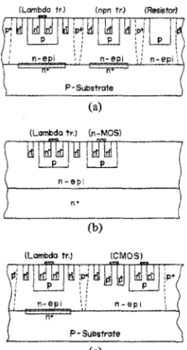
It should be noted that the starting silicon wafer should be an n/p epi-wafer for bipolar integrated-circuit fabrication with n+ buried layer and p-type diffusion isolation as shown in Fig. 5(a), where the resistor, diode, and bipolar transistor can be simultaneously fabricated. It is clearly seen that the combina- tion of the Lambda bipolar transistor with bipolar integrated circuits need only an additional noncritical mask to etch the gate oxide region of the MOSFET if low-power integrated circuits are needed. In general, this additional mask is not required, because, in the present structure, the substrate bias effect (see ( 5 ) ) is enough t o reduce the threshold voltage of the MOSFET. For the combinations of the Lambda bipolar transistor and the n-channel MOSFET integrated circuits, the p-type diffusion for isolation is not necessary, hence, five masks are necessary for AI-gate n-channel MOS integrated- circuit fabrication, as is shown in Fig. 5(b). As regard to the
simultaneous fabrication of the n-p-n Lambda bipolar tran-
sistor and CMOS integrated circuits, additional two masks are needed for the buried layer and p+ isolation, because the p channel of CMOS may interact with n+ collector diffusion of
the n-p-n Lambda bipolar transistor, as is shown in Fig. 5(c), but the additional masks are also noncritical. If the buried layer of the n-p-n Lambda bipolar transistor is not necessary
n'
(Lambda tr.1 (CMOS1
I
P-Substrate(C)
Fig. 5. (a) A structure for incorporation of an n-p-n Lambda bipolar transistor into the conventional bipolar integrated circuits. (b) A structure for incorporation of an n-p-n Lambda transistor into the conventional n-channel MOS integrated circuits. (c) A structure for incorporation of an n-p-n Lambda transistor into the conventional CMOS integrated circuits.
TABLE I
THE BASIC FABRICATION PROCEDURES OF THE DISCRETE LAMBDA BIPOLAR TRANSISTOR
Strictly clean the n-type (or n/n+) silicon wafer surface.
Thermally grow a layer of SiOl about 8000n".
Use the first mask to define the base diffusion region of n-p-n
transistor.
Boron predeposition ( 9 5 O O C j .
Boron glass removal.
Boron drive-in (12OO0Cj and the silicon oxide growth.
Use the second mask to define the emitter and the collector
windows of the n-p-n transistor, and the drain window of n-channel
MOSFET.
Phosphorous predeposition (lOOO°Cj. Phosphorous-silicate glass removal.
Phosphorous drive-in (l05O0C) and silicon oxide growth.
Use the third mask to remove the n-channel gate oxide within
the base, and clean the gate surfaoe.
Thermally grow a silicon dioxide of 1 0 0 0 ~ with dry O 2 at 95OoC.
Phosphcrous-silicate glass gettering, glass removing, and anne- al ing
.
U s e the fourth mask to d e f m e the base, the emitter, the ccl- lector ccntact windows.
A 1 metalizaticn (E-beam) .
Use the fifth mask to define the metalization pattern.
sintering and testing.
for performance requirements in MOS and CMOS integrated circuits, one mask can be saved. For discrete Lambda bipolar- transistor fabrication, the n-type wafer or n/n" epitaxial wafer can be used to fabricate a high-power Lambda bipolar tran-
418 IEEE TRANSACTIONS ON ELECTRON DEVICES, VOX,. E ? - 2 7 , NO. 2 , FEPRIJARY 1980
sistor with interdigitated structure. It is clearly seen that the Lambda bipolar transistor can be easily incorporated with the existing integrated-circuit technologies. It should also be noted that ion implantation, silicon gate, and SOS technol- ogies also may be used for high-performance applications.
IV. EXPERIMENTAL RESULTS AND THEORETICAL COMPARISONS
The typical characteristics of the common-emitter config- uration of the fabricated n-p-n Lambda bipolar transistor are shown in Fig. 6. The starting wafer is the n-type silicon sub- strate with (1 11) surface orientation and sheet resistivity of 3-5 S2 cm. For the n-channel Al-gate MOSFET, the effec- tive channel length L is about 19 pm, the channel width Z is 75 /.m, the gate oxide to, thickness is 1000
8,
the depth of the source and the drain n' diffusionW E
(equal to the depth of emitter diffusion) is about 3 pm, the base junction depth is about 6 p n , the threshold voltage without substrate bias is about 7.8 V which is roughly in agreement with the surface concentration of 4 X 10"/cm3 and surface fixed charge of 5 X 10"/cm2 for ( 1 11) silicon surface orientation. For the n-p-n bipolar transistor within the Lambda bipolar transistor, the base junction depth is about 6 pm and the emitter junction depth is 3 pm, which gives the effective basewidth of 3 pm, and the sheet resistivities of the base and the emitter are es- tablished to be 170 and 2 n/U, respectively. The common- base- output characteristic of the same device is also shown in Fig. 7.Since the substrate bias effect increases with the base current drive for high base surface concentration, the onset voltage of the negative differential resistance is much reduced as the base current drive 1; is increased, no matter how high the threshold voltage of the n-MOS at zero bias is. Although the surface concentration of the n-MOS is high, which will give lower source-drain breakdown voltage, the emitter-base voltage drop
VBE,sat of the n-p-n transistor is only 0.8 V which is just the source-drain voltage of the MOSFET, hence, the n-channel MOS will never be in breakdown for a practical base diffusion process. This is one of the merits of the Lambda bipolar tran- sistor configuration. The breakdown voltage of the Lambda
transistor is completely controlled by the following factors: n-channel MOS gate oxide dielectric field strength and oxide thickness, and the base-collector junction breakdown of the n-p-n bipolar transistor. Hence high breakdown voltage of the Lambda bipolar transistor can be easily obtained by lowering the collector doping concentration and increasing the n-MOS gate oxide thickness. In the present case, the emitter-to- collector breakdown voltage, SVcE,, is about 100 V.
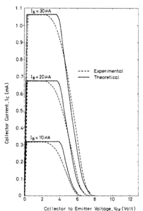
In order to check the theoretical calculations presented in Section 11, the circuit model with nonlinear
p
of 32, 34, and 37 for 1; of 10,20, and 30 pA, respectively, and the empirical parameters of K = 180 and r = - 0.48 for effective n-channel surface mobility, and the collector series resistance ofrsc
=466 S2, are used t o fit the experimental data as shown in Fig. 8.
The slight discrepancy for the characteristic of low base cur- rent drive 1; is mainly due t o the ambiguous definition of the threshold voltage and the subthreshold effect of n-channel IMOSFET. Hence, the threshold voltage V& defined by ( 5 ) is
Fig. 6 . The common emitter output characteristic of the fabricated Lambda bipolar transistor operated with the current steps driven at the base terminal B'.
Fig. 7. The common-base output characteristic of the fabricated n-p-n Lambda bipolar transistor as shown in Fig. 6 .
1 . t 1 0 0.9 O B 0.7
-
4 E-
0.6 I c ? 0.5 L 3 2 0 4s
L a8-
-
0.3 0.2 0.1 0 r- 2 4 6 8 1 0 1 2Collector to Emitter Voltage,VcE(Volt)
2 4 6 8 1 0 1 2
Collector to Emitter Voltage,VcE(Volt)
Fig. 8. Comparisons between the collector-emitter output character- istic obtained from the dc analysis (solid lines) with the experimental curves (dotted lines).
not accurate for the best fit at low base current drive, but is more accurate as the base current is high. In regard to the e m pirical relation of surface mobility, the positive coefficient of
WU AND WU: LAMBDA BIPOLAR TRANSISTOR 419
gate voltage dependence shows that electrons in the inver- sion layer of the n-channel MOS are mainly scattered by sur- face impurity below the peak mobility curve as indicated by other authors [19] , [20] for high-threshold-voltage n-channel MOSFET with substrate bias. It should be noted that the gen- eral agreement for high base current drive is good for the present theory.
V. CONCLUSION
A new integrated three-terminal voltage-controlled negative-
resistance transistor, the Lambda bipolar transistor, obtained by an integrated device consisting of a bipolar transistor
merged with a MOSFET of the same carrier type, is studied both experimentally and theoretically. It is shown that the Lambda bipolar transistor can easily be incorporated into the existing fabrication technologies of bipolar transistor inte-
grated circuits and MOS integrated circuits. It has a remark-
ably simple structure, small dimensions, and a controllable negative-resistance region. The sectional model developed is in good agreement with the experimental characteristics observed with the fabricated Lambda bipolar transistor. A wide variety
of applications [21] for the Lambda bipolar transistor, such as: oscillator, switch, amplifier, and memory function, are ex- pected. The detailed device ac performance, characterization, and system applications are still being explored and will be ad- dressed in future publications.
REFERENCES
[ l ] G. Kano and H. Iwasa, “A new A-type negative resistance device of integrated complementary JFET structure,” IEEE Trans. Electron Devices (Corresp.), vol. ED-21, pp. 448-449, July 1974. [ 2 ] G . Kano, H. Iwasa, H. Takagi, and I. Teramoto, “The Lambda
diode: A versatile negative-resistance device,” Electronics, pp. 105-109, June 26,1975.
[ 3 ] H. Takagi and G. Kano, “Complementary JFET negative-resis- tance devices,” IEEE J Solid-state Circuits, vol. SC-10, no. 6, pp. 509-515, Dec. 1975.
[4] H. Takagi and G. Kano, “Dual depletion CMOS (D2-CMOS)
static memory cell,” IEEE J. Solid-State Circuits, vol. SC-12,
no. 4, pp. 424-426, Aug. 1977.
[5] A. C. Ipri, “Lambda diode utilizing an enhancement-depletion CMOS/SOS process,” IEEE Trans. Electron Devices, vol. ED-24, pp. 751-756, June 1977.
[6] S. Koike, G. Kano, A. Kashiwakura, and I. Teramoto, “New two- terminal C-MOS memory cells,” IEEE Trans. Electron Devices, vol. ED-23, pp. 1036-1041, Sept. 1976.
[7] B. J. Baliga, D. E. Houston, and S. Krishna, “GAMBIT: Gate modulated bipolar transistor,” Solid-Stale Electron., vol. 18, [8] B. J. Baliga, “An improved GAMBIT device structure,” IEEE Trans. Electron Devices (Corresp.), vol. E:D-25, pp. 1411-1412, Dec. 1978.
[9] T. Mimura, “Voltage-controlled DNR in unijunction transistor structure,” IEEE Trans. Electron Devices (Corresp.), vol. ED-21, [ l o ] K. Lehovec and R. Zuleeg, “Negative resistance of a modified
imuLated-gate field-effect transistor,” Proc. IEEE (Lett.), vol. 62, [ l l ] R. E. Thomas, W. A. Chin, and R. F. Haythornthwaite, “A sur-
face-controlled negative impedance transistor,” in Proc. o f h t . Electron Devices Meet. (Washington, DC), paper 17.2,1973. [12] R. E. Thomas, R. F. Haythornthwaite, and W. A. Chin, “The
NEGIT: A surface-controlled negative impedance transistor,” IEEE Trans. Electron Devices, vol. ED-24,, pp. 1010-1076, 1977. [13] C. Y. Wu and K. N. Lai, “A new integrated voltage-controlled
negative resistance device-the LAMBDA MOSFET,” Solid-state Electron., vol. 22, pp. 779-781, 1979.
[ 141 -, “Integrated A-type differential negative resistance MOSFET device,” IBEE J. Solid-State Circuits, vol. SC-14, pp. 1094-1101, Dec. 1979.
[15] C. Y. Wu, K. N. Lai, and C. Y. Wu, “Generahzed theory and realization theory of voltage-controlled negative resistance MOS device (LAMBDA MOSFET),” to be published in Solid-state Electron.
[ 161 C. Y. Wu and C. Y. Wu, “A new voltage-controlled negative dif- ferential resistance device-the LAMBDA bipolar transistor,” to be published in Solid-state Electron.
[17] A. S. Grove, Physics of Semiconductor Devices. New York: Wiley, 1969, pp. 218-220.
[ 181 P. Richman, MOS Field Effect Transistoips and Integrated Circuits. New York: Wiley, 1973, p. 40.
[19] T. Sato, Y. Takeishi, and H. Hara, “Mobility anisotropy of elec- trons in inversion layers on oxidized silicon surfaces,” Phys. Rev. B , vol. 4, no. 6, pp. 1950-1960, Sept. 1971.
[20] F. F. Fang and A. B. Fowler, “Transport properties of electrons in inverted silicon surfaces,” Phys. Rev., vol. 169, no. 3, pp. 613-631, May 1968.
pp. 937-941,1975.
P P . 604-605.,,Se~t_274z_
pp. 1163-1165,A~g. 1974.