IEEE ELECTRON DEVICE LETTERS, VOL. 30, NO. 3, MARCH 2009 231
Degradation Mechanism of Poly-Si TFTs
Dynamically Operated in OFF Region
Ya-Hsiang Tai, Member, IEEE, Shih-Che Huang, and Po-Ting Chen
Abstract—This letter reports the study of the reliability
behav-ior of poly-Si thin-film transistors (TFTs) with the pulsed gate volt-age lower than the threshold voltvolt-age. First, the equivalent circuit model for poly-Si TFT is proposed. Considering the voltage drop for each element in the circuit model during the OFF-region gate dynamic stress, it is proposed that the main voltage drop occurs at the source and drain junctions, which could in turn degrade the device during stress. Based on this assumption, the gated p-i-n device fabricated on the same glass with the identical process conditions is stressed and analyzed. The similarity between the capacitance curves of the TFTs and gated p-i-n devices after stress proves that the main reason for degradation of poly-Si TFTs under gate OFF region ac stress is the large voltage drop across the source and drain junctions.
Index Terms—AC stress, dynamic stress, poly-Si thin-film
tran-sistors (TFTs), reliability.
I. INTRODUCTION
L
OW-TEMPERATURE polycrystalline silicon (LTPS) thin-film transistors (TFTs) have higher device mobility than amorphous silicon TFTs due to the improved crystallinity in the active region. This enables the possibility of forming the display backplane electronics, including the in-pixel switches and the peripheral circuits simultaneously [1]. Unlike those in the pixels, gate electrodes of TFTs in driving circuits are subjected to high-frequency voltage pulses, which may toggle in the OFF region. Therefore, the degradation behaviors for dynamic operations in the OFF region should be studied in detail. Thus far, there are few studies on the reliability of poly-Si TFTs dynamically stressed in the OFF region [2]–[4]. In this letter, the equivalent circuit model for poly-Si TFT is proposed, and the voltage drop on the elements in the circuit model during stress is discussed. Based on the model, the gated p-i-n devices are fabricated, and its behavior after stress is compared with those measured from the stressed TFTs.Manuscript received September 8, 2008. First published December 31, 2008; current version published February 25, 2009. This work was supported in part by the National Science Council, Republic of China under Contract NSC 97-2218-E-009-005 and in part by the 2007 Graduate Students Study Abroad Program, National Science Council, Taiwan, under Contract NSC-096-2917-I-009-103. The review of this letter was arranged by Editor A. Nathan.
Y.-H. Tai and P.-T. Chen are with the Department of Photonics and Display Institute, National Chiao Tung University, Hsinchu 30010, Taiwan (e-mail: [email protected]; [email protected]).
S.-C. Huang is with the Department of Photonics and Institute of Electro-Optical Engineering, National Chiao Tung University, Hsinchu 30010, Taiwan (e-mail: [email protected]).
Color versions of one or more of the figures in this letter are available online at http://ieeexplore.ieee.org.
Digital Object Identifier 10.1109/LED.2008.2010784
II. EXPERIMENTS
Top gate LTPS TFTs with width/length of 20 μm/5 μm were fabricated using low-temperature process. First, the buffer ox-ide and a-Si:H films with thickness of 50 nm were deposited on glass substrates with PECVD. The samples were then placed in the oven for dehydrogenation. The XeCl excimer laser of wavelength 308 nm and energy density of 400 mJ/cm2 was applied. The laser scanned the a-Si:H film with beam width of 4 mm and 98% overlap to recrystallize the a-Si:H film to poly-Si. After poly-Si active area definition, 50-nm SiO2 and 25-nm SiNXwere deposited with PECVD as the gate insulator. Next,
the TFT gate was formed by metal sputtering and then defined by photolithography. For n-type poly-Si TFTs, the lightly doped drain (LDD) and the n+ source/drain doping were formed by PH3 implantation with dosage 2× 10¹³ and 2× 1015 cm−2 of PH3, respectively. The LDD implantation was self-aligned, and the n+ regions were defined using a separate mask. The LDD structure was not adopted on p-type devices. The p+ source/drain doping was done by B2H6self-align implantation with a dosage of 2× 1015cm−2. Then, the interlayer of SiNX
was deposited. Subsequently, dopants were activated via rapid thermal annealing while the poly-Si film was hydrogenated simultaneously. Finally, the contact hole formation and metal-lization were performed to complete the fabrication work. The slight difference between the gated p-i-n device process and the n-type TFT process is that one side of the source/drain doping was changed to p+. The gated p-i-n devices are fabricated in parallel with the TFTs on the same glass substrate to ensure identical process conditions. The typical values of the threshold voltage for the n-type and p-type fresh devices are 1.63 and
−1.88 V, respectively.
Rectangular pulses applied to the TFTs are generated with an Agilent 41501B pulse generator, and the dc stress ap-plied to the gated p-i-n device is performed by using an Agilent 4156A precision semiconductor parameter analyzer. The capacitance–voltage (C–V ) curves were measured with an Agilent E4980A precision LCR Meter.
III. RESULT ANDDISCUSSION
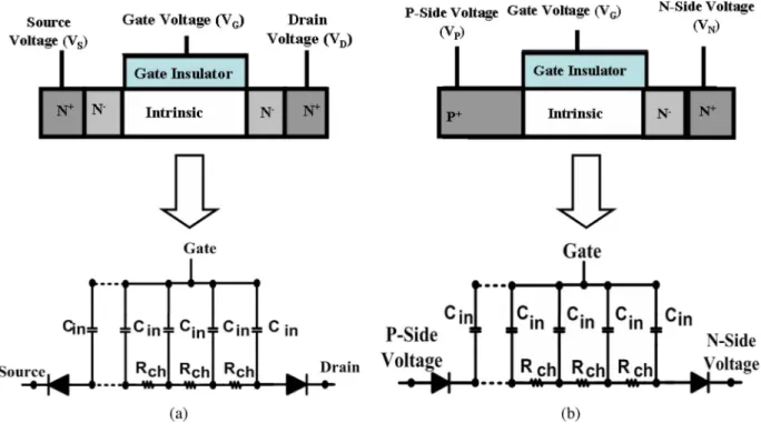
Fig. 1(a) shows the cross-sectional view and an equivalent circuit model for n-type poly-Si TFTs. Cin, Rch, and the diodes represent the gate insulator capacitance per partition, the channel resistance per partition, and the source/drain junctions, respectively. For the p-type poly-Si TFTs, the diode terminals representing the junctions are reversed. The impedance be-tween gate and source/drain can be expressed by Z = Rch + 1/j2πf Cin, where f represents the operation frequency [5].
232 IEEE ELECTRON DEVICE LETTERS, VOL. 30, NO. 3, MARCH 2009
Fig. 1. Cross-sectional view and proposed circuit model for (a) TFT and (b) gated p-i-n device.
Under dc and low-frequency operations, the impedance is dom-inated by the capacitance term, and the applied gate voltage drops across the gate insulator. Under high-frequency ac op-erations, the resistance term may not be neglected, and both the capacitance and resistance terms need to be considered. Furthermore, in the OFF region, gate voltage is below the threshold voltage, and no induced layer is formed, making Rch large and may dominate even at low frequency. Referring to Fig. 1(a), if the source and drain electrodes are grounded and the gate pulse toggles in the OFF region, the voltage drop would mainly occur across Rch and the diodes, and therefore, large voltage drop on the diodes in reverse-bias could lead to the degradation.
However, this assumption is difficult to verify because the voltage drop in the channel can hardly be probed for the TFTs in OFF region. Therefore, in this letter, the gated p-i-n device is adopted, where one side of the source/drain doping in fabricating n-type TFT is changed from N+and N− to P+. The cross-sectional view and an equivalent circuit model of the gated p-i-n device are shown in Fig. 1(b). The reason for adopting such gated p-i-n device is that this device has the similar structure to the TFTs while the channel voltage can be set from one of the electrodes with forward-biased junction. Thus, this enables us the application of reverse bias at one junction to simulate the condition of gate ac OFF region stress for poly-Si TFTs. Then, by examining the capacitance curves of the TFTs and gated p-i-n devices after stress, the afore-mentioned mechanism can be verified.
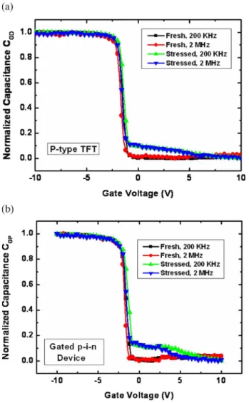
Fig. 2(a) shows the normalized gate-to-drain capacitance
CGDcurves for TFT before and after gate ac stress in the OFF region for 200 s. The stress condition is that the rectangular signal that toggles between 0 and−25 V at 500 kHz and duty cycle of 50% is applied to the gate electrode and both the source and drain electrodes are grounded. As shown in Fig. 2(a), the
Fig. 2. (a) Normalized capacitance CGDfor the n-type TFT before and after
gate ac stress in the OFF region. (b) Normalized capacitance CGNfor the gated
TAI et al.: DEGRADATION MECHANISM OF POLY-Si TFTs DYNAMICALLY OPERATED IN OFF REGION 233
Fig. 3. (a) Normalized capacitance CGDfor the p-type TFT before and after
gate ac stress in the OFF region. (b) Normalized capacitance CGPfor the gated
p-i-n device before and after stress.
frequency-dependent degradation for the capacitance behavior indicates that the main effect for the stress is bias induced state creation [6]. To verify the mechanism previously mentioned, the gated p-i-n device is dc stressed for 200 s with voltage of the gate electrode, the p-side electrode, and the n-side electrode set to−20, −5, and 20 V, respectively. The biases are chosen such that the gate voltage induces holes in the intrinsic channel and the main voltage drop occurs on the junction near the n-side electrode. Fig. 2(b) shows the normalized gate-to-n-side capacitance CGN curve for the gated p-i-n device before and after stress. For the CGNcurves before and after stress, it can be observed that after stress the CGNcurve shows similar behavior as the n-type TFT after gate ac stress. The similarity of the capacitance curves between the stressed TFT and gated p-i-n device reveals the verification of the proposed mechanism.
Fig. 3(a) shows the CGD curves for the p-type TFT before and after gate ac stress. The stress condition is that the ac gate
pulse toggles between 0 and 20 V with 50% duty cycle at 500 kHz. Source and drain electrodes are grounded, and the stress duration is 200 s. For the stressed device, the CGD curves show apparent increase for the gate voltage lower than the flatband voltage, which indicates the channel shortening effect [7]. The gated p-i-n device is also stressed in order to verify this phenomenon. The dc stress condition is that the gate voltage is 15 V, the n-side voltage is 20 V, and p-side is
−5 V with duration of 200 s. The gate-to-p-side capacitance CGP curves before and after stress are shown in Fig. 3(b). The similarity between the CGD and CGP curves for the TFT and gated p-i-n device indicates the validation of the proposed mechanism. This finding may provide important insight for the further understanding and modeling of poly-Si TFTs in dynamical operations.
IV. CONCLUSION
A circuit model for poly-Si TFT is proposed and based on the model the device degradation for the gate ac stress in the OFF region is studied. It is inferred that the voltage drop could mainly occur on the junction during stress, and the gated p-i-n device is further adopted to verify the assumption. The simi-larity between the capacitance curves for the ac-stressed TFT and dc-stressed gated p-i-n device proves the aforementioned inference. This finding would be beneficial for the further modeling and reliability designing of the poly-Si TFTs in the advanced circuitry.
ACKNOWLEDGMENT
The authors would like to thank Dr. Y. Kuo in Texas A&M University for valuable discussion.
REFERENCES
[1] Y.-H. Tai, C. C. Pai, B. T. Chen, and H. C. Cheng, “A source-follower type analog buffer using poly-Si TFTs with large design windows,” IEEE
Electron Device Lett., vol. 26, no. 11, pp. 811–813, Nov. 2005.
[2] Y. Uraoka, T. Hatayama, T. Fuyuki, T. Kawamura, and Y. Tsuchihashi, “Re-liability of low temperature poly-silicon TFTs under inverter operation,”
IEEE Trans. Electron Devices, vol. 48, no. 10, pp. 2370–2374, Oct. 2001.
[3] Y. Uraoka, T. Hatayama, T. Fuyuki, T. Kawamura, and Y. Tsuchihashi, “Reliability of high-frequency operation of low-temperature polysilicon thin film transistors under dynamic stress,” Jpn. J. Appl. Phys., vol. 39, no. 12A, pt. 2, pp. L1209–L1212, Dec. 2000.
[4] Y.-H. Tai, S.-C. Huang, and C.-K. Chen, “Analysis of poly-Si TFT degrada-tion under gate pulse stress using the slicing model,” IEEE Electron Device
Lett., vol. 27, no. 12, pp. 981–983, Dec. 2006.
[5] C. Alexander and M. Sadiku, Fundamentals of Electric Circuits. New York: McGraw-Hill, 2004, pp. 383–388.
[6] Y.-H. Tai, S.-C. Huang, C. W. Lin, and H. L. Chiu, “Degradation of the capacitance–voltage behaviors of the low-temperature polysilicon TFTs under DC stress,” J. Electrochem. Soc., vol. 154, no. 7, pp. 611–618, 2007.
[7] S.-C. Huang, H.-C. Tsao, and Y.-H. Tai, “Estimation of the effect of channel shortening for P-type poly-Si TFTs under AC stress,” in Proc. IDMC, 2007, pp. 134–137.