Ultra Low-Capacitance Bond Pad for RF Applications
in CMOS Technology
Yuan-Wen Hsiao and Ming-Dou Ker
Nanoelectronics and Gigascale Systems Laboratory
Institute of Electronics, National Chiao-Tung University, Hsinchu, Taiwan
Abstract — A low-capacitance bond pad for gigahertz RFapplications is proposed. Three kinds of on-chip inductors embedded under the traditional bond pad are used to compensate bond-pad capacitance. Experimental results have verified that bond-pad capacitance can be significantly reduced in a specific frequency band due to the cancellation effect provided by the embedded inductor in the proposed bond pad. The proposed bond pad is fully compatible to general CMOS processes without any process modification.
Index Terms — Bond pad, capacitance, signal loss, radio-frequency integrated circuit (RF IC).
I. INTRODUCTION
With the advantages of high integration capability and low cost for mass production, radio-frequency integrated circuits (RF ICs) operating in gigahertz frequency bands have been implemented in CMOS technology. However, the undesired parasitic capacitances at the input/output (I/O) pads of silicon chips often limit the high-frequency performance of RF ICs. The bond-pad capacitance should be minimized to mitigate the RF performance degradation. Moreover, on-chip electrostatic discharge (ESD) protection devices are also placed around the I/O pad, which further decrease the design budget because of the extra parasitic capacitance from the ESD protection devices [1]-[2]. Although the progress of CMOS technology enables device dimensions to shrink substantially, the bond pad size is still kept at a large enough size to ensure the bonding reliability. Therefore, the parasitic capacitance resulted from the bond pad metal and the overlapped substrate can not be reduced with the progress of CMOS technology. In some CMOS integrated RF front-ends, the bond-pad capacitance can be incorporated as a part of the matching network. Recently, several techniques were reported to reduce the bond-pad capacitance [3]-[5]. A bond pad structure realized with special layout patterns, which have smaller metal area and additional diffusion layers, had been demonstrated to have smaller bond-pad capacitance [3]. Another bond pad using the depletion-insulation structure to improve cross-talk isolation and quality factor had been presented [4].
Besides, a bond pad structure realized with semi-insulating porous silicon had also been reported to reduce the bond-pad capacitance [5].
In this paper, a new bond pad structure with embedded inductor is proposed to reduce the bond-pad capacitance. The proposed bond pad structure possesses several features. First, it is fully compatible to standard CMOS processes without any extra process modification. Second, the proposed bond pad has the same dimensions as that of the traditional bond pad without any extra area consumption. Third, the proposed bond pad has lower parasitic capacitance than that of the traditional bond pad, which is suitable for gigahertz RF applications. The proposed low-capacitance bond pad and its equivalent circuit model are presented in Sections II and III, respectively. The experimental results and discussion are presented in Section IV. Finally, conclusion is provided in Section V.
II. PROPOSED LOW-CAPACITANCE BOND PAD
In this work, a 0.13-μm 1P8M CMOS process is used. The typical bond pad provided by the foundry is implemented with eight metal layers (from metal 1 to metal 8). Since the parasitic capacitance of the bottom metal layer (metal 1) and the overlapped substrate is too large for gigahertz RF applications, the lower metal layers were often removed from the bond pad in order to reduce the bond-pad capacitance. However, using only the top metal layer (metal 8) to implement bond pads causes some concerns on bonding reliability. To compromise the dilemma between bond-pad capacitance and bonding reliability, the reference bond pad used in this work is realized with only top three metal layers, which are metals 8, 7, and 6 in the 0.13-μm CMOS process.
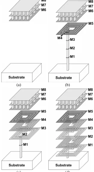
The reference bond pad, the proposed bond pad with one-layer inductor (implemented with metal 5), three-layer stacked inductor (implemented with metals 5, 4, and 3), and five-layer stacked inductor (implemented with metals 5, 4, 3, 2, and 1) are illustrated in Figs. 1(a) –1(d), respectively. In the proposed bond pad structure, the
chip stacked inductor [6] is embedded under the metal plate of the reference bond pad. Since the on-chip stacked inductor is implemented within the region of the metal plate of the reference bond pad, the proposed bond pad occupies the same chip area as the reference one, which is 70 μm × 57 μm in this work. The bond pads with three kinds of inductors, which are one-layer inductor, three-layer stacked inductor, and five-three-layer stacked inductor, have been designed in the experimental test chip to investigate capacitance reduction. The inductors are realized with the metal-track width of 4 μm, metal-track spacing of 1 μm, and 5 turns. The inductor designed in such architecture is used to increase the inductance under the pre-specified region (the region of the reference bond pad) to cancel the bond-pad capacitance resulted from the metal plate and the overlapped substrate.
(a) (b)
(c) (d)
Fig. 1. (a) Reference bond pad. (b) Proposed bond pad with 1-layer inductor. (c) Proposed bond pad with 3-1-layer stacked inductor. (d) Proposed bond pad with 5-layer stacked inductor.
Fig. 2 shows the layout top view of the test pattern used to extract the bond-pad capacitance. The layout pattern of Ground-signal-ground (G-S-G) pads with 150-μm pitch was adopted to facilitate on-wafer measurement. The guard ring is implemented to encircle the proposed bond pad and connected to a signal pad for measurement. With the guard ring connected to the substrate, the bond-pad capacitance between the top metal plate and substrate can be characterized by the two-port S-parameter measurement.
Fig. 2. Layout top view of the test pattern to extract the bond-pad capacitance.
III. CIRCUIT MODEL OF PROPOSED BOND PAD
In order to acquire the characteristics of the proposed bond pad during circuit design, the equivalent circuit model of the proposed bond pad has been developed, as shown in Fig. 3. The equivalent circuit model of the proposed bond pad consists of three parts, which are the parasitic capacitance between the metal plates of the bond pad and substrate, coupling effect between the metal plate and stacked inductor, and the stacked inductor model. In the first part, CP represents the parasitic capacitance
between the metal plates of the bond pad and the substrate. In the second part, CC1, CC2, R1, and R2 denote the
coupling effect between the metal plates of the bond pad and the stacked inductor. The third part is the stacked inductor model, which is provided by the foundry. CF
denotes the parasitic capacitance between the metal layers in the stacked inductor. LS and RS are the inductance and
series resistance of the stacked inductor, respectively. Cox1
and Cox2 represent the capacitance between the stacked
inductor and the substrate. CSUB and RSUB represent the
parasitic capacitance and parasitic resistance of the substrate, respectively. The simulated bond-pad capacitance in the proposed model will be compared with the measured bond-pad capacitance in Section IV.
Fig. 3. Equivalent circuit model of the proposed bond pad. IV.EXPERIMENTAL RESULTS AND DISCUSSION
The proposed bond pads with one-, three-, and five-layer stacked inductors, as well as the reference bond pad, were fabricated in the same silicon chip in a 0.13-μm 1P8M CMOS process. The two-port S-parameters of the fabricated bond pads were characterized by on-wafer measurement with the Cascade Air Coplanar G-S-G microwave probes and the Agilent 8510C network analyzer.
A. Measured Bond-Pad Capacitance
In the bond-pad capacitance measurement, port 1 and port 2 of the network analyzer were connected to the proposed bond pad and the signal pad shown in Fig. 2, respectively. With the conversions between two-port S-parameters and Z-S-parameters, the bond-pad capacitance (Cpad) was extracted as Cpad = –1 / [ω Im(Z11)], where Z11
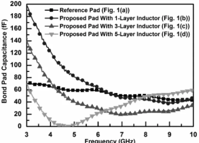
parameter is the impedance seen from port 1 with port 2 open. Fig. 4 shows the extracted bond-pad capacitances among the fabricated bond pads under different frequencies. As shown in Fig. 4, the reduction on the bond-pad capacitance is more significant when the embedded stacked inductor is realized with more metal layers. With a five-layer stacked inductor in the proposed bond pad, the bond-pad capacitance can be even reduced to almost 0 fF at a specific frequency band (4.3 ~ 4.8 GHz). The bond-pad capacitance is reduced due to the positive reactance contributed from the embedded inductor. For example, the bond-pad capacitance of the proposed structure with one-, three-, and five-layer stacked inductors can be reduced 2.9%, 58.9%, and 49.3% from the original value (the reference pad) at 6.5 GHz, respectively. The frequency band in which the bond-pad capacitance is reduced can be adjusted or extended by designing the embedded inductor.
B. Measured Signal Loss of the Proposed Bond Pad The measured signal losses among the fabricated bond pads are shown in Fig. 5. In the signal loss measurement,
port 1 and port 2 of the network analyzer were both connected to the top metal plate of the bond pad. The signal loss was obtained from the measured S21 parameter
with the relation of Loss (dB) = – [S21 (dB)]. Since the
impedance of the five-layer stacked inductor is higher than those of the one- and three-layer stacked inductors, the proposed bond pad with the five-layer stacked inductor has the least loss, while the proposed bond pad with the one-layer inductor has the most loss among the three kinds of proposed bond pads. From 3 to 10 GHz, the proposed bond pad with the five-layer stacked inductor has a loss less than 0.65 dB. Because the inductor was connected to substrate in the proposed bond pad structure, the proposed bond pad has more loss than that of the reference bond pad. However, since all I/O pads need to be accompanied with ESD protection circuits, the loss of the proposed bond pad will not be the critical part at the input or output nodes because of the larger signal loss caused by the on-chip ESD protection devices.
Fig. 4. Extracted bond-pad capacitances among the fabricated bond pads under different frequencies.
Fig. 5. Measured signal losses among the fabricated bond pads under different frequencies.
C. Comparison Between Simulated and Measured Results To verify the equivalent circuit model of the proposed bond pad shown in Fig. 3, the simulated bond-pad capacitance in the proposed equivalent circuit model was compared to the measured bond-pad capacitance. The dimensions of the passive components used in the circuit model of the proposed bond pad with 5-layer inductor except the stacked inductor are listed in Table I. The simulated and measured bond-pad capacitances of the proposed bond pad with the 5-layer stacked inductor are compared in Fig. 6. The simulation tool used to simulate the bond-pad capacitance was Ansoft Designer/Nexxim. As shown in Fig. 6, the measured bond-pad capacitance agrees well with the simulated bond-pad capacitance from 3 GHz to 10 GHz. Thus, the circuit model of the proposed bond pad is appropriate to model the bond-pad capacitance. To refine the circuit model for the proposed bond pad comprehensively, more test devices will be needed to enhance the accuracy of this circuit model for different frequency bands.
TABLE I
DIMENSIONS OF PASSIVE COMPONENTS USED IN THE
BOND-PAD MODEL WITH 5-LAYER STACKED INDUCTOR
Fig. 6. Comparison of bond-pad capacitance among the simulated result and measured result.
At 5 GHz, the capacitance of the proposed bond pad with the five-layer stacked inductor is only 3.15 fF, which is quite small. Therefore, the proposed bond pad is suitable for gigahertz RF applications. Moreover, the frequency at which the capacitance of the proposed bond pad is minimum can be adjusted by changing the dimensions of the stacked inductor and the metal plates of
the bond pad. To mitigate the impact of the bond-pad loss, the proposed bond pad can be co-designed with on-chip ESD protection devices. For example, the impedance isolation technique can be used to optimize the RF characteristics at the input and output nodes, which have the bond pad and the on-chip ESD protection devices [7].
IV.CONCLUSION
By inserting a stacked inductor under a conventional bond pad, the proposed bond pad performs low parasitic capacitance. The experimental results have proven that the embedded inductor can be used to reduce the bond-pad capacitance. With the bond-pad model developed in this work, the capacitance of the proposed bond pad can be taken into consideration during the design phase of the RF ICs. The proposed low-capacitance bond pad structure, achieved by layout modification, is fully compatible to general CMOS processes for RF applications.
ACKNOWLEDGEMENT
The authors would like to thank Ansoft Corporation for the support of simulation tool.
REFERENCES
[1] M.-D. Ker, Y.-W. Hsiao, and B.-J. Kuo, “ESD protection design for 1-to-10 GHz distributed amplifier in CMOS technology,” IEEE Trans. Microw. Theory Tech., vol. 53, no. 9, pp. 2672–2681, Sep. 2005.
[2] M.-D. Ker, W.-Y. Lo, C.-M. Lee, C.-P. Chen, and H.-S. Kao, “ESD protection design for 900-MHz RF receiver with 8-kV HBM ESD robustness,” in IEEE Radio Frequency Integrated Circuits Symp. Dig., 2002, pp. 427– 430.
[3] M.-D. Ker, H.-C. Jiang, and C.-Y. Chang, “Design on the low-capacitance bond pad for high-frequency I/O circuits in CMOS technology,” IEEE Trans. Electron Devices, vol. 48, no. 12, pp. 2953–2956, Dec. 2001.
[4] S. Lam, W. H. Ki, and M. Chan, “High-isolation bonding pad with depletion-insulation structure for RF/microwave integrated circuits on bulk silicon CMOS,” IEEE MTT-S Int. Microw. Symp. Dig., 2002, pp. 677–680.
[5] K. Chong and Y.-H. Xie, “Low capacitance and high isolation bond pad for high-frequency RFICs,” IEEE Electron Device Lett., vol. 26, no. 10, pp. 746–748, Oct. 2005.
[6] A. Zolfaghari, A. Chan, and B. Razavi, “Stacked inductors and transformers in CMOS technology,” IEEE J. Solid-State Circuits, vol. 36, no. 4, pp. 620–628, Apr. 2001. [7] M.-D. Ker, C.-I. Chou, and C.-M. Lee, “A novel LC-tank
ESD protection design for giga-Hz RF circuits,” in IEEE Radio Frequency Integrated Circuits Symp. Dig., 2003, pp. 115–118.