Study of a common deep level in GaN
Tzu-Chi Wen*a, Shih-Chang Leea, Wei•-I Leea, Jen-Da Guob, Ming-Shiann Fengc
aDepament of Electrophysics and Microelectronics and Information Systems Research Center, National
Chiao Tung University, HsinChu, Taiwan.
bNtil Nano Device Laboratory, National Chiao Tung University, HsinChu, Taiwan.
CJtitt of Materials Science and Engineering, National Chiao Tung University, HsinChu, Taiwan.
ABSTRACT
A deep level with the activation energy around O.45—O.6eV has persistently appeared in GaN samples grown by hydride vapor-phase epitaxy, organometallic vapor-phase epitaxy and molecular beam epitaxy. However, the origin of this deep level still remains unclear. In this study, we investigated this deep level trap E2 of GaN films by using deep level transient spectroscopy. The GaN films were grown by a conventional low pressure organometallic vapor-phase epitaxy technique with different V/Ill ratios. Frequency-dependent capacitance measurement was performed to determine the mostproper frequency for capacitance measurements Capacitance-voltage measurements were then applied to obtain the canier concentrations. The carrier concentration became higher as the flow rate of NH3 got lower. The deep level E2 is found in GaN samplesgrown with higher V/Ill ratios. The trap concentration of level E2 increased with increasing NH3 flow rate. Compared with the theoretical prediction ofthe nitrogen antisite level in GaN, the level E2 was believed to be related to nitrogen antisites. Keyword GaN, deep level, organometallic vapor-phase epitaxy, V/Ill ratios, frequency capacitance, antisite defect, DLTS
INTROI)UCTION
Group 111-V mtrides have wide bandgaps varied from 1.9eV, of InN, to 6.3eV, of A1N, and been promising materials for blue and ultraviolet optoelectronic devices1, high temperature, and high power transisors23, and solar-blind ultraviolet detectors.4
However, the progress of GaN technology has often been limited by material quality, such as high defect densities.
Therefore, it is important to investigate the deep level traps in GaN. Deep-level transient spectroscopy (DLTS) and transient capacitance methods have been used to characterize the deep level traps in GaN grown by hydride vapor-phase epitaxy (HyPE), organometallic vapor-phase epitaxy (OMVPE) and molecular beam epitaxy (MBE). Several deep level centers in n-GaN with activation energies ranging from 0.14-1 .63eV have been reported5". Among them, a deep level with the activation energy around O.45-O.598eV has been observed in samples grown by different techniques5'6'7'9"°. The origin of this deep level still remains unclear. In the present study, we characterized deep level traps of two sets of GaN filmsby using deep-level transient spectroscopy (DLTS) and transient capacitance method.
EXPERIMENT
Two sets of n-type GaN film were discussed in this study. The set I, fabricated by AXTRON planetaryreactor, contained about 4 im thick Si-doped GaN layer (labeled Ri). The set II were prepared by a conventional lowpressure OMVPE, and the thickness ofundoped GaN film was about 2gm. The detail growth procedure had been described elsewhere.'2 The Set II, in brief, was grown by a conventonal low pressure OMVPE reactor with trimethylgallium (TMG)as the column III precursor, and NH3 as the column V precursor, respectively. A thin (500A) GaN buffer layer was deposited on c-plane sapphire substrate at 525 usingTMG and NH3, and GaN film was then grown at 1050 . TheGaN films, set II, was grown with
different V/Ill ratios.
The flow rate of NH3 were 2500 sccm 2000 sccm 1500 sccm,
labeledPt/Au and Au were used as Schottky contact metal on set I and set II, respectively. Aluminum was deposited a large area on the front surface as an ohmic contact. The current-voltage characteristic of Schottky diode at room temperature was well behaved. To determinate the most proper frequency of capacitance-voltage (C-V) and transient capacitance measurements, conventional capacitance-frequency (C-F) measurement were employed. Capacitance-voltage (C-V) measurements, to obtain the carrier concentration, were taken at different temperature to identify whether the carrier concentration was changing with temperature. A DLTS spectrometer by SULA Technology and a liquid-nitrogen cryostat operated in the temperature range between 90 and 530Kwas used DLTS measurements. For the DLTS measurement, a 100 ms wide pulse at O.3V was applied
to fill the electron traps in GaN. A reverse bias of—3V was applied to remove electrons from the deep level in the depletion region, and the capacitance transient was detected by a 1MHz capacitance meter. The transient capacitance was measured by using a HP4 1 94 impedance analyzer. The most proper measurement frequency used to do the transient capacitance
measurements were indicated form C-F measurement.
RESULTS AND DISCUSSION
The response of parallel capacitance (Cr) to the frequency of GaN2500, at different temperature, is demonstrated in Fig.1 .A Schottky diode can be simulated by a simple series RC alternating circuit. The charging and discharging of trap in low frequency can follow the input signal, while at higher frequency series resistance would affect on the result of capacitance. The abrupt increasing of capacitance at lower frequency, as shown from frequency-capacitance measurement, indicated that there are deep level traps in GaN films. According to Fig. 1 the range that the parallel capacitance do not vary with modulation frequency is around 1 0—.1 O4Hz.
The most proper capacitance-voltage measurement frequency of
GaN2000 GaN 1500 are 5KHz 1OK}Iz as suggested by C-F measurement. Figure 2 shows the carrier concentration of set II varies with measuring temperature. As the flow rate of NH3 getting lower, the free carrier concentration became higher as indicated in Fig. 2. The large background carrier concentration is usually regarded to be caused by the large amount of nitrogen vacancy'3. The carrier concentration of Ri is 1.184x 10¹⁷ (cnf3) from the similar measurement.
Fig. 2 Carner concentration of set II varied with measurement temperature. Lower the NH3 flow rate higher carrier concentration as indicated in Fig. 2. The large background carrier concentration is usually regard to cause by the big amount of nitrogen vacancy.
415K 84K 1 .80e-9 1 .60e-9 1.40e-9 1.20e-9 1 .OOe-9 8.OOe-1C
0
6.OOe-1C 4.OOe-1C 2.OOe-1C 0.0c Frequency (1/sec)Fig. 1 The response of parallel capacitance to frequency of GaN2500 at different temperature. The abrupt increasing of C, at lower
frequency was caused by deep level traps in GaN films, and the proper measurement frequency of GaN2500 was around 1 0-..i O4Hz.
3e+17
3e+17
le+2 le+3 le+4 le+5 le+6 le+7
E
0
2e+170
2e+17 00
0
le+17 CD0
5e+16 0 GaN2500 GaN2000 GaN1 500 0 100 200 300 400 Temperature (K) 500The results ofDLTS spectra ofRi are presented in Fig.3 with the emission rate window which were set as 23.26 s' and 46.52 s_i. Two distinct levels, labeled E2 and E4, were clearly observed on RI . Theactivation energy, \E, and the electron capture cross section, o of each deep level traps were extracted from Arrenius plots of 1og(Dt) versus 1 000/T, where r is the capacitance transient time constant deduced from the windows setting of the DLTS system and T is the corresponding temperature. A slop of linear least square fit to each set of data obtains the activation energy of each deep level. The characteristics of level E2 and E4 are listed in Table 1. Arrhenius plots reveal that level E2 was closed to the level with activation energy of 0.49eV found by Götz et al.5, 0.58eV report by Hacke et al.6, 0.49eV reported by Lee et al.7, 0.598eV reported by Haase et al.9, and 0.578eV reported by Wang et al.t0 Similarly, level E4 was closed to 1.10eV reported by Chen et al.8, and the 0.961eV reported by Wang et al.'°
CD -4 0) C,) (J)
-J
0
Temperature (K)Fig. 3 DLTS spectrum measured on the sample Ri with emission rate windows of 23.26' and 46.52.1.
Table I. Characteristic of deep-level E2 and E4 measured by DLTS in the GaN sample Set I (Ri)
Sample (
SetI,R1
Trap)
(E2) Nd (crn3)i.i84xiOi7
N (cm3)
NE2=4.258x10'6
AE (eV)0.556
(cm2)
1.244x10¹⁸ (E4) NE3 =6.011x10'
1.0183.310x10
To measure the transient capacitance, the reverse bias voltage of -2V was first employed to remove electrons from
deep level traps in the depletion region. The capacitance was decreased immediately as the schottky diode was
reverse biased, then the capacitance was increased exponentially to a constant value. To extract the time constants
.t for a given temperature the least square fit of an exponential function was employed.8 Sample GaN1500 reveals
only two levels, labeled as E3 and E5 Three majority traps, labeled as E2, E3 and E5, are observed in GaN2000.
2 0 -2 -6 -8 -10 -12 E4 E2 rate window:23.26 s1 rate window:46.52s1 0 100 200 300 400 500 600
for E2
in
sample GaN2000 is 0.554eV and 5.905
x1016cm2 which correspond to the defect level E2 found in Set Ias illustrate in Arrhenius plots. The activation energy and capture cross-section for E3 of sample GaN2000 is
0.649eV and 7.169x1020cm2. It close corresponded to 0.665eV reported by Hacke et al.6, 0.6eV measurement by
Chen et al.8, 0.670eV found by Haase et al.9, 0.657eV found by Wang et
and 0.62eV reported by Fang et
11
• The
activation energy AE and capture cross-section
for E5 in sample GaN1500 is 1 .342eV and 1 759x 10'3cm2. Level E5 is similarly to the 1.44eV reported by Lee et al.7 and 1.27eV reported by Chen et al.8 The
concentration of deep level traps, n, are obtains from the capacitance transient height, assuming uniform trap
distribution. The traps concentration of set II is demonstrated in Table 2.
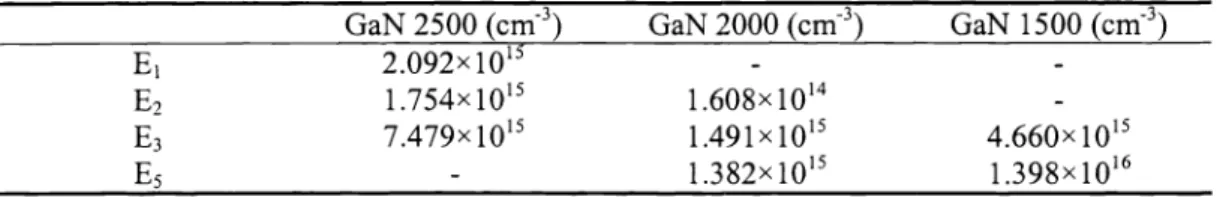
Table 2. The trap concentration of set II
GaN 2500 (cm3)
GaN 2000 (cm3)
GaN 1500 (cm3)
E1
2.092x10'
E2 1.754x10¹⁵
1.6O8x1O'
-E3
7.479x1O'
1.491x1O'
4.66Ox10'
E5
-
1.382x10'
1.398x10¹⁶The fact that level E2 appears in both samples grown by different MOCVD reactors, and different growth techniques, i.e. MOCVD, HVPE, and MBE, indicates that level E2 is originated either from a native defect or a common impurity during the growth of GaN film. The trap concentration of level E2 increases as raising the NH3 flow rate. This increment implies that level E2 is associated with either the increasing of nitrogen atoms or decreasing the gallium atoms. If level E2 is associated with Ga vacancy, then the trap concentration of E2 should be increased as the carrier concentration is decreased. It is contradictory with the results of C-V measurement. Dow and Jenkins14 calculated the deep level trap associated with Ga vacancy was acceptor like. However, the activation energy of E2 is closed to conduction band, and it is donor like. The deep
level traps for nitrogen substitution on Ga site below the conduction band 0.54eV, as indicated by Dow and Jenkins'4, was close corresponding to the activation energy of E2. In addition, Haase et al.9 demonstrated that deep level E2 could be generated by nitrogen implantation and subsequently removed by thermal annealing. Therefor, level E2 is interpreted as a result of the N-antisite defect.
The defect level E5, which also found in samples grown by different techniques, indicated it might due to a native defect or a common impurity within the grown process. The broad photoluminescense emission band near 560nm15 and broad cathodluminescence band near 520nm'6 is thought as a result of oxygen in GaN. Chen et al.8 have suggest that level E4 may be due to the oxygen impurities substitution on Ga site. The theoretical calculation the deep level of oxygen on Ga sites is 1 .27eV, while it closed to the activation energy ofE5. Thus level E5 is believed to be related oxygen impurities on Ga site.
CONCLUSION
In summary, two different sets of GaN films, grown by different organometallic vapor phase epitaxy (OMVPE), are investigated in this study. DLTS and transient capacitance are utilized to characterize the deep center in GaN layer. Two distinct levels with activation energy E2=0.556eV and E4=1.Ol8eV are clearly observed on sample Set I. Four majority-carried traps were found in sample set II, as mention above. Trap E2 is believed to relate with nitrogen antisite defect, since the trap concentration increases as NH3 flow rate increases.
ACKNOWLEDGMENTS
The authors would like to thank Dr. J.K. Ho at Industrial Technology Research Institute for crystal growth. This work was supported in part by the National Science Council ofthe R.O.C under Grant No. NSC89-2112-ll-009-Oll
(686t)
Lt
£:
6
HAJ
S/qd 'MOGG
I
SUDIUOfJ
t'T (z66T) LEZI 01 H •jOUOL'
•PS°A
•f '3o)II0JA[II
PU
!'S
S
•:i
'89cL
(966t)•WJ
Si4qjddy
'uoH
JT •fPU
'UsJ
•S •f 'Oflo •U •f'&Id
SN
'RID3
•D 'UT'-J •d3
'UIJ
3Q
'3jOO'J M ''-'!)I7
'UEJV
AJ)JT3OHP
H 'oopoj,4jdd
SAq
-T'1'U
LLZZ (g661)Oz
•t
I (8661) IRI
'U
•UO1Siq
idd
',opo
•H AO1)jZXO lçT 'UIT){4\
'A
1.I
'1I
S S'A
S '1'8EU
Q3
01 (9661)czc
'691
SAqjdd
'ioziq
H
pu
•JAI ZOIjOI
'IH
'A 'UUJQQ 'V 'JTui){'j
'pI,uqDS'F
'SH
.0
'6 '(9661)018'l
'jddy
"Si'q
-'d
'
'cE'j
'udç'8uoj
uuqs-u
pu
oo'j-i
'8unH
uA-uM
'ujj
unqj-i
'UTQ8Ud-UUf
'8 '(c661) JUT 'L9'WI
'SAIJd'jdd
'8UJ
'S'J\
pu
OnD'
'
'UflH
'D '1.'i
i
'jddy
'S/4d
'9Lt'0
'(t'661) 'ç ')1c!J,\1{
U1
OWOEp1 ')J'PI'S
'N'flSWRH
'uiqoidq
'1
')fD}
'd 9 '(t'661)£9i
'9
'WI
'SJd
'jdcty'D[sy
'j
pu
ouUIy'H
'uos4of
'N'zoo
'M'c
'(66T)
LI6Z '09 'SAqd'jddy
'ZJJO)J'
'
UE'UI8rnSEJ[
]A
'AOHUA
'JA['f
'UOSJo'1
J
'1!UZfl{ 'N'
'uq)Jjisy
'j,
j
E)
'UOtj) 'JA'y
'UEtJ)J'f
'
'8UEM')
'f
'm'S
'TAT 'S 'JiltiS 'H'T'd
jddy
'SAq4J
'69
176L '(9661)'(9661) 6ZZT '69