Spatially and temporally resolving the degradation of n-channel poly-Si thin-film
transistors under hot-carrier stressing
Ming-Hsien Lee, Kai-Hsiang Chang, and Horng-Chih Lin
Citation: Journal of Applied Physics 101, 054518 (2007); doi: 10.1063/1.2710302
View online: http://dx.doi.org/10.1063/1.2710302
View Table of Contents: http://scitation.aip.org/content/aip/journal/jap/101/5?ver=pdfcov Published by the AIP Publishing
Articles you may be interested in
Stability of n -channel a Si : H nc Si : H bilayer thin-film transistors under dynamic stress J. Appl. Phys. 103, 084514 (2008); 10.1063/1.2903445
Effective density-of-states distribution of polycrystalline silicon thin-film transistors under hot-carrier degradation J. Appl. Phys. 102, 054508 (2007); 10.1063/1.2777804
Effects of grain boundaries on performance and hot-carrier reliability of excimer-laser annealed polycrystalline silicon thin film transistors
J. Appl. Phys. 95, 5788 (2004); 10.1063/1.1699504
Photon emission and related hot-carrier effects in polycrystalline silicon thin-film transistors J. Appl. Phys. 85, 6917 (1999); 10.1063/1.370105
Determination of hot-carrier induced interface state density in polycrystalline silicon thin-film transistors J. Appl. Phys. 84, 2341 (1998); 10.1063/1.368302
A test structure was proposed to investigate the spatial and temporal evolution of hot-carrier degradation in n-channel poly-Si thin-film transistors. Our experimental results clearly show that the initial damage during the early stage of hot-carrier stressing, which is still undetectable by conventional test structures, can be easily observed by the structure. In addition, the proposed test structure is also capable of resolving the evolution of the degradation along the channel, thus providing a powerful tool to study the location-dependent damage mechanisms. © 2007 American
Institute of Physics.关DOI:10.1063/1.2710302兴
I. INTRODUCTION
Polycrystalline silicon 共poly-Si兲 thin-film transistors 共TFTs兲 are used in many applications, including flat-panel displays and large-area microelectronics.1 Because of their better film crystallinity, significant improvement in carrier mobility and drive current can be realized in poly-Si TFTs, compared with the amorphous silicon TFTs. Nevertheless, hot-carrier 共HC兲 degradation remains as one of the most critical reliability concerns for practical applications of poly-Si TFTs.2 Hot carriers are caused by the high electric field existing in the channel. By releasing their energy, these hot carriers could cause defect generation and performance degradation.3Since the channel electric field is not uniformly distributed, HC damage is location-dependent in the channel. Due to the lack of substrate contacts, together with the presence of numerous inter-/intragrain defects,4 the whole picture is much more complicated for poly-Si TFTs, com-pared with bulk metal oxide semiconductor field effect tran-sistors 共MOSFETs兲. As a result, numerical simulation tech-niques are normally required to acquire the location dependence of the HC effects under specific stress conditions.5 Resolving the evolution of hot-carrier degrada-tion is also challenging. This is because the damage creadegrada-tion itself may affect the temporal potential distribution during stressing and therefore subsequent degradation characteris-tics. Recently, a test structure capable of spatially resolving the damage along the channel of the stressed transistor has been proposed by our group.6 With the proposed structure, analyses of HC degradation and mechanism along the stressed channel become feasible. In this work, we further investigate in detail the sensitivity and effectiveness of the test structure in revealing the impact of applied stress condi-tions, as well as the position dependence and the evolution of the degradation.
II. DEVICE STRUCTURE AND FABRICATION
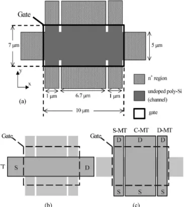
Figure1共a兲illustrates the top view of the test structure. It consists of one test transistor along the x direction关Fig.1共b兲, denoted as TT兴 and three monitor transistors along the y direction 关Fig. 1共c兲, denoted as S-MT, C-MT, and D-MT兴. All TTs and MTs were characterized before and after the stressing. The damage induced at different portions of the channel can be directly characterized by the MTs. It is worth noting that the proposed test structure requires only layout modifications, and could be easily integrated with the display panel processing without extra masks or steps.
Samples in this work were prepared on oxidized Si
wa-a兲Electronic mail: [email protected] FIG. 1. Schematic and operating configurations of the test structure.
0021-8979/2007/101共5兲/054518/5/$23.00 101, 054518-1 © 2007 American Institute of Physics [This article is copyrighted as indicated in the article. Reuse of AIP content is subject to the terms at: http://scitation.aip.org/termsconditions. Downloaded to ] IP:
fers. A 50 nm thick amorphous silicon was deposited and recrystallized at 600 ° C in N2for 24 h, and then patterned to serve as the active device region. Next, a 35 nm thick oxide and 200 nm thick n+poly-Si were deposited and patterned to form the gate dielectric and gate electrode, respectively. Af-terwards, standard processings for source/drain formation, passivation, and metallization were performed. Finally, samples received a plasma treatment in NH3 ambient at 300 ° C for 1 h.
III. RESULTS AND DISCUSSION A. High drain voltage stressing
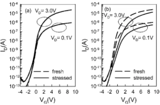
For high drain voltage stressing, the test transistor was stressed under a high VDof 18 V and VGof 9 V. Figures2共a兲
and 2共b兲 show the subthreshold and output characteristics, respectively, of the TT, after 1000 s of stressing. It can be seen that noticeable degradation is observed in the figures. Specifically, a slightly retarded subthreshold swing is ob-served in Fig.2共a兲and a slightly degraded output current in observed in Fig. 2共b兲. These results are consistent with the well-known hot-carrier degradation mechanisms: Hot-carrier stressing can generate additional interface states and/or grain-boundary defect states7 and form a defect-rich and re-sistive region near the drain side.5
The aforementioned damage scenario has been charac-terized in the literature by a number of techniques, including reverse source/drain measurement,8 capacitance-voltage 共C-V兲 measurement,9
device simulation,5,10 asymmetric drain/source structure,8 and picosecond time-resolved emis-sion microscope.11However, all the above methods failed to
directly and unambiguously pinpoint the damage location. By contrast, MTs in our proposed test structure provide use-ful degradation characteristics in different parts of the chan-nel, as shown in Fig.3. It can be seen that the subthreshold characteristics of the MT near the drain side 共D-MT兲 show clear and visible degradations in both subthreshold swing and on-state current共Ion兲. On the contrary, the monitor tran-sistor near the source side 共S-MT兲 depicts only negligible damage. These results confirm that the location dependence of HC degradation could be clearly resolved with the test structure.
B. Low drain voltage stressing
The test structure also provides excellent sensitivity for the detection of hot-carrier degradation. To induce visible degradation, researchers usually resorted to severe stress condition with high stress voltage or sufficiently long stress time. For practical device operation, however, the applied biases to the device are low, so the degradation is almost impossible to observe. The proposed test structure with its high sensitivity is suitable to resolve this problem. This is demonstrated by comparing the characteristics of TT 关Fig.
2共a兲兴 and D-MT 关Fig.3共b兲兴. It is clearly seen that the degra-dation in the normal structure共TT兲 is amplified by the asso-ciated D-MT. To further highlight this feature, the test struc-ture was stressed under VD of 13 V and VG of 6.5 V for
1000 s, a condition where the stress field was much reduced than that in Figs. 2 and 3. As shown in Fig. 4共a兲, the test transistor exhibits barely detectable degradation after the stressing because of the milder stress condition. This will call
FIG. 2. 共a兲 Subthreshold and 共b兲 output characteristics of the test transistor 共TT兲 before and after hot-carrier stress under VG/ VD= 9 V / 18 V for 1000 s.
FIG. 3. Subthreshold characteristics of共a兲 S-MT and 共b兲 D-MT, before and after hot-carrier stress under VG/ VD= 9 V / 18 V for 1000 s.
FIG. 4. Subthreshold characteristics of共a兲 TT and 共b兲 D-MT, before and after hot-carrier stress under VG/ VD= 6.5 V / 13 V for 1000 s.
FIG. 5. Threshold voltage shift of the test structure under various hot-carrier stress conditions with constant VG/ VDratio of 0.5.
054518-2 Lee, Chang, and Lin J. Appl. Phys. 101, 054518共2007兲
for a very long stress time for the TT to produce detectable degradation similar to that shown in Fig. 2. However, the associated D-MT shows visible degradation, as shown in Fig.
4共b兲. The enhanced sensitivity thus allows the study of the degradation under a milder stress condition.
Figures 5 and 6 show the shift in threshold voltage 共⌬Vth兲 and subthreshold swing 共⌬SS兲, respectively, as a function of stress VD with VG= 0.5VD for 1000 s. As
ex-pected, the degradation increases with increasing VD. When
VDis less than 15 V, TTs depict a threshold voltage shift of
less than 100 mV and negligible change in the subthreshold swing. This again indicates that the traditional test structure is not suitable for monitoring milder stress conditions. In contrast, the minor damage can be unambiguously detected with the monitor transistors in the test structure. Moreover, the severely degraded characteristics of D-MTs after stress-ing clearly pinpoint the major damage site. In fact, it is pos-sible to investigate the damage mechanisms in different parts of the channel. This point is further addressed in the follow-ing subsection.
C. Effects of stress gate voltage
Figures7and8 show the shift in threshold voltage and subthreshold swing, respectively, of the TT and MTs after 1000 s stress at VD of 13 V and various VG. It is seen that
⌬Vthof the test transistor is positive in the low VGregime,
monotonically decreases with increasing VG, and becomes
negative as VGexceeds 10 V. The information is, however,
very limited. By contrast, MTs’ data reveal several interest-ing features. First, the drain-side damage is dominant in the low VG regime, and peaks at around VG= 0.5VD. A similar
trend is also observed in ⌬SS, as shown in Fig.8, implying that the generation of oxide interface states and defects at grain boundaries are the likely culprits. The major damage site gradually moves toward the source as VGincreases. The
negative threshold voltage shift in the S-MT device as VG
⬎8 V indicates that hole trapping in the gate oxide now dominates the degradation.
D. Evolution of the HC degradation
From the above results, we can see that the degradation is complicated and is related to both VG and VD. Next, we
investigate the evolution of degradation under two distinctly different stress modes, namely, VG= 0.5VDand VG= VD.
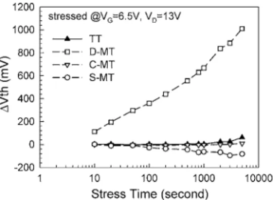
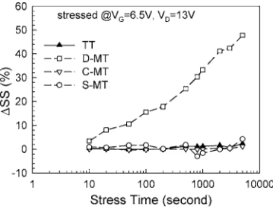
As shown in Figs.9 and10, the evolution of the degra-dation induced in different parts of the channel under
VD/ VG= 13 V / 6.5 V can be directly resolved with the test
structure. Specifically, although TT’s data show negligible subthreshold shift after the stressing, the D-MT shows unam-biguous degradation at a very early stage, and the degrada-tion increases monotonically with increasing stress time. Moreover, a negative threshold voltage shift for S-MTs be-comes clear when the stress time is longer than 100 s. Simi-lar findings can also be found in Figs. 5 and 7, confirming that the dominant damage mechanism is indeed position de-pendent. Although this has been well known in the literature, the direct observation of position-dependent damage
mecha-FIG. 6. Subthreshold swing degradation of the test structure under various hot-carrier stress conditions with constant VG/ VDratio of 0.5.
FIG. 7. Threshold voltage shift of the test structure under various hot-carrier stress conditions at a fixed VDof 13 V.
FIG. 8. Subthreshold swing degradation of the test structure under various hot-carrier stress conditions at a fixed VDof 13 V.
FIG. 9. Evolution of threshold voltage shift of the test structure during hot-carrier stress under VG/ VD= 6.5 V / 13 V.
nisms without involving a complicated experimental scheme illustrates the uniqueness and usefulness of the proposed test structure.
From the aforementioned results, the degradation during HC stressing under VG= 0.5VDcondition is illustrated in Fig.
11. In this case, impact ionization occurs at the drain side by the high field strength, and causes the generation of electron-hole pairs. The generated hot carriers may release their en-ergy in the channel or near the oxide/channel interface where defects are created. Since no substrate contact is present in the TFT structure, the generated holes tend to drift toward the grounded source; some of them may have sufficient en-ergy to surmount the barrier and are injected into the oxide. This mechanism explains the negative threshold voltage shift of S-MTs.
Temporal evolution analyses for devices under VG= VD
stress mode are presented in Figs.12and13. It is seen that the test and all monitor transistors depict a negative threshold voltage shift, implying that the generation of positive charge is mainly responsible for the degradation. Moreover, among these devices, S-MT exhibits the largest shift. It should be noted that, although the S-MT characterized in Fig. 9under
VG= 0.5VD stress mode also exhibits a negative threshold
voltage shift, the extent of the shift in the present case共Fig.
12兲 is much larger. For the two stress modes, it is well known
that the impact ionization rate is suppressed under VG= VD
stress mode.12This indicates that hole trapping illustrated in Fig. 11 alone cannot account for the observation shown in Fig. 12, and some other mechanisms should be responsible for the degradation. It is likely that the oxide field between the gate and the channel plays an important role, as a high gate voltage共e.g., 13 V兲 applied during stressing that exerts an oxide field 共⬃3.7 MV/cm兲 above the channel near the source side. It has been pointed out previously13 that such
field may lead to the generation of a positive charge in the oxide. This phenomenon can consistently explain the results observed in Figs.12and13.
IV. CONCLUSION
In this work, a TFT test structure is employed for the characterization of HC degradation. The fabrication of the proposed test structure is simple and compatible with stan-dard ultra-large-scale integration 共ULSI兲 processing without extra masking. Several advantages of the test structure are demonstrated in this work.共1兲 the capability of resolving the damage characteristics in different parts of the channel, 共2兲 the greatly enhanced sensitivity in detecting the localized damage, which is helpful for studying the damage character-istics under a milder stress condition, 共3兲 the evolution of degradation in specific regions could also be detected di-rectly, and共4兲 dominant damage mechanism could be iden-tified. Specifically, in this work we found that at least two mechanisms are responsible for the negative threshold volt-age shift detected by the monitor transistors. With these unique features, the proposed test structure represents a pow-erful tool in practical applications for studying the reliability of TFT devices.
ACKNOWLEDGMENTS
The authors thank the staff in the National Nano Device Laboratory 共NDL兲 for their help in fabricating the test samples. This work was supported in part by the National Science Council of the Republic of China under Contract
FIG. 10. Evolution of subthreshold swing degradation of the test structure during hot-carrier stress under VG/ VD= 6.5 V / 13 V.
FIG. 11. Schematic illustration of the hot-carrier degradation mechanisms under VG/ VD= 6.5 V / 13 V.
FIG. 12. Evolution of threshold voltage shift of the test structure during hot-carrier stress under VG/ VD= 13 V / 13 V.
FIG. 13. Evolution of subthreshold swing degradation of the test structure during hot-carrier stress under VG/ VD= 13 V / 13 V.
054518-4 Lee, Chang, and Lin J. Appl. Phys. 101, 054518共2007兲
H.-C. Lin, M.-H. Lee, and K.-H. Chang, IEEE Electron Device Lett. 27, 561共2006兲.
共2004兲.
13D. N. Kouvatsos and D. Davazoglou, Thin Solid Films 426, 250共2003兲.