42
4-900784-01-X 2005 Symposium on VLSI Circuits Digest of Technical Papers3-4
A DLL-Based Frequency Multiplier For MBOA-UWB System
Tai-Cheng Lee and Keng-Jan Hsiao
Graduate Institute of Electronics Engineering and Department of Electrical Engineering
National Taiwan University, Taipei, Taiwan
Email: tlee@cc.ee.ntu.edu.tw
A
BSTRACTA delay-locked loop (DLL)–based frequency multiplier is designed for the ultrawideband (UWB) Mode-1 system. This clock generator with 528-MHz input reference frequency can achieve less than 9.5-ns settling time by utilizing wide loop bandwidth and fast-settling architecture. The UWB clock generator has been fabricated in a 0.18-µm CMOS process and consumes only 54 mW from a 1.8-V supply while exhibiting a sideband magnitude of -35.3 dB and -94 dBc/Hz phase noise at the frequency offset of 50 kHz.
Keywords: Delay-locked loops, UWB, frequency multiplier.
I. I
NTRODUCTIONThe UWB system utilizes the unlicensed 3.5-10 GHz band with a strict regulation in emission power less then -41 dBm by FCC. The Multi-Band OFDM Alliance (MBOA) proposed a frequency-hopping spread spectrum (FHSS) communication system, and the frequency plan is shown in Fig. 1. Frequency bands belonging to the group A are for the
Fig. 1. Frequency plan of MBOA-UWB system.
earlier Mode-1 operation whereas the group A and the group C are for the later Mode-2 operation.
The difficulty of generating the desired frequency arises from the stringent restriction on band-hopping time less than 9.5 ns. For the conventional phase-locked loop (PLL)-based frequency synthesizer, it takes hundreds of reference cycles to settle down. In order to settle the loop within 9.5 ns, the reference frequency must be in the order of tens of GHz, thereby obviating this approach. An existing solution implements a non-switching PLL with single-side-band (SSB) mixing to shift the output frequency from the PLL to desired band. However, the SSB mixing has many inherent drawbacks such as high phase noise, high power, and spurious tones. The LO leakage and the unwanted sideband translate adjacent interferences to the baseband and corrupt the signal at the desired channel. All foregoing non-ideal effects degrade the performance of the UWB transceivers severely.
To overcome these problems, a DLL-based frequency multiplier is proposed in this paper. DLLs outperforms PLL in phase noise because the later accumulates the jitter over hundreds of reference cycles before being removed. Additionally, the DLL can be designed as a first-order system to allow wider loop bandwidth and settle down within 9.5 ns.
Section II describes the architecture of the system. Circuit details, including the design of the delay cell, high-speed phase frequency detector (PFD) as well as charge pump (CP) circuits are described in Section III. Experimental results are presented in Section IV.
II. C
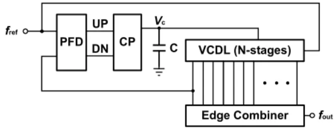
LOCK GENERATOR ARCHITECTUREThe DLL-based frequency multiplier consists of a DLL and an edge combiner (EC), illustrated in Fig. 2. Delay cells
Fig. 2. DLL-based frequency multiplier.
in the N-stage voltage-controlled delay line (VCDL) generate
N equal phase-spaced clocks, and the phase shifted clocks
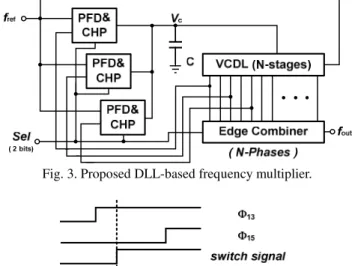
are combined together by an edge combiner to produce the multiple of the input reference frequency. The conventional technique [1][2] can only generate a single output frequency for a fixed reference frequency, whereas the UWB system demands three carrier frequencies. A modified DLL-based frequency multiplier shown in Fig. 3 can change the multiplication factor of the reference frequency. By switching the feedback clock from one delay cell to another, the equivalent number of delay cells is changed, and the output frequency will hop to a different band consequently because the multiplying factor is equal to the number of delay cells. Because the loop bandwidth of the DLL is relatively large, any undesired glitch resulting from the switching between different clocks slows the settling time severely. This switching problem can be alleviated by using three PFDs & CHPs shown in Fig. 3. To determine the
43
2005 Symposium on VLSI Circuits Digest of Technical Papersnumber of delay cells, we decompose the carrier frequencies as listed in Table I.
Fig. 3. Proposed DLL-based frequency multiplier.
Fig. 4. An undesired glitch (switching fromΦ13toΦ15).
Therefore, the numbers of delay cells are 13, 15, and 17, respectively. However, the loop bandwidth of the DLL is directly constrained by the frequency of the reference clock,
Table I. Frequency decomposition.
and a reference clock of 264 MHz cannot guarantee sufficient loop bandwidth. 528 MHz, two times of 264 MHz, is chosen as the input reference clock and consequently, the output of the edge combiner must be divided by 2 to obtain the desired carrier frequencies. The great benefit is this clock generator can produce quadrature clocks, essential for any digital quadrature modulation.
The loop bandwidth of the DLL equals to , L VCDL ref CP n C K f I ⋅ ⋅ = ω (1)
where fref is the reference frequency, Icp is the charge pump
current, CL is the loop filter capacitor, and KVCDL is the
VCDL gain ( s/V ). The loop bandwidth of the DLL must be designed wide enough such that the DLL can settle down within 9.5 ns. In this work, the bandwidth of DLL is chosen to be approximately 160 MHz for fast settling.
When the DLL is locked, each of the delay cells shifts the phase of the reference clocks by 2π/N (rads). Figure 5 shows
that each output signal coming from a delay cell is represented by a vector for N=5. Each signal from the delay cell is evenly phase-spaced, and all of higher order harmonic tones can be suppressed except the N-th harmonic tone. The frequency of the output signal is therefore multiplied by N times. Nevertheless, the random mismatches of N delay cells drive the actual phase of the delayed clock to deviate from the ideal phase. The phase error between the actual and the ideal phase can be approximated as in Fig. 6. For a small
Fig. 5. The vector diagram for N equal phase-spaced signals.
Fig. 6. The approximation of phase error.
phase error, the amplitude of the erroneous phase can be expressed as , / k A Ak = ref (2) . err k err k A A = ⋅ ⋅
θ
(3)In (2), Ak is the amplitude of the kth harmonic, and Aref
represents the amplitude of the reference clock. Equation (3) indicates that the erroneous amplitude (Aerr) for the kth
harmonic due to phase error (θerr) is equal to k times A θerr..
Therefore, for a fixedθerr, the signal-to-distortion ratio of the
output of the edge combiner is independent of the multiplication factor (N). Additionally, because the ideal phase and erroneous phase in Fig. 6 are orthogonal to each other, the erroneous phases are equally phase-spaced. Therefore, they will be partially cancelled out, reducing the magnitude of the spurs. System simulations show that delay cells with 1% phase error only induce -40 dBc spurious tones.
III.
B
UILDING BLOCKSA. Delay Cell
In Fig. 7, the delay cell [2][3] comprises of a single-ended inverter (M2and M3) with series transistors M1and M4
Fig. 7. Current-starving delay cell.
operating in the triode region. The delay of this circuit is determined by the equivalent resistance of M1 and M4,
controlled by Vc and Vcp, controlled by the driving circuits
M7and M8. An inverter inserted between delay cores serves
as an output buffer. Because the circuit can perform rail-to-rail operation, it consumes no DC power.
Carrier
Frequency Decomposition 3432 MHz 264 X 13 MHz 3960 MHz 264 X 15 MHz 4488 MHz 264 X 17 MHz
44
4-900784-01-X 2005 Symposium on VLSI Circuits Digest of Technical Papers Nevertheless, the differential signals are preferable forcommon-mode rejection. Figure 8 shows that cross-coupled inverters are utilized to regulate the differential output to perform pseudo-differential operation.
Fig. 8. Pseudo-differential delay cell.
B. Edge Combiner
The edge combiner synthesizes desired output frequency based on the multiple-phase outputs of the DLL. Shown in Fig. 9, the differential pairs convert voltage signals to current signals and sum up at the output node. The output load comprises of a variable LC-tank to tune the center frequency of the tank by the switched-capacitor array. Due to 1.5-GHz wideband operation, variable tank frequency is required to maintain output signal power for all three bands. The quality factor of the tank is less important in this edge combiner, because the phase noise is dominated by the noise in the input reference clock rather than by the Q of the inductor. The quality factor of the inductor is chosen to be 10 here to achieve adequate output swing with a reasonable current consumption.
Fig. 9. Edge combiner with tunable load.
C. Divided-by-2 Circuit
A divided-by-2 divider takes the output from the edge combiner and generates quadrature outputs. A static divided-by-2 divider, shown in Fig. 10, is used in this work to generate all three frequencies. Operating at the frequency up to 9 GHz, current-mode logic (CML) is used in this divider.
D. PFD & CHP
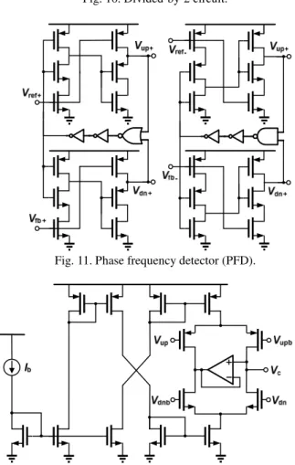
To enhance common-mode rejection, a pseudo-differential dynamic phase frequency detector (PFD) [4], shown in
Fig. 11, compares the phase of the reference clock with the feedback clock. A differential charge pump is realized for the high-speed operation, shown in Fig. 12. The differential UP and DOWN control signals are produced by a pair of complementary PFDs shown in Fig. 11. The effect of charge sharing is removed by the unity-gain feedback amplifier in the charge pump, and the static phase error is reduced consequently.
Fig. 10. Divided-by-2 circuit.
Fig. 11. Phase frequency detector (PFD).
45
2005 Symposium on VLSI Circuits Digest of Technical PapersIV
.E
XPERIMENTAL RESULTSThe DLL-based UWB clock generator has been fabricated in a 0.18-µm CMOS technology. Figure 13 is a photograph of the die, whose area is 0.98 mm by 0.8 mm.
Fig. 13. Die photo.
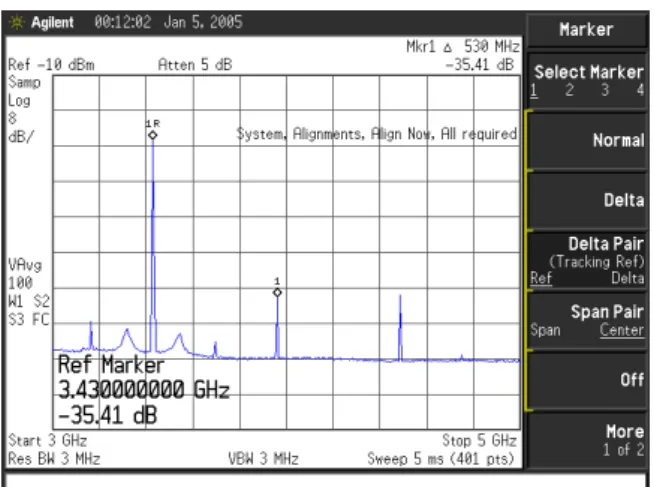
The circuit has been tested by a chip-on-board assembly while running at the input frequency of 528 MHz from a 1.8-V power supply. Figure 14 shows the output spectrum of
Fig. 14. Output spectrum at 3432 MHz.
the clock generator for the carrier frequency at 3432 MHz. The adjacent channel spur suppression is about -35.4 dB. Figure 15 shows the output spectrum at 3960 MHz with 1 MHz frequency span. The phase noise of the clock generator is also measured. The phase noise is measured as -94 dBc/Hz at the frequency offset 50 kHz.
The switching time of this clock generator is measured at the sampling scope. The channel control signal is toggled by a 6-MHz pulse. Figure 16 shows that the clock generator can switch between two adjacent channels within 8 ns. Table II summarizes the performance of this clock generator.
ACKNOWLEDGMENT
This work was supported by National Science Council under contract 93-2220-E-002-017. The author would like to thank the support of Mediatek for chip fabrication.
Fig. 15. Output spectrum at 3960 MHz.
Fig. 16. Settling behavior between two adjacent channels.
Carrier Frequency 3432 MHz 3960 MHz 4488 MHz Phase Noise -94 dBc/Hz at 50 kHz offset Settling Time 8 ns
Power Dissipation 54 mW Supply Voltage 1.8 V Die Area 0.98 mm x 0.8 mm Technology 0.18-µµµµm CMOS
Table II. Performance Summary. REFERENCES
[1] G. Chien and P. R. Gray, “A 900-MHz Local Oscillator Using a DLL-Based Frequency Multiplier Technique for PCS Applications,” IEEE J. Solid-State Circuits, vol. 35, pp. 1996-1999, Dec. 2000.
[2] J. Zhuang, Q. Du and Tad Kwasniewski, “A -107dBc, 10kHz Carrier Offset 2-GHz DLL-Based Frequency Synthesizer,” Proc. of Custom Integrated Circuits Conf., 2003, pp. 301-304.
[3] R. Farjad-Rad, W. Dally, H.-T. Ng, A. Senthinathan, M.-J. Lee, R. Rathi and J. Poulton, "A Low-Power Multiplying DLL for Low-Jitter Multigigahertz Clock Generation in Highly Integrated Digital Chips," IEEE J. Solid-State Circuits, vol. 37, pp. 1804-1812, Dec. 2002.
[4] S. Kim, K. Lee, Y. Moon, D.-K. Jeong, Y. Choi and H. K. Lim, "A 960-Mb/s/pin Interface for Skew-Tolerant Bus Using Low Jitter PLL," IEEE J. Solid-State Circuits, vol. 32, pp. 691-700, May 1997.