J O U R N A L O F M A T E R I A L S S C I E N C E 3 4 (1 9 9 9 ) 4573 – 4578
Optical and structural properties of (Ba, Sr)TiO
3
thin films grown by radio-frequency
magnetron sputtering
Y. P. WANG, T. Y. TSENG
Department of Electronic Engineering and Institute of Electronics, National Chiao-Tung University, Hsinchu, Taiwan, Republic of China
E-mail: [email protected]
We studied the structural and optical properties of (Ba, Sr)TiO3(BST) films deposited on the
transparent substrates at various temperatures of 350–650◦C and annealed at 450–650◦C. Improved crystallization can be observed on 650◦C annealed film whose substrate
temperature is 350◦C. The refractive index increased from 2.17 to 2.59 atλ = 410 nm for the BST films deposited at 350–650◦C and it varied from 2.17 to 2.25 after annealing up to 650◦C. In addition, the refractive-index dispersion data related to the short-range-order structure of BST films obeyed the single-oscillation energy model. The indirect energy gap of the films deposited on Al2O3and quartz substrates was found to be about 3.5 eV.
According to the analysis of reflectance data, the optical inhomogeneity of films can be reduced by depositing the films at intermediate temperatures 450–550◦C. °C 1999 Kluwer Academic Publishers
1. Introduction
At present, ferroelectric thin films have received much attention for fabricating novel functional devices [1–6]. In particular, the ferroelectric films are expected to be excellent in realization of various optical-applications due to their wide energy gap (>3 eV), large static di-electric constant, high refractive index and low absorp-tion coefficient. The optical properties of the epitaxial PLT thin films grown on MgO and Al2O3 substrates
have been investigated [7]. Zhu et al. [8] studied the film-size effect on the optical energy gap of BaTiO3.
The (Ba, Sr)TiO3(BST) films, conrast to above
men-tioned ferroelectric materials, can display paraeletric phase by controlling Ba/Sr ratio and perform a high transparency as an insulating layer of an electrolumi-nescent devices [9]. The current research on the optical properties of BST should attract more interests due to its potential applications in flat panel displays and in-tegrated optics.
In this study, the BST thin films were prepared on the transparent substrates by rf-sputtered at substrate temperatures 350–650◦C. We investigated the effect of substrate temperature on the structure and optical prop-erties of BST films. On the basis of single-oscillator model [10], the parameters related to the short-range-order structure were analyzed.
2. Experimental
BST films were sputtered on the clean Corning 7059 glass, fused-quartz and (1¯102)-oriented Al2O3 by a
magnetron radio-frequency sputtering system. The
(Ba0.7Sr0.3)TiO3target of 2 in. diameter and 0.125 in.
thickness was fabricated using standard solid-state pro-cess. An operating pressure of 40 mTorr was main-tained by a mixture of high-purity argon and oxygen at a flow ratio of 20/1. All films were deposited at a fixed radio-frequency power of 80 W for 2.5 h and the sub-strate temperature was varied from 350 to 650◦C using a quartz halogen lamp. Post-annealing of the 350◦ C-deposited film was carried-out in an argon atmosphere for 2 h at temperatures ranging from 450 to 650◦C. The film crystal structures were examined using X-ray diffraction (XRD, Siemens D5000) with CuKα radia-tion. The optical transmittance and reflectance of BST films were measured in the wavelength range of 250– 900 nm using double beam spectrophotometer (Hitachi model U3410 UV-Vis-NIR). The optical constant and film thickness were calculated on the basis of the enve-lope technique and interference-fringe equation [11]. The film thickness was also cross-checked from the fracture surface of the film by scanning electron micro-scope (SEM, Hitachi, S-4000).
3. Results and discussion
Fig. 1a displays XRD patterns of the films deposited on Corning substrates at various substrate tempera-tures ranging from 350 to 650◦C. The intensities of (100), (110) and (200) peaks were enhanced with the increasing substrate temperature, indicating that better crystallinity can be obtained at higher substrate tem-peratures. Fig. 1b revealed that the crystallization of 350◦C-deposited film can be improved by subsequent annealing at 650◦C.
Figure 1 (a) XRD patterns of BST films deposited on Corning substrates
at various substrates temperatures indicated (b) XRD patterns of BST films deposited on Corning substrates at 350◦C (i) and followed by annealing at 650◦C (ii).
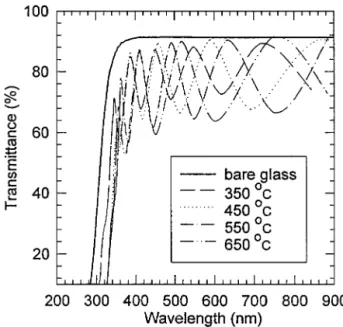
Fig. 2 depicts the spectral transmittance characteris-tic of bare Corning substrate and the BST films deposit-ed on it at various substrate temperatures. The interfer-ence fringes are a result of the interferinterfer-ence between the air-film and film-substrate interfaces. The refrac-tive index (n) was derived by employing the envelope method [11] on the basis of the following expressions:
n= h N+¡N2− n2s¢1/2 i1/2 (1) N = 2ns µ 1 Tmin − 1 Tmax ¶ + n2s + 1 2 (2)
in which Tmaxand Tminare the corresponding
transmit-tance maximum and minimum at a certain wavelength
λ, one being measured and the other calculated; ns is
the refractive index of Corning glass substrate (≈1.51). Fig. 3 displays the calculated refractive index (n) as a function of wavelength (λ) for various substrate
tem-Figure 2 Transmittance spectra as a function of wavelength for BST
films deposited at various substrate temperatures.
Figure 3 Variation of refractive index as a function of wavelength
de-posited at various substrate temperatures for 2.5 h.
peratures. The refractive index increased from 2.17 to 2.59 (atλ = 410 nm) as temperature increased from 350 to 650◦C. The behavior of n vs.λ can be fitted into a formula [11], n= A + Bλ+λC2, as shown by solid lines
in Fig. 3. The dependence of n on substrate temper-ature was consistent with those normally observed in many oxides [12–15]. The increase of the refractive in-dex of the films deposited at higher temperature may be attributed to an increase in packing density, crystal-lization and also to the oxygen deficiency [12–15].
Figure 4 (a) Transmittance spectra as a function of wavelength for the
as-deposited (=350◦C) and subsequently annealed BST films. (b) Vari-ation of refractive index as a function of wavelength for the as-deposited and annealed BST films.
Fig. 4a depicts no significant change in transmit-tance maxima and minima for the films annealed at lower temperatures whereas transmittance maxima and minima decreased and the interference pattern shift toward a longer wavelength region in the 650◦C an-nealed film. Fig. 4b shows the variation of refractive index as a function of wavelength for the film de-posited at 350◦C and subsequently annealed at 650◦C. The lower transmittance after 650◦C annealing may be mainly due to the strong scattering of the light in the film caused by some discernible microcracks arising from mismatched thermal expansion of the film and substrate. Suhail et al. [12] found that the TiO2film deposited at room temperature, after
anneal-ing at 700◦C, showed an increased refractive index, (1n/n) = +7.3% at 550 nm, a thickness reduction of
−20% and a shift in the spectral pattern to a lower
wave-length region (1λm/λm< 0) resulting from the effect
of interference fringe, 2nd= mλ. Our result for the
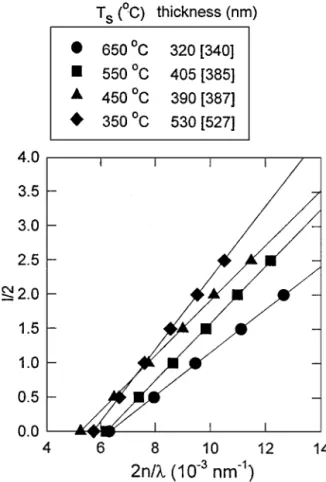
an-Figure 5 Plot of (m/2) vs. (2n/λ) for the BST films deposited at
var-ious substrate temperatures to obtain film thickness. The number in ( ) represents the thickness observed by SEM.
nealing of BST film with1n/n = +3.9% at λ = 550 nm and1λm/λm> 0 revealed a lesser thickness reduction
after annealing at 650◦C.
Fig. 5 indicates the least-square fit of the measured re-fractive index vs. wavelength by the interference-fringe relation [11], m 2 = d µ 2n λ ¶ − k, m = 0, 1, 2, . . . (3)
in which k is the order number of the observable first ex-treme (m= 0) of the spectrum. The film thickness can be obtained from the slope of the plot shown in Fig. 5. These thickness is in good agreement with those (num-bers indicated in [ ] of Fig. 5), which were observed by SEM.
According to the single-oscillation model [10], the refractive index as a function of wavelength can be ex-pressed as: n2− 1 = EoEd E2 o− ¡hc λ ¢2 (4)
where c is the light speed, h Planck constant, Eothe
single-oscillator energy and Edthe dispersion energy.
The Eoand Edvalues can be obtained from the intercept
and slope of the plot (n2− 1)−1 vs.λ−2, respectively.
Fig. 6 exhibits a sufficient extended region of linearity which can be employed to determine Eoand Ed. At long
T A B L E I The fitting parameters obtained from the single-oscillation model for BST films deposited at various substrate temperatures
Substrate Dispersion Empirical
temperature Single oscillation energy ratio
Ts(◦C) energy Eo(eV) Ed(eV) β (eV)
350 6.89 20.61 0.214
450 6.69 26.14 0.272
550 6.42 26.33 0.274
650 5.87 24.48 0.255
Figure 6 Plots of refractive-index factor (n2− 1)−1vs.λ−2for the BST films deposited at various substrate temperatures.
wavelengths region, a curvature deviation from lin-earity is usually observed due to negative contribu-tion of lattice vibracontribu-tions to the refractive index [10]. The corresponding Eo, as summarized in Table I,
de-creases with increasing substrate temperature whereas Ed(=24.48 eV) at higher substrate temperature 650◦C
is close to the Edof pure bulk BaTiO3(Ed= 23.3 eV)
and SrTiO3(Ed= 23.32 eV) materials [10]. Structure
should play an influential role for oscillation and disper-sion energies. For lower temperature deposited films, a small amount of amorphous phase would result in higher Eo value. Table I also includes the values of β = Ed/(NcZaNe) [10], where Nc (=6) is the
coordi-nate number of cation nearest neighbor to the anion, Za(=2) the chemical valency of the anion and Ne(=8)
the effective number of valence electrons per anion. The observedβ values in our cases are coincident with the empirical values given by β ≈ 0.26 ± 0.04 eV, which was followed by many bulk oxides [10].
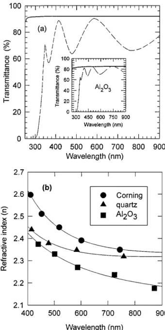
Fig. 7a displays the transmittance spectra of BST films deposited on Al2O3(ns= 1.80) and fused-quartz
(ns= 1.51) substrates. The low-wavelength absorption
of bare Al2O3and quartz substrates is much weaker than
that of bare corning substrate. Their refractive index as a function of wavelength is shown in Fig. 7b. The low-wavelength absorption data for BST films prepared on Al2O3and quartz substrates is related to the
fundamen-tal absorption which refers to the band-to-band
transi-Figure 7 (a) The transmittance spectra of bare quartz substrate and
650◦C. The insert plot displayed transmittance spectra of bare Al2O3 substrate and BST films deposited on it, and (b) Variation of refractive index as a function of wavelength for BST films prepared on various substrates.
tion, i.e., to the excitation of an electron from the va-lence band to the conduction band. The BST energy gap can be obtained from the following equations [16, 17]:
αhν = constant × (hν − Eg)2 (5)
where hν is the photon energy, Egthe optical energy gap
of allowed indirect and direct transition. The absorption coefficient,α is given as [17] α = ln ¡1 T ¢ d (6)
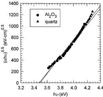
in which T the transmittance and d the film thickness. The (αhν)1/2vs. hν plots for the films on Al2O3and
quartz substrates as represented by Equation 5 show good linearity at wavelength below 400 nm, as shown in Fig. 8. The plots of (αhν)1/2vs. hν were found not to
Figure 8 Plot of (αhν)1/2vs. hν for BST films deposited on Al2O3and
fused quartz substrates.
thus supporting the model of indirect band gap for the deposited films. By extrapolating the linear portion of these curves to zero absorption, the calculated energy gaps were about 3.5 eV which are close to the energy gaps of BaTiO3films (3.6–4.1 eV) [8, 18] and SrTiO3
ceramic (=3.43 eV) [19]. The reduced energy gap of (Ba, Sr)TiO3might be due to the Sr in the Ba site
sub-stitution.
The optical inhomogeneity of the films was analyzed by using the near normal reflectance of the films and the bared substrate surface. The inhomogeneous refractive index (1n) along the film thickness was determined using the empirical relation [20]:
1n = no− ni= nav
Rf− Rs
4.4Rs
(7) The noin Equation 7 is the refractive index at the
air-film interface, niat the film-substrate interface and nav
the average index of the film. Rs and Rf are the
re-flectance at the front surface of the substrate and films, respectively. Both Rs and Rf can be computed from
the measured reflectance of the bare and deposited substrate, Rso and Rfo, using the following
expres-sions [21]: Rso= 2Rs 1+ Rs (8) Rfo= Rf+ Rs(1− Rf)2 (1− RsRf) (9) where1n can be positive or negative according to the gradation in the film [20]. Negative1n value indicates that the refractive index decreases from substrate to the top surface of the film and vice versa. The degree of inhomogeneity of the films,1n/nav, calculated from
the points of reflectance minima around 600–700 nm, where the Rso(Rs) is almost independent ofλ, as shown
in Fig. 9 and Table II, was found to vary from −7.3 to −4.3% as the substrate temperature was increased
T A B L E I I Optical inhomogeneity analysis for the films deposited at various temperatures Substrate Wavelength 1n/nav temperature (◦C) (nm) (%) 350 715 −7.3 450 593 −3.3 550 630 −3.7 650 739 −4.3
Figure 9 Observed reflectance spectra as a function of wavelength for
bare substrate (Rso) and BST films (Rfo) deposited at various substrate temperatures.
from 350 to 650◦C. The optical homogeneity of BST films was found to be better for the films deposited at intermediate temperatures 450–550◦C.
4. Conclusions
We have studied the effect of various substrate tempera-tures as well as post annealing on the structural and op-tical properties of BST films prepared by rf magnetron sputtering. Crystallization sets in at the deposited films and it is further improved by post-deposition anneal-ing at 650◦C, as observed from X-ray results. The refractive index of the films were increased with an in-creased substrate temperature. The film thickness cal-culated from interference-fringe equation is in good agreement with the one observed by scanning electron microscope. The dependence of refractive index on the wavelength obeys the single-oscillation model, from which the parameters Eo, Edandβ were determined
and were consistent with the experimental values for most oxides. The energy gap of the deposited films on various substrates was found to be around 3.5 eV of indirect-transition type. The film deposited at 350◦C was more inhomogeneous whereas it has better optical homogeneity when deposited at intermediate substrate temperature.
Acknowledgement
This work was support from the National Science Coun-cil of Republic of China under project no. NSC 86-2112-M009-028. References 1. T.M A T S U K I,Y. H A Y A S H IandT.K U N I O, IEDM-95 (1996) 691. 2. M. H. S O N G,Y. H. L E E,T. S. H A N NandM. H. O H, J. Appl. Phys. 79 (1996) 3744.
3. K. O K A M O T O,Y.N A S UandY.H A M A K A W A, IEEE Trans.
Electron Devices ED-28 (1991) 698.
4. A. Y U U K I, M. Y A M A M U K A, T. M A K I T A, T. H O R I K A W A,T. S H I B A N O,N. H I R A N O,H. M A E D A,N. M I K A M I,K. O N O,H. O G A T AandH. A B E, IEEE IEDM-95 (1995) 115.
5. Y. P. W A N GandT.Y. T S E N G, J. Appl. Phys. 81 (1997) 6762. 6. A. K I N G O N,S. K. S T R E I F F E R,C. B A S C E R IandS. R.
S U M M E R F E L T, MRS Bulletin (1996) 46.
7. Y. K I MandA. E R B I L, Appl. Phys. Lett. 70 (1997) 143. 8. J. S. Z H U,X. M. L U,W. J I A N G,W. T I A N,M. Z H U,
M. S. Z H A N G,X. B. C H E N,X. L I UandY. N. W A N G, J.
Appl. Phys. 81 (1997) 1392.
9. T. S. K I M,M. H. O HandC. H. K I M, Jpn. J. Appl. Phys. 32 (1993) 2837.
10. S.H. W E M P L EandM. D I D O M E N I C O, Phys. Rev. B 3 (1971) 1338.
11. R. S W A N E P O E L, J. Phys. E, Sci. Instrum. 16 (1983) 1214. 12. M. H. S U H A I L,G. M. R A OandS. M O H A N, J. Appl. Phys.
71 (1992) 1421.
13. M. G. K R I S H N A,K. N. R A O,M. A. M U R T H Y andS. M O H A N, J. Mater. Sci. Eng. B 5 (1990) 427.
14. M.M E S B A H,A. B O Y E RandE.G R O U B E R T, ibid. 27 (1992) 83.
15. H. K U S T E RandJ. E B E R T, Thin Solid Films 70 (1980) 43. 16. S. R. E L L I O T T, “Physics of Amorphous Materials” (John Wiley
& Sons, New York, 1990) p. 328.
17. E. A. D A V I SandN. F. M O T T, Phil. Mag. 22 (1970) 903. 18. A. M A N S I N G HandC. V. R. V A S A N T A, J. Mater. Sci. Lett.
7 (1988) 1104. 19. M. N. K A M A L A S A N A N, N. D. K U M A R and S. C H A N D R A, J. Appl. Phys. 74 (1993) 679. 20. D. P. A R N D T,R. M. A Z Z A M,J. M. B E N N E T T,J. P. B O R G O N O, C. K. C A R N U G L I A,W. E. C A S E, J. A. D O B R O W O L S K I,U. J. G I B S O N,T. T. H A R T,F. C. H O,V. A. H O D G I N,W. R. K L A P P,H. A. M A C L E O D, E. P E L L E T I E R,M. K. P U R V I S,D. M. Q U I N N,D. H. S T O M E,R. S W E N S O N,P. A.T E M P L EandT. F. T H O U N, Appl. Opt. 23 (1984) 3571. 21. R. J A C O B S S O N, Arkiv Fys. 24 (1963) 17. Received 24 November 1997 and accepted 10 March 1999