IEEE ELECTRON DEVICE LETTERS, VOL. 35, NO. 6, JUNE 2014 651
On the Origin of Anomalous Off-Current Under
Hot Carrier Stress in p-Channel DDDMOS
Transistors With STI Structure
Ching-En Chen, Ting-Chang Chang, Senior Member, IEEE, Hua-Mao Chen, Bo You,
Kai-Hsiang Yang, Szu-Han Ho, Jyun-Yu Tsai, Kuan-Ju Liu, Ying-Hsin Lu,
Yu-Ju Hung, Ya-Hsiang Tai, and Tseung-Yuen Tseng
Abstract— This letter investigates the abnormal OFF-current behavior induced by hot carrier stress (HCS) in p-channel double diffused drain metal-oxide-semiconductor transistors with a shallow trench isolation (STI) structure. According to ISE-TCAD simulation, the electric field at the drain-side corners of the high-voltage n-well (HVNW) adjacent to the STI trench is stronger than the electric field in the channel center in width direction. Moreover, because a nitride layer acts as a buffer in STI, the electrons generated by impact ionization at the corners of the HVNW can be easily trapped in the nitride layer or at the liner oxide/nitride layer interface. Furthermore, the extension of electron trapping in STI from drain to source during HCS forms the OFF-current conductive path. Based on the charge pumping measurements at different operation conditions, this path for-mation is further demonstrated by the comparisons of charge pumping measurements between initial state and after HCS.
Index Terms— Hot carrier stress, double diffused drain
metal-oxide-semiconductor (DDDMOS), shallow trench isolation (STI).
I. INTRODUCTION
R
ECENT applications of mobile electronic products have combined display designs [1]–[3], memory [4]–[6] and IC circuits. To accomplish high power efficiency and reduce chip size in IC circuits, high-voltage (HV) devices suchManuscript received March 18, 2014; accepted April 5, 2014. Date of publication April 24, 2014; date of current version May 20, 2014. This work was supported in part by the National Science Council Core Facilities Laboratory, Nano-Science and Nano-Technology, Kaohsiung-Pingtung, in part by the Center for Nanoscience and Nanotechnology, National Sun Yat-Sen University, and in part by the National Science Council of Taiwan under Contract NSC-102-2120-M-110-001. The review of this letter was arranged by Editor S.-H. Ryu.
C.-E. Chen, S.-H. Ho, and T.-Y. Tseng are with the Department of Elec-tronics Engineering, National Chiao Tung University, Hsinchu 300, Taiwan.
T.-C. Chang is with the Department of Physics, National Sun Yat-Sen University, Kaohsiung 804, Taiwan, the Advanced Optoelectronic Technol-ogy Center, National Cheng Kung University, Tainan 701, Taiwan, and also with the Department of Photonics, National Sun Yat-Sen University, Kaohsiung 804, Taiwan (e-mail: tcchang@mail.phys.nsysu.edu.tw).
H.-M. Chen and Y.-H. Tai are with the Department of Photonics, Institute of Electro-Optical Engineering, National Chiao Tung University, Hsinchu 300, Taiwan.
B. You and Y.-J. Hung are with the Department of Photonics, National Sun Yat-Sen University, Kaohsiung 804, Taiwan.
K.-H. Yang is with the Department of Electrical and Computer Engineering, University of Toronto, Toronto, ON M5S 3G4, Canada
J.-Y. Tsai, K.-J. Liu, and Y.-H. Lu are with the Department of Physics, National Sun Yat-Sen University, Kaohsiung 804, Taiwan.
Color versions of one or more of the figures in this letter are available online at http://ieeexplore.ieee.org.
Digital Object Identifier 10.1109/LED.2014.2316316
as lateral diffused metal-oxide-semiconductor (LDMOS) and double diffused drain MOS (DDDMOS) technology have been developed in the manufacturing process. Furthermore, because such HV devices are operated at high drain and gate biases, hot carrier reliability has become a serious issue. Although width-dependent hot-carrier degradation for p-channel MOS devices has been reported in some previous studies [7]–[9], there are few reports that study the off-current behavior for p-channel DDDMOS after hot carrier stress (HCS). Therefore, in this work, the mechanism of anomalous off-current in p-channel DDDMOS transistors with a shallow trench isola-tion (STI) structure under HCS has been investigated.
II. EXPERIMENT
The p-channel DDDMOS transistors used in this study were fabricated with 0.15 µm CMOS fabrication and featured a double diffuse drain region. In the STI process flow, after the trench formation, the silicon surface of the trench is oxidized and is followed by a deposition of a thin nitride layer, then the STI oxide. After that is a CMP treatment. In this letter, the device has dimensions of width/length= 20 µm/1.1 µm. The I-V characteristics were performed by an Agilent B1500A semiconductor device analyzer and Cascade Microtech M150 measurement platform.
III. RESULT ANDDISCUSSION
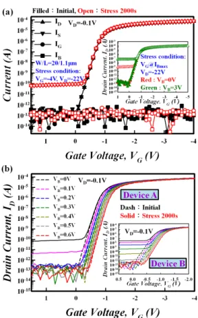
Fig. 1(a) shows the current comparisons between the I-V characteristics at the initial state and after HCS of 2000 s with VG = −4 V, VD = −22 V, and source and body
grounded (IBmax stress). After stress, both drain current (ID) and source current significantly increase in the off region (VG > 0V) and cause a high off-current. Furthermore, the contributions of gate and body currents are negligible after HCS. This apparent result shows that the high off-current is a source to drain current through the high-voltage n-well (HVNW). The inset of Fig. 1(a) shows the comparison of ID-VG at the initial state and after IBmax stress with VB= 0V
(device A, IBmax = 35.54 µA) and VB = 3V (device B,
IBmax = 32.76 µA). Obviously, the off-current after stress
in device B is larger than that in device A. However, the IBmax shows the contrary result in the comparison between
device A and device B. It means that the electric field in the
0741-3106 © 2014 IEEE. Personal use is permitted, but republication/redistribution requires IEEE permission. See http://www.ieee.org/publications_standards/publications/rights/index.html for more information.
652 IEEE ELECTRON DEVICE LETTERS, VOL. 35, NO. 6, JUNE 2014
Fig. 1. (a) Current comparisons between the I-V characteristics at initial state and after HCS of 2000 s with VG= −4 V, VD= −22 V, and source
and body grounded (IB,max). The inset shows the comparison of ID-VGat the
initial state and after IBmaxstress with VB= 0V (device A) and VB= 3V
(device B). (b) The application of reverse body bias can reduce the off-current and increase the threshold voltage in device A and device B.
depletion region of the HVNW/PDDD (drain side) junction where below the path for the main current (ED,BULK) is the
other important factor for the off-current. From the Fig. 1(a), the threshold voltage (Vth) and the subthreshold swing (S.S)
almost unchanged after HCS. It means that there is negligible degradation in the gate oxide where the overlap between gate oxide and HVNW. In addition, the body current increases with VD(not VGD) in the off region after HCS because the
junction degradation at drain side (IB-VG curves in the off
region with different VD can demonstrate this, but are not
shown here).
To further study the origin of the off-current after HCS, Fig. 2(a) shows the top view and an enlargement of the STI edge at the drain side to illustrate the degradation mechanism during HCS. Under HCS, the electric field at the drain-side corners on the STI trench edge is larger than that in center of the channel in width direction. This behavior is confirmed by the electric field distribution in the ISE-TCAD simulation shown in Fig. 2(b). Because of the strong electric field at the drain-side corners in the path for main current (ED,SUR.), the
other one below the path for the main current (ED,BULK), and
the nitride layer in STI, the electrons generated by impact ionization (I.I.) at the drain-side corners can be accelerated by ED,BULK into the deep region of HVNW and then these
hot electrons can be easily trapped in the nitride layer, or at
Fig. 2. (a) Schematic of top view and its enlargement of STI edge at drain side to illustrate the degradation mechanism during HCS. (b) ISE-TCAD simulation for electric field distribution below gate oxide/Si interface during HCS at drain side. (c) The cross-section in the width direction illustrating the main and off-currents in the device after HCS.
the liner oxide/nitride layer interface. However, the absence of hole trapping can be due to the higher barrier height for hole trapping, the shorter mean free path, the larger effective mass and the larger voltage across gate to drain [10], [11]. Furthermore, the enlargement in Fig. 2(a) shows the sequence of electron trapping in STI during HCS. In the beginning of HCS, the electron trapping in STI occurs near the drain side, with subsequent electron trapping progressively toward the source side because the lateral electric field direction at drain side is toward the source side and because trapping occurs at the next unoccupied location along the STI edge. And then this trapping will be stopped at the region where it is adjacent to the depletion region in HVNW at source side because of the direction of the electric field. As a result, the conductive path for off-current is formed as shown in Fig. 2(a). Fig. 2(c) shows the cross-section in the width direction. After HCS, the conductive path for off-current at the STI edge below the main current can be formed due to the fact that the electrons are trapped in STI. In addition, from the variations of Vth and
S.S after HCS and the effect of ED,BULKon off-current, this
position of the off-current has been concluded that it is beyond the maximum depletion region because of the surface potential of main current is not affected after HCS.
As was shown in Fig. 1(b), the off-current can be influenced by VGand VB; the VGand VBdependencies on off-current are
illustrated by the energy band diagrams of the channel shown in Fig. 3. After HCS, there are two channels in the device: the one for the main current is called the surface channel, and the other for off-current is called the parasitic channel. When VG = 0 V and VB= 0 V, the main current is turned-off,
shown in Fig. 3(a). However, the off-current still exists due to the electron trapping in STI which reduces the barrier height between PDDD at the source side and HVNW surface at the STI edge. In Fig. 3(b), as VG increases to state, the
off-current slightly decreases (as can be seen in Fig. 1(b)) because this current is below the main current and the influence of VG
on this current is limited. However, the energy bands of the HVNW surface of the surface and parasitic channels will be reduced dramatically by applying reverse VB as in Fig. 3(c).
CHEN et al.: ON THE ORIGIN OF ANOMALOUS OFF-CURRENT UNDER HOT CARRIER STRESS 653
Fig. 3. Schematic of energy band diagrams of channel for main and off-currents at (a) VG = 0 V, VB= 0 V (b) VG= 1.5 V, VB= 0 V and
(c) VG= 1.5 V, VB= 0.3 V.
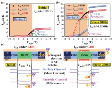
Fig. 4. Comparison of ICP curves under different operation conditions
at (a) initial state and (b) after HCS, assuming the ICP contributions from
the gate oxide/HVNW interface are the same at initial state and after HCS. (c) Schematic of top view and energy band diagrams for surface and parasitic channels at initial state and after HCS.
This causes both the main current and off-current to turn-off, as shown in Fig. 1(b).
From the comparison of charge pumping current (ICP)
between different operation conditions, such as the source/ drain/body all grounded (GSDB), GSDB with drain floating (GSB) and GSDB with source floating (GDB), the position of interface degradation can be clarified. The ICPunder GDB
in the off region increases significantly after HCS as shown in Fig. 4(b). This result indicated that the most interface degradation is in the gate to PDDD overlap region at drain side. Nevertheless, the degraded interfaces include the gate oxide/PDDD and STI/PDDD interfaces. On the other hand, the analysis of charge pumping (CP) measurements at different operation conditions are helpful to demonstrate the formation of the parasitic channel. Fig. 4(a) shows a comparison of ICP curves under different operation conditions at initial state.
In this figure, we can subtract the ICP contribution from the
gate oxide/HVNW interface (ICP,SC) as well as subtracting
the maximum ICPunder GSB in the off-state (ICPOFF,0s) from
the maximum ICP under GDB. The intersection point of a
horizontal line drawn from the subtraction result to the ICP
curve under GDB corresponds to one specific pulse high level (Vhigh). Clearly, the specific Vhigh is about threshold voltage
for the initial state, as can be seen in Fig. 4(a). In fact,
this specific Vhigh is the critical voltage for probing ICP from
the contribution of interface traps in the gate to PDDD overlap region at the source side (Nit,S) under GDB. Because the path
for off-current is not formed at initial state, in order for the ICP
under GDB to include Nit,S, the surface channel needs to be
turned-on as in the left side of Fig. 4(c). Therefore, the critical voltage is about the threshold voltage of the device. However, the critical voltage shifts to about 3.5 V after HCS, as shown in Fig. 4(b). This means that the critical voltage for probing ICP
under GDB with Nit,S is 3.5 V. As can be seen on the right
of Fig. 4(c), when Vhigh is at 3.5 V, the surface channel is
not turned-on. Therefore, ICP under GDB includes Nit,S
through the parasitic channel when Vhigh is at 3.5 V.
Consequently, this analysis of CP measurements confirms the formation of the parasitic channel after HCS.
IV. CONCLUSION
The abnormal off-current behavior induced by the HCS in p-channel DDDMOS transistors with STI structure has been investigated in this work. Because there are strong ED,SUR.,
ED,BULK at the drain-side corners under HCS, and a nitride
layer in STI, electrons generated by impact ionization at drain-side corners can be accelerated into the deep region of HVNW and then these hot electrons can be easily trapped in STI. Furthermore, electron trapping in STI progressively extends from drain to source during HCS. Then the conductive path for off-current at the STI edge is formed. This leak-age path is further demonstrated by the comparisons of CP measurements at different operations between initial state and after HCS.
REFERENCES
[1] K. Nomura et al., “Room-temperature fabrication of transparent flexible thin-film transistors using amorphous oxide semiconductors,” Nature, vol. 432, pp. 488–492, Nov. 2004.
[2] C. T. Tsai et al., “Influence of positive bias stress on N2O plasma
improved InGaZnO thin film transistor,” Appl. Phys. Lett., vol. 96, no. 24, pp. 242105-1–242105-3, 2010.
[3] T. C. Chen et al., “Behaviors of InGaZnO thin film transistor under illuminated positive gate bias stress,” Appl. Phys. Lett., vol. 97, no. 11, pp. 112104-1–112104-3, 2010.
[4] T. C. Chang et al., “Developments in nanocrystal memory,” Mater.
Today, vol. 14, no. 12, pp. 608–615, Dec. 2011.
[5] M. C. Chen et al., “Influence of electrode material on the resistive memory switching property of indium gallium zinc oxide thin films,”
Appl. Phys. Lett., vol. 96, no. 26, pp. 262110-1–262110-3, 2010.
[6] Y. E. Syu et al., “Redox reaction switching mechanism in RRAM device with Pt/CoSiOX/TiN structure,” IEEE Electron Device Lett., vol. 32,
no. 4, pp. 545–547, Apr. 2011.
[7] Y. H. Lee et al., “Channel width dependent hot carrier degradation of thin gate pMOSFETs,” in Proc. IEEE 38th Annu. Int. Rel. Phys. Symp., San Jose, CA, Apr. 2000, pp. 77–82.
[8] S. S. Chung et al., “New degradation mechanisms of width-dependent hot carrier effect in quarter-micron shallow-trench-isolated p-channel metal-oxide-semiconductor field-effect-transistors,” Jpn. J. Appl. Phys., vol. 40, no. 1, pp. 69–74, Jan. 2001.
[9] S. S. Chung et al., “Impact of STI on the reliability of narrow-width pMOSFETs with advanced ALD N/O gate stack,” IEEE Trans. Device
Mater. Rel., vol. 6, no. 1, pp. 95–101, Mar. 2006.
[10] M. Koyanagi et al., “Hot-electron-induced punchthrough (HEIP) effect in submicrometer PMOSFET’s,” IEEE Trans. Electron Devices, vol. 34, no. 4, pp. 839–844, Apr. 1987.
[11] L. Selmi et al., “Measurement of the hot hole injection probability from Si into SiO2 in p-MOSFETS,” in Proc. IEEE IEDM, Dec. 1993,