New design techniques for a complementary
metal-oxide semiconductor current readout
integrated circuit for infrared detector arrays
Chung-Yu WuChih-Cheng Hsieh
National Chiao lung University
Department of Electronics Engineering and Institute of Electronics
Integrated Circuits and Systems Laboratory 1001 Ta-Hsueh Road
Hsinchu, Taiwan 300
E-mail: p791 1 581 @alab.ee.nctu.edu.tw
1 Introduction
Thephotovoltaic (PV) infrared (IR) detector is potentially suitable for the applications in low-power, large-area second-generation multispectral IR imagers because it has a much larger sensor resistance than the photoconductive JR detector. In the readout operation ofthe PV JR detector, voltage readout and current readout are the two popular approaches. Usually, the current readout is chosen because of the noise, bias point,
and the power dissipation consideration.
Because the PV JR detector device is reverse biased, both surface generation-recombination current and surface tun-neling current are increased, which causes the 1 Ifnoise
to
increase proportionally."2 Moreover, the device bias also leads to the bias-induced dc currents. Clearly, maintaining a low detector bias is important for the current readout cir-cuit to minimize the noise and the excess dc current of JR detectors.
Generally, the total input referred noise current of an JR detection channel is made up of four components: back-ground optically generated shot noise, detector noise, input stage noise, and signal processing stage noise. The goal of a current readout structure is to make the other three noise components less than the background shot noise, so that only the inevitable background shot noise dominates. According to this requirement, the current readout input stage needs to
Abstract. A new share-buffered direct-injection (SBDI) current readout circuit with high injection efficiency, low noise, high dynamic range, and good threshold control is proposed. The circuit is superior to the tradi-tional direct-injection (Dl) current readout circuit. Using the SBDI readout circuit, the same excellent performance of the buffered direct-injection (BDI) current readout can be achieved, but only half the chip area and power consumption are required. Thus the SBDI is more suitable for infrared (IR) readout applications, especially for 2-D focal plane arrays under strict power and area limitations. A dynamic discharge source fol-lower (DDSF) output stage is also proposed and analyzed. It can im-prove the speed performance of the conventional source-follower output buffer and requires very little power dissipation. Both simulation and ex-perimental results have verified the functions and the advantageous fea-tures of the proposed readout structure.
have a very small input impedance to achieve a high injection efficiency. Otherwise, less signal and background shot noise from the detector are injected, and hence the noise of the readout structure becomes more significant to degrade the system noise performance [noise-equivalent difference in temperature (NELT) sensitivity].
So far, several current readout schemes and structures such as the source follower per detector5 (SFD), the capacitive transimpedance amp1ifier'5 (CTIA), the direct injection"6'7 (DJ),andthe buffered direct injection"3'68 (BDJ), have been proposed. Among them, both SED and DJ schemes have the problems of poor injection efficiency and nonuniform de-tector bias. Jn the CTJA, the reset operation induces a certain amount of clock feedthrough on the detector node and limits the output swing. Jn the BDJ, the additional chip size and power dissipation of the buffer often become intolerable, especially in large and high-performance focal plane arrays (FPAs).
Jn this paper, a new current readout scheme called the share-buffered direct injection (SBDJ) is proposed to solve the mentioned problems and improve the readout perfor-mance. Jt has been shown from both simulation and exper-imental results that the proposed SBDI has the same high injection efficiency and good zero-bias stability as the BDI. But the SBDJ has less chip area and power dissipation than the BDJ. Thus the SBDJ is suitable for the large and high performance 2-D JR detector array.
Jn Sec. 2, the circuit structure of the new SBDJ readout input stage is described and comparisons with DJ and BDI Subject terms: IR focal plane arrays; detectors; IR imaging; readouts; integrated circuits; injection efficiency.
Optical Engineering 34(1), 160—168 (January 1995).
Paper 17014 received Jan. 17, 1994; revised manuscript received Apr. 29, 1994; accepted for publication July 13, 1994.
1995 Society of Photo-Optical Instrumentation Engineers. 009 l-3286/95/$6.00.
160/OPTICALENGINEERING / January 1995 / Vol. 34 No. 1
in injection efficiency, noise performance, power require-ment, area consumption, threshold control, and 2-D appli-cation possibility are also discussed. In Sec. 3, a dynamic discharge source-follower output stage, including correlated double sampling (CDS) and autoclamping, is described. The speed performance, output range, and power dissipation of this output stage are also analyzed. In Sec. 4, both simulation results and experimental results of the fabricated SBDI read-out chip are presented. Finally, a conclusion is given.
2
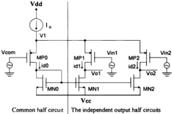
SBDI Current ReadoutInthe proposed new SBDI structure, a differential-input-to-single-ended-output amplifier with one commonly shared half circuit and several independent output half circuits are used. Figure 1 shows the circuit structure of the differential amplifier with common half circuit in the left and two in-dependent half circuits with V01 and V02 outputs in the right. This amplifier is used to describe the operating principle.
In the circuit of Fig. 1, Jo is the ideal bias current source; V1 and V12 are the two input signals; Vcom is the reference input voltage in the common half circuit; V01 and v02 are the two output voltages; and edO' 'dl' and 'd2 are incremental drain currents of MPO, MP1, and MP2, respectively. Because is a constant current source, we have
ldO+ldl+ld2O
Because all MPO, MP1, and MP2 are in saturation, the in-cremental drain currents can be written as
V1)
i1g01(V11—V1) 1d2gmj(Vjn21)
where isthe input transconductance of the amplifier. From
Eqs. (1) and (2), we have
V10 + V11
+
V12 V1=
3[
(V10+V1+V2
ldOmi[VinO
3 (2V10 —'in1—V7 (2v0, V() —'in2'dl—gmi
(2V2—VO—V, 'd2—g011 3Because transistors MNO, MN 1, and MN2 form a current mirror and hence the currents through MN1 and MN2 satisfy the relation tc/MNI =1dMN2=1dMNO = 'dO Thus the total
cur-rents sent to the output nodes V01 and V02 are — =
2d1+ 1d2 and 'd2 —td()=2(/2+d1' respectively. Because the output node V01 (V02) is loaded by the drain resistance of the input gates MP1 (MP2) and the load gates MN1 (MN2),
—— Vil—Vio
g
gd,+ j/
Vdd Vin2 Vcc MN2Common half circuit The independent output half circuits
Fig. 1 Differential-input-to-single-ended-output amplifier with one shared half circuit and two individual output half circuits.
respectively, the output node voltages V01 and v02 can be expressed as
2dl+d2
V01 =gmi ' (5a) gdi+
gdl 2d2+dl V02 gmi'
(5b) gdl+
gdlwhereg(g) is the output conductance of the input (load)
(1) transistors MP1 and MP2 (MN1 and MN2). From Eqs. (4a) and (4b), Eqs. (5a) and (5b) can be rewritten as
(
4V1 2V0 —2V2 2V2 V0 (2a) V01—gmi
+
3 (2b) (6a) (2c)I
4V22V02V1
2v11 —V0—v12V0=—g,,
3+
3 (3) V2=—g
. (6b) gdl + dlThenthe differential gains Adml and Adm2 are
V01 g01 V02
(4a) Adml
=
—
=
Adm2 (7)
V,j
,
g1+
'2 10It can be seen from Eqs. (6a) and (6b) that the output v01 of (4b) the first half circuit is independent of the input v12 of the
second half circuit, and similarly 2 is independent of Throughthe analysis, it is proved that the common half circuit 1'4 \ of the differential amplifier can be shared by several output k c1 half circuits and the gain characteristics can be kept the same as those of a single differential amplifier, without cross-interference among several input voltages.
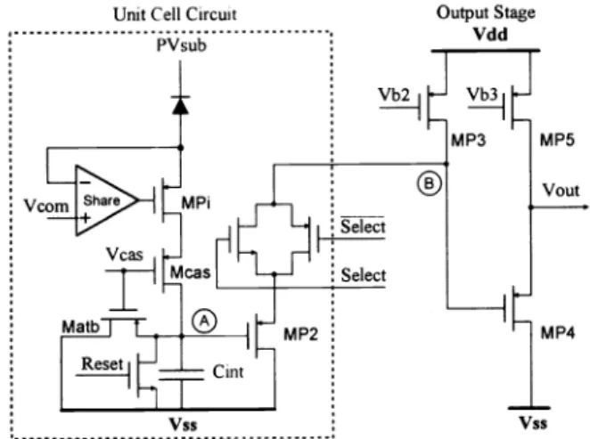
The input stage of the SBDI current readout scheme is shown in Fig. 2 where the original BDI circuit is separated into two parts: one is the common half circuit of the differ-ential amplifier shared by all the detector cells and the other is the remaining circuit of the BDI, which must be included in each cell. To connect the shared halfcircuit with each cell,
PVsub
IR PV Sensor
VcomL1H
lid
Fig. 2 Functional block diagram and complementary metal-oxide semiconductor (CMOS) circuit of the SBDI input stage.
threeglobal lines Vbl, common S, and common G are used, as shown in Fig. 2. An extra current-source metal-oxide semi-conductor (MOS) device is also used in each cell to obtain a stable source-coupled current source I. This device can minimize the mismatch effect and the route loading effect on the cunent source I. Totally, there are three MOS devices instead of a complete buffer amplifier in each cell to achieve the SBDI function.
In the SBDI circuit ofFig. 2, a cascade structure consisting of Mcas and MPi is used to minimize the clock feedthrough and reset signal coupling. The Matb device is an antiblooming gate to avoid the saturation condition. When the input signal current is large and the integrated voltage on the capacitor Cint approaches to Vcas + VT, the MOS device Mcas would be driven into the linear region and the effect of the cascade structure would be greatly degraded. In this undesirable sat-uration case, Matb is turned on to bypass the input signal current and then the integrated voltage is held constant in-dependent of the input signal_current. The two complemen-tary clock phases Select and Select are applied to the trans-mission gate to sample the integrated voltage on C1 after the integration time interval After sampling, the Reset clock signal resets the capacitor immediately.
In the following, the injection efficiency, noise perfor-mance, chip area, bias stability, and threshold uniformity control of the proposed BDI structure are described in detail. 2.1 Input Impedance and Injection Efficiency Themain design goal of the current readout input stage of IR detectors is to achieve a high injection efficiency and low noise. The injection efficiency i(s) and the bandwidth fBw of a Di structure can be expressed as168
g07R /
2\
i
+gR
l
+s/2fBW)
—1+ grn RD
fBw
2ITRDCT
The injection efficiency and the bandwidth of a BDI are
162/ OPTICAL ENGINEERING / January 1995/ Vol. 34 No. 1
(1+A)gR (
1\
ii(s)=
II '
(9a)1+(1+A)g01R \l+5/2lTfBw/
1 +(1 +A)gR
fBw= . (9b) 2irRDCTIn the preceding equations, A is the gain of the buffer, g is the transconductance of the input gate, and RD(CT) is the total input shunt resistance (shunt capacitance) of the JR de-tector. From Eqs. (8a), (8b), (9a), and (9b) it can be clearly seen that the injection efficiency i(s) and the bandwidthfBw are much improved in the BDI structure because the input impedance of the input gate MPi is reduced from 1 /g to 1 1(1 + A )g by using an actively compensated input struc-ture. This good injection efficiency and wide input bandwidth performance are also kept the same in the SBDI of Fig. 2 with the gain Adm in Eq. (7) substituted into the gain A in Eqs. (9a) and (9b). Typically, the gain amplitude Adm of the share-half circuit differential amplifier can be designed as 100,thenthe injection efficiency will be closed to 1 and the bandwidth will be almost 100-fold wider than that of the DI scheme if RD 5 large enough such that g0R > 1. 2.2 Noise Performance
Thenoise of the readout input stage should be significantly smaller than the noise produced by the JR detector and the radiation shot noise. The noise model of DI and BDI input stages can be represented by the models shown in Figs. 3 and 4, respectively. In the DI input stage, the noise generated by the input gate MOS is represented symbolically by an equivalent voltage source e connected to its gate, as shown in Fig. 3. An JR PV sensor can be modeled as a current source Ic with the shunt capacitor CD and the shunt resistance RD. (8a) Then the input referred noise current of the input stage can
be expressed as9 (8b)
i=g1e ,
(10)/
1/ 22 — 2 21
Omje
tn,DI —gje,7 — 2 \RD+1/gj/ (RD+ 1/gj)
Thus 'n,BDI inversely proportional to the gate transcon-ductance g . ComparingEqs. (1 1) and (14), the noise re-duction ratio is e(input MOS)/e1 (OP input gate), that is, the transconductance ratio gmjop'gmjcG of the OP input gate and the common-gate (CG) input as applying Eq. (15) to it. The transcondutance of the MOSFET is proportional to its operating current d Thus, it is apparent that a noise reduction ratio equal to the ratio of OP bias cunent over detector current can be obtained. Because the background photo-current is very small, a quite small bias photo-current of OP is enough to obtain a good noise performance.
The input referred noise current of the SBDI input stage is generally similar to that ofthe BDI in Eq. (14).It is apparent (11 ) fromEq. (14)that the input gate-referred noise e1 of the OP
gain stage dominated the noise performance. Thus only the input gate-referred noise of the shared half-circuit differ-ential pair in the SBDI scheme is analyzed. The correspond-ing noise model is shown in Fig. 5. To consider the noise contribution in each half circuit without confusion, the noise models of some MOS devices are expressed by the equivalent noise current source i in parallel with the drain-to-source channel, instead of the gate-referred noise voltage e. The value of equivalent noise current source i is with
given by Eq. (15).
From Fig. 5 and Eq. (6a), it is seen that the output noise voltage v01 is independent of the noise sources e3 and i6 of (12) the other half circuit. Thus the noise contribution of the other half circuit stage is zero. In this case, the noise contribution of each MOS device to the output noise voltage v01 in Fig. 5 can be expressed as
v01(efll)=Adfl7lefll , (16a)
v01(efl2)=Ad0Ie,72 , (16b)
Fig. 4 Noise model and equivalent circuit of the BDI input stage.
eli PVsub JR v Sensor Vcas id JR PV Sensor Equivalent Circuit eh Vcas PVsub
id
Fig. 3 Noise model and equivalent circuit of the DI input stage.
DI
'if
R>>l/gj
where 1d the drain noise current flows in the input gate generated by e,1 and i, is the input referred noise current. For low RD detectors, the stages have a high input referred noise current, as shown in Eq. (11).
On the other hand, the input referred noise of the BDI input stage, as shown in Fig. 4, is given by the superposition of the OP input gate referred noise voltages e1 and the noise voltages of the input MOS devices e2. The input referred noise current generated by e1 is
2
2 _enl
'n1j2
DThe input referred noise current generated by e2 is
2
2 2 F
1/(1+A)g01 12 e2/(1+A)22
en2
(13)
(1+A)2R
Because RD>> 11(1 + A the total input referred noise current of the BDI input stage is given by summing Eqs. (12) and (13) as
2 2 2
1iBDI =fl1
+ =
+
(1 +A)2R, (14)
The gate referred noise voltage source of a MOS field effect transistor (MOSFET) can be represented ast°
n 3g
PVsub
JR v Sensor
vcc
C2
(15) Fig. 5 Noise model and equivalent circuit of the differential pair withone shared half circuit and two individual output half circuits.
JRPV Sensor 2 EquivalentCircuit
VcomL>&4
I . PVsubVcas j
Id Vcas Id• l,i4 'n4
v01(i4)=
=
g+g5
•
l5
t,5v01(i5)=
=
g+g5
whereAdmj is the differential gain calculated in Eq. (7) with
=
d2 and=
Because these sources are all uncor-related, the overall mean-square output voltage v1 can be expressed asv1 =v1(e1) + v1 (e2) + v1 (i4) + v1 (i5)
(i4+i5)2
Ami(ei +e,2)+
(d2
+g5)Hence, the equivalent input noise voltage e1 =v01/Adm has
the mean-square value i14 + i5
=
e1+ e2 +g,2
= e1
+ e2+(g5/g72)2(e4 + e5)
where g4 g,,5 Hence, to minimize and the
contribu-tion of i4 and i, ,
clearly 2 should be much larger than5 'andthis is the normal design guide for the differential
input stage. Through the analysis, it is shown that the SBDI input stage can achieve a better noise performance over the DI, just as for the BDI structure.
2.3 Power Consumption and Chip Area
The total power consumption and unit-cell area for large FPAs are limited by practical considerations of cryogenic capability and package integrity of the JR detector systems. The conventional DI structure uses a single MOS device as the input stage and results in a low injection efficiency and low performance, although it has less power consumption and smaller chip area as compared with other readout schemes. Jn the BDI structure, better performance can be achieved, but the input stage of each cell requires an addi-tional buffer. Normally, the buffer is designed as a differential pair, which requires at least five MOSFETs and an additional power dissipation 2Id(Vdd— with 'd being the bias cur-rent in each half circuit. Jn the new SBDI structure, the input stage of each cell requires only three MOSFETs and its power dissipation is jdWdd Both power dissipation and chip area of the input stage buffer of the SBDI are only half of those in the input stage of BDI. As compared with the corn-monly used DI readout structure, there are only three extra MOSFETs of the buffer required in each cell. This increasing chip area is still tolerable in a high-density 2-D FPA with O.8-pm CMOS process. Thus this new SBDI readout struc-ture offers an effective trade-off between the readout per-formance and the chip area consumption.
The total devices count of the SBDJ unit cell is 10 MOS, as shown in Fig. 2. But it can be reduced to seven MOS devices by eliminating the cascade gate Mcas, the antibloom-ing gate Matb, and replacantibloom-ing the transmission gate by a santibloom-ingle p—channel MOS (PMOS) device. Without these performance options, the basic readout circuit operation remains un-164/OPTICALENGINEERING / January 1995/ Vol. 34 No. 1
(16c) changed. With the same basic operation, the DI structurerequires four MOS devices in total, whereas the BDI structure nine MOS devices. In applying the SBDJ to the 2-D FPA, 116d
)
the chip area can be further reduced by using a high-densitycapacitor process or the shared capacitor design technique. Jn a hybrid focal plane, the detector elements and the readout signal processor are fabricated on separate semicon-ductor substrates and then joined together using the array-bonding technique. The cell chip area of the current readout CMOS circuit in such a hybrid focal plane is limited to that of one single detector with a bonding pad. Thus, the complex buffer circuit used in the BDJ is not allowed in such a 2-D application with strict size limitation. Because the new SBDI
l7
input stage has low power dissipation and small chip area,J it can be used in the hybrid FPA.
Jn addition to high injection efficiency, good noise per-formance, small area size, and low power dissipation, good bias stability and threshold control are inherent in the SBDJ structure as well as in the BDI structure. The detectors should be kept near zero bias to prevent the generation of 1 /f noise and maintain linear and uniform response. The virtual short-circuit property between the two differential-pair OP input (18) nodes in the SBDI structure makes the detectors biased at
near zero bias.
Usually, strict threshold uniformity is required for an JR FPA sensor. Because the threshold voltage variation in the DJ input gate is directly coupled to the detector bias point, control of the FPA' s readout uniformity is difficult under the process variations. This problem can be solved by the SBDJ feedback amplifier structure. The threshold variation range of the feedback amplifier is equal to the random offset level of the OP amp. This is enough to satisfy the operational requirements dictated by JR detectors.
3
Dynamic Discharge Source-FollowerOutput Stage
Theoutput stage of a current readout circuit is also used as an unit-gain buffer and is usually implemented by source followers. As shown in Fig. 6, the signal voltage from each cell is sampled through the source follower by clocking the appropriate switches. The cascaded two stages of the source followers constructed by MP2 —MP5are used to drive the output load under high readout frequency. Because large charging and discharging currents through the output load are required to satisfy the requirements of frame rate and readout speed, the power dissipation of the output stage dom-mates that of the whole IR current readout circuit.
The function of this conventional source-follower output stage is described in the following. After the cell (n —1) readout operation is completed, node B is reset to a low level,
which is usually (V + Vgs(Mp2)) and V0 is reset to
(V+ Vgs(Mp2)+ Vgs(Mp4)). Then, before the sample-to-output operation of the cell (n), the voltage at node A is the integrated signal voltage, which is usually a high level be-cause of the integration of the input background current. Jn the sampling phase, Select is high and the transmission gate is on. At this time, MP2 is off because V(A)> V(B). But node B is gradually charged toward V(signal) + Vgs(Mp2) by the constant current through MP3. Jn the reset phase, Reset is high and V(A )is discharged to V immediately. Thus, there is a large drop between nodes A and B, which causes
MP2 and then MP4 to sink a large current and discharge the output node quickly. In this output stage, the speed is limited by the constant charging current generated by Vb3 and MP5, whereas the standby power dissipation is also determined by the constant charge current. A trade-offexists between power dissipation and readout frequency. The mentioned speed limit can be overcome by using a dynamic discharge source-follower output stage with only dynamic power dissipation. The dynamic discharge output stage, which is composed of a PMOS level shifter and an N-type MOS (NMOS) source follower with the dynamic discharge gate MN3 is illustrated in Fig. 7. The function of the dynamic output stage in the charging and reset phases is shown. In the charging phase, node B of the output stage is preset to a low level in the last cell reset phase. At this time, node A has a signal level of V(A ). Whenthe control signal Select is high, signal A is
sampled to the output stage and node B is charged to
V(A )+
Vgs(Mp2) quickly because it is only loaded by the switch transistors and the gate capacitance of MN! .Thehigh voltage at node B leads to a low V0rn in the sample moment. Then there is a large voltage drop between gate and source nodes of MN 1 ,whichgenerates a large charging current to charge the output load to V(B) —Vgs(MN1)quickly. In the reset phase, node A is discharged to through the reset switch and node B is discharged to V+ Vgs(Mp2)immedi-ately. At this time, V0 is pulled to a low voltage of
vss + Vgs(Mp2) Vgs(MN1) by the constant cunent of MN2 and the extra dynamic discharge gate MN3 controlled by the clock D,rst. Because is high when Reset is high, the output voltage is discharged to low through MN3 in every reset phase. This achieves a high readout speed without any extra static power dissipation. The dynamic discharge NMOS source follower can be applied to both n-on-p and p-on-n types of detectors that have the reset-to-low operation and the high signal output level in the output stage.
The maximum integrated voltage on C1 in each cell is constricted to Vim in the conventional PMOS cascaded source followers output stage in Fig. 6. To cause all the MOS tran-sistors to work in the saturation region, the maximum output voltage should obey
V VddHVdsat(Mp
out (19)where Vdsat(Mp5) is the saturation voltage of MP5. Thus, the
Viflt Vdd— Vdsat(Mp5)— Vgs(Mp4)— Vgs(Mp2)
because
Vout =
Vfl
+ Vgs(Mp2) + Vgs(Mp4)(20)
(21) Because the dc drain current of MP4 is equal to that of MP5, which must be large enough to charge/discharge the output load, the voltage Vgs(Mp4) 5 large. As can be seen from Eq. (20), the maximum signal integrated voltage is seriously de-graded and results in a low dynamic range. The case is even worse under cryogenic operation with a larger threshold volt-age than that under room-temperature operation.
In the dynamic discharge output stage, as shown in Fig. 7, a large integration capacity can be achieved by using a complementary type of cascaded source followers. The max-imum output voltage Vout and the integrated signal voltage V10 are
Vout V0+ Vgs(Mp2) —Vgs(MN1)Vdd— Vdsat(MN1) , (22)
Vdd— Vdsat(MN1) Vgs(Mp2) + Vgs(MN1) (23)
Equation (23) shows that the maximum input signal inte-grated range is increased without the degradation by the out-put stage. This structure can also achieve an almost zero dc offset by properly tuning the voltages Vgs(Mp2) and Vgs(MN1). Note that the smallest voltage Vout must obey the condition
V Vdsat(MN2)out (24)
where Vdsat(MN2)5 the saturation voltage ofMN2. To achieve the minimum V00 'onecan choose
Vgs(Mp2) =Vgs(MN1)+ Vdsat(MN2) (25)
In this case, V00 5 minimum without losing the
low-background signal. Through the analysis, it is seen that the dynamic discharge output stage with complementary cas-caded source followers can improve the dynamic range and overcome the speed limit of the conventional output stage at the small cost of increasing the dynamic power dissipation.
Unit Cell Circuit Output Stage
Vdd Dynamic DischargeVdd Ouput Stage
Fig. 6 Conventional PMOS cascaded source-follower output stage.
Fig. 7 Dynamic discharge output stage with the level shifter.
The additional clock control can be shared with the CDS stage, as shown in Fig. 8, which can eliminate the 1 /f noise of multiplexer and output stage.8"'3
4
Simulation and Experimental ResultsFigure9 is a block diagram of a N X 1 scanning array readout circuit using SBDI technology. It is composed of an analog signal processing unit and a digital clock control unit. The pv sensors are connected to the readout chip through bonding pads. The bias circuit can be implemented on chip or off chip. The difference between common voltage Vcom and photo-detector substrate bias PVSUb deference determines the bias condition of detector. These can be connected together to achieve a zero bias. There is an optimum voltage Vcom to achieve the largest integrated capacity while keeping the am-plifier operating properly. Those voltages marked with * are optional, depending on different applications.
Because this readout chip is of mixed-mode circuits, some design techniques are used to offer good shielding between digital part and analog part. First, the whole n-substrate is biased by the analog power supply AVdd to avoid the noise coupling effect from the digital power supply to the substrate. In addition to this, analog and digital power supplies should be separated to avoid the digital noise resulting from the dynamic switching current of logic gates from being coupled to the analog part.
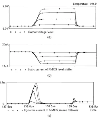
SPICE simulation results of the SGDI current readout with input signals 5, 50, and 100 nA and the maximum input background capacity 130 nA, are shown in Fig. 10. The
Dynamic Discharge Ouput Stage Correlated Double Sampling Stage
output voltage waveforms at the node Vout of Fig. 7 is shown in Fig. 10(a). The static current in the PMOS level shifter is shown in Fig. 10(b), where less 20 A is needed and the static power dissipation is small. The dynamic charging and discharging waveforms of the NMOS source follower are shown in Fig. 10(c). It is clearly seen that this output stage consumes only dynamic power and the total average power dissipation is small. As shown in the simulation results,
1 -MHz readout frequency can be achieved with a power dis-sipation below 10 mW at a 25-pF output loading and 10-V supply. Evidently, the summation ofthe output charging time and reset time in Fig. 10(a) is less than 500 ns, that is, the readout speed performance could be as high as 2MHz.
Several experimental circuits were designed and fabri-cated to verify this new CMOS readout circuit. Photographs of 8 X 1 and 64 X 1 SBDI experimental readout chips that were fabricated in 3-pm double-poly single-metal p-well CMOS process are shown in Figs. 1 1(a) and 1 1(b), respec-tively. An off-chip test current source is used to simulate the photocurrent of the JR detector and the experimental results are shown in Fig. 12 with different input currents in the first four cells and the same input current in the last four cells. The measured readout speed is 500 kHz, which is smaller than the simulated speed of 2 MHz. The charging speed decrease is caused by the inevitable extra load capacitance of the test environment, which is much larger than the normal load capacitance of the designed readout chip.
The measured current voltage (I-V) relationship results with the input current range from 50 to 120 nA by a 5-nA step are shown in Fig. 13. It is seen that the linearity per-formance of this chip can be larger than 98%. The voltage
I *
- %
138.Ous 138.5us 139.Ous 139.5us
Dynamiccurrent of NMOS source follower Time
(c)
Fig. 10 SPICE transition simulation results of the SBDI readout cir-cuit with input signal currents 5, 50, 100, and 130 nA (saturation):
J (a) waveforms of the output voltage (b) current flows in the NMOS source follower, and (c) current flows in the PMOS level shifter.
166/ OPTICAL ENGINEERING / January 1995/ Vol. 34 No. 1
Select
JL
Reset
JL
Dyrst ELFLJLLJ1
Temperature: -196.0
o o Outputvoltage Vout
(a)
Fig. 8 CDS output stage with the control clock Dyrst.
InSb Photovaltaic Infrared Sensor Array (NxI)
1 3m
(b)
First HaS Circuit unit Cell 1 j Unit Cell 2 ,, Unit Cell N,, Output Stage
: Vbl
CornmS CornmS iIiiiii CornmS Vb2m CmG :I
IVed:
01
1 37.5us
Mclk
Shift Register & Digital Control Clock Generator
Fig. 9 Complete block diagram of a N x 1 SBDI readout circuit.
Fig. 1 1 Chip photographs of (a) 8 x 1 and (b) 64 x 1 SBDI IR read-out chips.
between V0 and VOUt(CDS)isthe sum of the voltage on Ca-pacitor C(dSandthe gate-to-source voltage drop Vgs of the unit gain buffer in Fig. 8, which is implemented by MN5 and MN6, an on-chip NMOS source follower. The uniformity of an 8 X1readout test chip with off-chip current input is shown
in Fig. 14. The uniformity performance, although limited by the off-chip current source data resolution, is expected to be better than 99%. The total test performance of the SBDI readout chip is summarized in Table 1. The readout speed is dependent on the integration interval and the frame rate. A higher readout frequency is not necessarily for the 1 -D scan-ning array but is useful for the 2-D application. Three (0-, 5-, and 10-V) or two (0- and 10-V) power supplies are op-tional, depending on the power dissipation and chip area considerations. An additional power supply (5 V) used by the shared half-circuit differential pair can decrease the power dissipation and the chip size of the buffer in every cell. The power dissipation in Table 1 is calculated without considering the static power dissipation of the bias circuits.
1 8'/ — — t...' ...
.
..:..i. 1'II
illi I
1\-'d Lv 16.84s
Fig. 12 Measured output waveforms of the 8 x 1 SBDI readout chip with off-chip input current sources supplying the first four cells with four different input currents and the last four cells with constant input currents.
Fig. 13 Output voltage V0 and CDS output voltage VOUt(CDS) versus different input currents from 50 to 120 nA in 5-nA steps.
5 Summary
In this paper, a new SBDI current readout input stage and a dynamic discharge complementary cascaded source-follower output stage for IR detectors are proposed and analyzed. This new CMOS current readout structure uses a share half-circuit differential pair technique to implement a buffer with only half power dissipation and chip size as compared with the conventional BDI structure. It has been shown that the new current readout circuit has high injection efficiency, low noise, small chip size, low power dissipation, good threshold uniformity, high readout speed, and stable cryogenic tem-perature operations. Moreover, this new readout technology can be applied to FPA design and a high-performance 2-D (a)
—3.16s 2..LLs'dtu
(b)
ln.50n.—.— ln.60n.—A— In.70n. ln.80n.—.--- ln.90n.—+— ln.lOOn. +—+---—---+-———+--—----_+_____+-.--———+-——-—+ 3000. 2500. 2000-1500 1000 •—•- •—-—--—-—-—---—--—---——_ V—y----—-V--——V---V-—-——V——--y————v A—A----——_a---—----A—-—--A--——---A---—--_A_____A .—.—--——--.--—-——.—.---.——-—.—-——. .—.—_--—_-——-———.—-——-————_—-.--_—-—.—u
Fig. 14 Uniformity of the 8 x 1 SBDI readout chip with different input currents from 50 to 100 nA.
Table 1 Test results and operation conditions for the SBDI current readout structure.
Parameter Results
Power supply 0-5-by or 0-1OV
Max Photo-current
Max. Readout speed
Integration capacitance Storage capacity Transimpedance 130 nA 500k Hz > 2 pF > 1.0 x 10⁸e >40 MQ Power dissipation < 10 mW Linearity
Anti blooming control
Operation temperature >98%
yes
77 k
readout is achievable. The function and performance of this new SBDI readout structure are partly verified by experi-mental chips.
Acknowledgments
Wewould like to acknowledge the support and help of Sheng-Jen Yang, Tai-Ping Sun and Far-Wen Jih. This research was supported under the contract with the Chung Shang Institute of Science and Technology.
References
I. N.Bluzer and A. S. Jensen, '' 'Currentreadout of infrared detectors,"
Opt. Eng. 26(3), 241—248 (1987).
2. E. L. Dereniak and D. G. Crowe, "Noise sources,' 'Chap.3 in Optical
Radiation Detectors, pp. 75—78, Wiley-Interscience, New York (1984).
3. E. R. Fossum and B. Pain, ''Infraredreadout electronics for space sci-ence sensors: state of the art and future directions,' 'inInfrared
Tech-nology XIX, Proc. SPIE 2020, 262—285 (1993).
4. 0. Orias, A. W. Hoffman, and M. F. Casselman, "58 X 62 InSb focal plane array for infrared astronomy,' 'inInstrumentation in Astronomy VI, Proc. SPIE 627, 408-417 (1986).
5.A.' M. Fowler, R. G. Probst, J. P. Britt, R. R. Joyce, ad F. C. Gillett,
'Evaluationof an indium antimonide hybrid focal plane array for ground-based infrared astronomy," Opt. Eng. 26(3), 232—240 (1987).
6. K. Chow, J. P. Rode, D. H. Seib, and J. D. Blackwell, ''Hybridinfrared focal-plane arrays," IEEE Trans. Electron Devices ED-29(b), 3—13 (1982).
7. J. T. Longo, D. T. Cheung, A. M. Andrews, C. C. Wang, and J. M. Tracy, ''Infraredfocal planes in intrinsic semiconductors,' ' IEEE Trans.
Electron Devices ED-25(2),213—232 (1978).
8. A. H. Lockwood and W. J. Parrish, ''Predictedperformance of idium antimonide focal plane arrays," Opt. Eng. 26(3), 228—231(1987).
9. W. J. Parrish, ''Introductionto infrared focal plane electronics,' 'SPIE
SC-37, Orlando, FL (Apr. 1992).
10. R. Gregorian and G. C. Temes, ''Noisein MOSFETs," Chap. 3 in
Analog MOS Integrated Circuits for Signal Processing, pp. 96—99, Wiley-Interscience, New York (1986).
1 1 . R.J. Kansy, ''Response of a correlated double sampling circuit to
I /fnoise," IEEE J. Solid-State Circuits SC-15, 373—375 (1980).
12. H. M. Wey and W. Guggenbuhl, "An improved correlated double
sam-pling circuit for low noise charge-couple devices," IEEE J. Solid-State Circuits SC-37(12), 1 559—1 565 ( I 990).
13. L. Ramierz, R. Hickok, B. Pain, and C. Staller, "Implementation of a noise reduction circuit for spaceflight JR spectrometers,' ' inInfrared Readout Electronics, Proc. SPIE 1684,247—256(1992).
Chung-YuWu received the PhD degree from the Institute of Electronics, National Chiao Tung University, Hsinchu, Taiwan, in 1 980. From 1 980 to 1 984 he was an associate professor in the Department of Electronics Engineering and the lnstitute of Electronics, National Chiao Tung Univer-sity. During 1984 to 1986 he was an as-sociate professor in the Department of Electrical Engineering, Portland State Uni-versity, Oregon. He is a professor in the Department of Electronics Engineering and the Institute of Electron-ics, National Chaio Tung University. His research interests have been in analog/digital mixed-mode integrated circuit design, neural integrated circuit design, special semiconductor integrated devices and their applications, and device transient behavior analysis.
Chih-Cheng Hsieh received the BS de-gree in electronics engieering from Na-tional Chiao Tung University in 1990.
Since 1991 he has been working toward the PhD degree in the area of analog in-tegrated circuits and systems at the Insti-tute of Electronics, National Chiao Tung
University, Taiwan.
168/OPTICAL ENGINEERING / January 1995/Vol. 34 No. 1
Cell number