(SPDT) switches utilizing platinum (Pt, 70 nm) as the diffusion barrier have been studied and demonstrated. As compared with the Au-metallized switches, the Cu-metallized SPDT switches exhibited comparable performance with insertion loss less than 0.5 dB, return loss larger than 20 dB, isolation larger than 35 dB, and the input power for 1-dB compression (input P1 dB) of 28.3 dBm at 2.5 GHz. In order to evaluate the temperature-dependent impact on dc and RF characteristics of the copper-metallized switches for high-temperature applications, the switches have been tested at different temperatures. The device exhibits low thermal threshold coefficients (δVth/δT ) of −0.25 mV/K from 300 K to 500 K, good microwave performance
at 380 K with insertion loss less than 0.5 dB, isolation higher than 40 dB, and the input power for 1-dB compression (input
P1 dB) of 28.45 dBm at 2.5 GHz. To test the thermal stability of the Pt diffusion barrier, these switches were annealed at 250 ◦C for 20 h. After the annealing, the switches showed no degradation of the dc characteristics. In addition, after a high temperature storage life environment test at 150 ◦C, these copper-metallized switches remained capable of excellent power handling. To test the operation reliability of the copper-metallized switches, the copper-metallized switches were subjected to
ON/OFF(control voltage = +3/0 V exchange) stress test for 24 h at room temperature. The devices maintained excellent RF characteristics after the stress test. Consequently, it is successfully demonstrated through these tests that copper metallization using Pt as the diffusion barrier could be applied to the GaAs monolithic microwave integrated circuit switch fabrication with good RF performance, high-temperature characteristics, and reliability.
Index Terms—Copper metallization, platinum, pseudomophic
high-electron mobility transistor (PHEMT), single-pole–double-throw (SPDT), switch, temperature.
I. INTRODUCTION
C
OPPER has been used instead of aluminum as the in-terconnect metal for silicon integrated circuit technology since IBM adapted copper metallization in the silicon 0.18-μm technology [1]–[3]. The advantages of using copper metal-lization for Si technology include low resistivity and high electromigration resistance; however, there are only a fewManuscript received January 15, 2008; revised March 19, 2008. Current version published October 16, 2008. This work was supported in part by the National Science Council and in part by the Ministry of Economic Affairs, Taiwan, under Contracts NSC 94-2752-E-009-001-PAE and 94-EC-17-A-05-S1-020.
The authors are with the Department of Materials Science and Engineer-ing, National Chiao Tung University, Hsinchu 30010, Taiwan (e-mail: edc@ mail.nctu.edu.tw).
Digital Object Identifier 10.1109/TDMR.2008.2002493
interconnect metal has been extensively used for the manu-facture of GaAs-based field-effect transistors and monolithic microwave integrated circuits (MMICs), and the reliability of the metal system has been well proven. The application of copper as the metallization metal for GaAs devices has several superior advantages over gold, such as lower resistivity, higher thermal conductivity, and lower cost, as compared with gold. In this paper, we characterized the electrical performance of the copper-metallized AlGaAs/InGaAs pseudomophic high-electron mobility transistor (PHEMT) single-pole–double-throw (SPDT) switches and compare the performance with the gold-metallized GaAs SPDT switches.
Copper diffuses very fast into GaAs if without any diffusion barrier and forms a deep acceptor in GaAs, which leads to the failure of the electrical properties of the GaAs devices. It was demonstrated that TaN can be used as the diffusion barrier for the backside copper metallization on GaAs semiconductor field-effect transistors [4], [5] and that WNx can be used as
the diffusion barrier for copper airbridges on low-noise GaAs HEMTs [6]. Furthermore, Pt was used as the diffusion barrier layer for copper-metallized switches in recent years [7], and a gold-free fully copper-metallized InP heterojunction bipolar transistor was also realized using Ti/Pt/Cu nonalloyed ohmic contacts with Pt as the diffusion barrier in recent years [8]. It has also been demonstrated that the Ti/Pt/Cu system structure was very stable even after being annealed up to 350◦C and that copper started to diffuse through the Pt diffusion barrier and formed a Cu4Ti phase after being annealed at 400◦C, as inves-tigated by X-ray diffraction data, Auger electron spectroscopy depth profiles, and the sheet resistance measurement [9]. In this paper, the temperature-dependent characteristics of the copper-metallized switches are studied. The thermal stability of the Pt diffusion barrier and the electrical reliability are also investigated.
II. DEVICESTRUCTURE ANDFABRICATION
The AlGaAs/InGaAs PHEMT SPDT switch wafer was grown on a 4-in semiinsulating GaAs substrate by metal– organic chemical vapor deposition. The structure, from bottom to top, is composed of a 600-nm superlattice buffer, a 13-nm undoped InGaAs channel, a 3-nm undoped AlGaAs spacer, a delta-doped layer, a 37-nm undoped AlGaAs Schottky layer, and a 60-nm n+-GaAs capping layer, as shown in Fig. 1. The room temperature electron mobility and sheet carrier
622 IEEE TRANSACTIONS ON DEVICE AND MATERIALS RELIABILITY, VOL. 8, NO. 3, SEPTEMBER 2008
Fig. 1. Epitaxy structure of the PHEMT used in the copper-metallized AlGaAs/InGaAs SPDT switches.
concentrations of the device were 6500 cm2/V· s and 3.0× 1012cm−2, respectively.
The series/shunt SPDT switch process includes device active region definition, resistor formation, ohmic contact, gate forma-tion, device passivaforma-tion, capacitor, and interconnect formation. Wet etching with H3PO4-H2O2-H2O solution was used for device isolation and epitaxial resistor formation. The ohmic contacts were formed by Au/Ge/Ni/Au evaporation followed by rapid thermal annealing at 410◦C for 30 s. The citric acid and hydrogen peroxide mixed solution was used for the gate recess process. Ti/Pt/Au metal was used as gate metal, and the gate was formed by the lift-off process. Plasma-enhanced chemical vapor deposition silicon nitride film was used for passivation and as the dielectric for capacitors. A 30-nm Ti layer and a 70-nm Pt layer were used as the adhesion layer and the diffusion barrier layer, respectively, for the top plate of the capacitor and the bottom layer of the interconnects [7], [9]. A 2-μm-thick copper metal was electroplated on the Ti/Pt layers with a Cu seeding layer for interconnects. Then, the electroplated copper was annealed at 200◦C for 2 h for eliminating the hydrogen embrittlement effect [10] and obtaining the film with the lowest resistivity and the smoothest surface [11], [12]. Finally, a 100-nm-thick silicon nitride was deposited for final passivation. The AlGaAs/InGaAs PHEMTs used in the switches had a 0.5-μm gate length with dual fingers, and the drain-to-source spacing was 9 μm. The ohmic contact resistance for the PHEMTs was 0.12 Ω· mm, and the MIM capacitors used in the switches with 200-nm silicon nitride had a capacitance of 0.25-fF/μm2. A 3 kΩ of gate resistor between the signal and control terminal was designed to provide isolation between the signal and control paths. The circuit schematic of the series/ shunt SPDT switch is shown in Fig. 2. The control current of the GaAs SPDT switch is typically < 0.5 mA/mm.
III. RESULTS ANDDISCUSSION
The HEMTs in the switch fabricated using copper metalliza-tion showed similar dc characteristics in comparison with those
Fig. 2. Circuit schematic of the series/shunt SPDT switch.
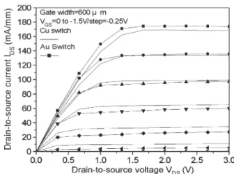
Fig. 3. I–V characteristics of AlGaAs/InGaAs PHEMT SPDT switches for 0.5-μm gate length with copper and gold metallizations.
Fig. 4. Extrinsic transconductance and drain-to-source current versus VGS bias characteristics of the AlGaAs/InGaAs PHEMT SPDT switches for 0.5-μm gate length with copper and gold metallizations.
in the switch fabricated with traditional gold metallization. As shown in Figs. 3 and 4, a drain saturation current density of 160 mA/mm and an extrinsic transconductance of 140 mS/mm at VDS= 3 V were measured both for the copper- and the Au-metallized switches. The devices had a threshold voltage (Vth) of−1.5 V. The insertion loss, return loss, and isolation characteristics of the SPDT switches with copper metallization and with gold metallization measured at 2.5 GHz are shown in
Fig. 5. Insertion loss and return loss versus frequency of the SPDT switches with copper and gold metallizations.
Fig. 6. Isolation versus frequency of the SPDT switches with copper and gold metallizations.
Figs. 5 and 6, respectively. The copper-metallized switch had an insertion loss of 0.33 dB, a return loss of 23.3 dB, and an isolation of 36.7 dB (control voltage = +3/0 V; input power = 0 dBm) at 2.5 GHz. There is very little difference in the RF characteristics for the switches with copper interconnects and with gold interconnects. The small differences of these two switches were due to the nonuniformity of the wet chemical etch in the gate recess process. The nonuniformity of the wet chemical etch could cause the fluctuation of the ON-state resistance and OFF-state capacitance of the transistors which dominate insertion loss and isolation [7]. It appears from these data that copper metallization does not affect the SPDT HEMT switch performance.
In order to evaluate the temperature-dependent effect on the dc and RF characteristics of the copper-metallized switches, the switches were evaluated at different temperatures. The dc characteristics of the device were measured at different temper-atures from 300 K to 500 K. Fig. 7 shows the current–voltage (I–V ) characteristics at different high-temperature ambients. The extrinsic transconductance and the drain-to-source cur-rent versus the temperature for the copper-metallized SPDT switches were shown in Fig. 8. A drain saturation current
Fig. 7. I–V characteristics of the 0.5-μm gate length PHEMT used in the copper-metallized switches tested at 300 K, 380 K, and 500 K, respectively.
Fig. 8. Extrinsic transconductance and drain-to-source current versus VGS bias characteristics of the 0.5-μm gate length PHEMT used in the SPDT switches when measured at 300 K, 380 K, and 500 K, respectively.
density of 188 mA/mm and an extrinsic transconductance of 159 mS/mm at VDS= 3 V at 300 K were measured for the devices. While the background carrier concentration from the substrate rises exponentially with temperature, causing the 2-DEG concentration (n2DEG) to increase in the active layer, the carrier velocity ν degraded seriously by the lattice scatter-ing and carrier–carrier scatterscatter-ing mechanisms [13]. Therefore,
IDSS0drops at high temperatures due to the enhanced scattering mechanisms even though the carrier concentration increases at high temperatures.
Furthermore, the gate leakage current (IG) as a function of
the gate-to-drain voltage (VGD) is shown in Fig. 9. When the gate-to-drain voltage was biased at −22 V, the gate leakage currents were 430, 450, and 490 μA/mm at the temperatures of 300 K, 380 K, and 500 K, respectively. The gate leakage current increases with increasing temperature mainly due to the tunneling mechanism with thermionic emission and partly caused by the reduction of barrier height [14].
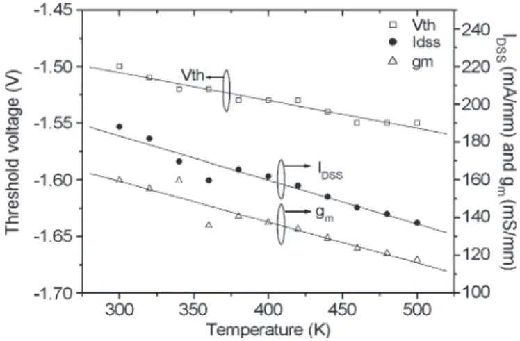
Fig. 10 shows that the Vthdecreases with increasing temper-ature. The Vthof a δ-doped HEMT can be obtained by solving
624 IEEE TRANSACTIONS ON DEVICE AND MATERIALS RELIABILITY, VOL. 8, NO. 3, SEPTEMBER 2008
Fig. 9. Gate leakage current (IG) as a function of the gate-to-drain voltage (VGD) for the PHEMTs used in the switches when tested at 300 K, 380 K, and 500 K.
Fig. 10. Threshold voltage (Vth), drain saturation current density (Idss), and extrinsic transconductance (gm) characteristics as a function of temperature for the copper-metallized AlGaAs/InGaAs PHEMT used in the SPDT switches.
the 1-D Poisson’s equation (1) as follows [13], [15]:
Vth= ΦB q − ΔEc q − n2DEG(dd+ Δd) ε . (1)
Among the aforementioned parameters, ΦB is the Schottky
gate barrier height, ΔEc is the conduction-band discontinuity
between the Schottky layer and the InGaAs channel, ddis the
distance between the gate and the n2DEGlocation, (dd+ Δd)
is the effective distance between the gate and the n2DEG location, and ε is the permittivity of the Schottky layer. Based on (1), while the temperature is increased, the threshold voltage decreases owing to the increase of the intrinsic channel carrier concentration n2DEG [13] and the lowering of the Schottky barrier height ΦB [16], [17]. Moreover, the decrease of Vth is partly caused by the leakage current from a semiinsulating substrate with increasing temperature [14]. Based on the rela-tionship of Vth= Vth0− K(T − T0), Vthis relatively temper-ature insensitive. The Vthshift from 300 K to 500 K was only
−0.05 V, and δVth/δT =−0.25 mV/K as a result.
As shown in Fig. 10, the maximum extrinsic transconduc-tance (gm,max) decreases with increasing temperature, which
Fig. 11. Insertion loss and isolation versus frequency of the copper-metallized SPDT switches measured from 300 K to 380 K.
Fig. 12. ON-state resistance as a function of temperature for the SPDT switches.
is attributed to the decrease of the intrinsic transconductance [13] and the increase of the ohmic contact resistance [18], respectively, as the previous reports. Therefore, it can be seen that when the temperature is increased, the degradations of the device performance include the increase of the leakage current and the decrease of the breakdown voltage, threshold voltage, extrinsic transconductance, and drain saturation current density. Furthermore, RF performances of the device were measured at high temperatures. Fig. 11 shows the insertion loss and isolation versus frequency of the SPDT switches with copper metallization from 300 K to 380 K. The isolation characteristics of the copper-metallized switches degraded slightly because of the increase of the leakage current from the semiinsulating substrate with increasing temperature. For this reason, the iso-lation is closely related to theOFF-state threshold characteristics which were affected by the leakage current. Although isolation of the copper-metallized switch was influenced by the ther-mal effect, it still maintained excellent isolation value higher than 35 dB.
In addition, the transistor had a small ON-state resistance which resulted in low insertion loss. However, the ON-state resistances of the copper-metallized switches measured at
VGS= 0 V and VDS= 0.5 V increased gradually from 300 K to 500 K, as shown in Fig. 12. The series resistance increased as
Fig. 13. Switching time as a function of temperature at 2.5 GHz for the SPDT switches.
the source, drain, and gate resistances increased with increasing temperature because of the carrier scattering [19] which would result in the reduction of the carrier transport velocity (υ) and the electron mobility (μe) in the channel due to the lattice
scat-tering and carrier–carrier scatscat-tering at elevated temperatures [13]. The degradation ofON-state resistance was also caused by the increase of the electrode contact resistance with temperature as verified in the previous reports [20]. This phenomenon led to the slight degradation of the insertion loss, but the increase in the insertion loss from 300 K to 380 K was only 0.08 dB, as shown in Fig. 11. Overall, for high-temperature operation, the copper-metallized switch had an insertion loss of 0.46 dB and an isolation of 42.79 dB (control voltage = +3/0 V; input power = 0 dBm) when tested at 2.5 GHz at 380 K. It is demonstrated that the copper metallization can be applied to the interconnects of the SPDT switches at high temperatures without affecting the switch performance.
Fig. 13 shows the thermal effect on the switching time for the copper-metallized switches. The switching time increases with increasing temperature primarily due to the degradation of the
ON-state resistance.
The power limitation of the switch operation is as ex-plained in [21]–[24], and the maximum input power Pmax is expressed as
Pmax=
(VC− Vth)2 2Z0
(2) where Z0 is the line impedance and Vc is the absolute of the
control voltage. It indicates that small threshold voltage and higher control voltage can improve the power handling capa-bility of the FET switch. The input power 1-dB compression and the second and third harmonic characteristics of the copper switches as a function of temperature measured at 2.5 GHz are shown in Fig. 14. The value of the input P1 dB with different temperatures remained considerably steady because the threshold voltage shift was small and did not influence the power handling capability. The characteristics of the second and third harmonics from 300 K to 380 K under the input power of 20 dBm are shown in Fig. 14. The second and third harmonics
Fig. 14. Input power 1-dB compression and second and third harmonic characteristics for the SPDT switches as a function of temperature when tested at 2.5 GHz.
Fig. 15. Input IIP3 as a function of temperature under different input power conditions at 2.5 GHz.
of the device remained quite stable during this temperature range. The harmonic performance is highly associated with power handling capability [25], and the input P1 dB was kept at about 28.4 dBm in the current case. Fig. 15 shows the input third-order intermodulation intercept point (IIP3) versus different temperatures under several input power conditions. The IIP3 value of the device was kept at different temperatures. IIP3 of 40.5 dBm was achieved at 380 K when the input power was 20 dBm. Based on the aforementioned results, it can be seen that the power handling capability was closely related to the threshold characteristics and that the temperature dependence of the power handling capability was not obviously from 300 K to 380 K.
IV. RELIABILITYTEST
The copper-metallized switches were annealed at 250◦C for 20 h in order to test the thermal reliability of the Pt diffusion barrier for long-term period. Although small degradation of the ohmic contact resistance was observed in Fig. 16, the drain saturation current density and the extrinsic transconductance were not obviously influenced after annealing at 250 ◦C for
626 IEEE TRANSACTIONS ON DEVICE AND MATERIALS RELIABILITY, VOL. 8, NO. 3, SEPTEMBER 2008
Fig. 16. I–V characteristics of the copper-metallized AlGaAs/InGaAs PHEMT SPDT switches for 0.5-μm gate length before and after annealing at 250◦C for 20 h.
Fig. 17. Extrinsic transconductance versus VGSbias characteristics of the copper-metallized AlGaAs/InGaAs PHEMT SPDT switches for 0.5-μm gate length before and after annealing at 250◦C for 20 h.
20 h, as shown in Fig. 17 (less than 1% difference in drain saturation current density and less than 3% difference in ex-trinsic transconductance). These results indicate that Cu–Pt interconnect layers are quite stable and that platinum is an effective diffusion barrier against copper diffusion after thermal annealing. Thus, the copper-metallized SPDT switches have maintained the electrical performance without any significant change during the high-temperature ambient test.
Fig. 18 shows the output power versus input power of the copper-metallized SPDT switches at 2.5 GHz after annealing at 150◦C under nitrogen atmosphere for different annealing time; the input P1 dB(input power for 1-dB compression) maintained the same level without any obvious degradation after the long-term test. Hence, the copper-metallized switches demonstrated very good reliability and showed similar switch power handling capability after 144 h of high temperature storage life (HTSL) environment test.
To test the operation reliability of the copper-metallized switches, the copper-metallized switches were subjected to an
ON/OFF stress test (control voltage = +3/0 V exchange) for
Fig. 18. Output power versus input power of the copper-metallized SPDT switches at 2.5 GHz after annealing at 150◦C for different annealing periods.
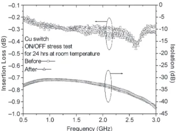
Fig. 19. Insertion loss and isolation versus frequency of the copper-metallized AlGaAs/InGaAs 0.5-μm PHEMT SPDT switches before and after ON/OFF
stress test for 24 h at room temperature.
24 h at room temperature. As shown in Fig. 19, the copper-metallized switches showed very little change after the stress test. The insertion loss and isolation still remained stable. Almost no obvious change in the insertion loss and isolation occurred, which indicated that no significant degradation of
ON-state resistance and OFF-state capacitance took place. It implies no copper diffusion into the active device region for the transistors after control voltage exchange stress for the copper-metallized SPDT switches using Pt as the diffusion barrier.
V. CONCLUSION
An SPDT GaAs switch fabricated with copper-metallized in-terconnects using Pt as the diffusion barrier has been fabricated and investigated. The copper-metallized SPDT switch exhibited an insertion loss of 0.33 dB, a return loss of 23.3 dB, and an isolation of 36.7 dB at 2.5 GHz; the performance is comparable with the performance of the traditional gold-metallized SPDT switches. The input power for 1-dB compression (input P1 dB) of 28.3 dBm at 2.5 GHz was obtained for these switches. Moreover, the temperature-dependent effects on the insertion loss, isolation, switching characteristics, and power handling
reliable process and can be applied to the GaAs MMIC switch fabrication.
ACKNOWLEDGMENT
The authors would like to thank Dr. S. H Tsai and H. C. Huang for the assistance in experiments.
REFERENCES
[1] K. Holloway and P. M. Fryer, “Tantalum as diffusion barrier between copper and silicon,” Appl. Phys. Lett., vol. 57, no. 17, pp. 1736–1738, Oct. 1990.
[2] K. Holloway, P. M. Fryer, C. Cabral, Jr., J. M. E. Harper, P. J. Bailey, and K. H. Kelleher, “Tantalum as a diffusion barrier between copper and silicon: Failure mechanism and effect of nitrogen additions,” J. Appl. Phys., vol. 71, no. 11, pp. 5433–5444, Jun. 1992.
[3] D. S. Yoon, H. K. Baik, and S. M. Lee, “Effect on thermal stability of a Cu/Ta/Si heterostructure of the incorporation of cerium oxide into the Ta barrier,” J. Appl. Phys., vol. 83, no. 12, pp. 8074–8076, Jun. 1998. [4] C. Y. Chen, E. Y. Chang, L. Chang, and S. H. Chen, “Backside copper
metallization of GaAs MESFETs using TaN as the diffusion barrier,” IEEE Trans. Electron Devices, vol. 48, no. 6, pp. 1033–1036, Jun. 2001. [5] C. Y. Chen, E. Y. Chang, L. Chang, and S. H. Chen, “Backside copper
metallisation of GaAs MESFETs,” Electron. Lett., vol. 36, no. 15, pp. 1317–1318, Jul. 2000.
[6] H. C. Chang, E. Y. Chang, Y. C. Lien, L. H. Chu, S. W. Chang, R. C. Huang, and H. M. Lee, “Use of WNx as diffusion barrier for copper airbridged low noise GaAs PHEMT,” Electron. Lett., vol. 39, no. 24, pp. 1763–1765, Nov. 2003.
[7] Y. C. Wu, E. Y. Chang, Y. C. Lin, H. T. Hsu, S. H. Chen, W. C. Wu, L. H. Chu, and C. Y. Chang, “SPDT GaAs switches with copper metal-lized interconnects,” IEEE Microw. Wireless Compon. Lett., vol. 17, no. 2, pp. 133–135, Feb. 2007.
[8] S.-W. Chang, E. Y. Chang, C.-S. Lee, K.-S. Chen, C.-W. Tseng, Y.-Y. Tu, and C.-T. Lee, “A gold-free fully copper-metallized InP heterojunction bipolar transistor using non-alloyed ohmic contact and platinum diffusion barrier,” Jpn. J. Appl. Phys., vol. 44, no. 28, pp. L899–L900, 2005. [9] S.-W. Chang, E. Y. Chang, D. Biswas, C.-S. Lee, K.-S. Chen,
C.-W. Tseng, T.-L. Hsieh, and W.-C. Wu, “Gold-free fully Cu-metallized InGaP/GaAs heterojunction bipolar transistor,” Jpn. J. Appl. Phys., vol. 44, no. 1A, pp. 8–11, 2005.
[10] G. Ananta Nagu, Amarnath, and T. K. G. Namboodhiri, “Effect of heat treatments on the hydrogen embrittlement susceptibility of API X-65 grade line-pipe steel,” Bull. Mater. Sci., vol. 26, no. 4, pp. 435–439, Jun. 2003.
[11] D. Kwon, H. Park, S. Ghosh, C. Lee, H. T. Jeon, and J. G. Lee, “Recrys-tallization of the copper films deposited by pulsed electroplating on ECR plasma-cleaned copper seed layers,” J. Korean Phys. Soc., vol. 44, no. 5, pp. 1108–1112, May 2004.
[12] P. Singer, “Copper CMP: A question of tradeoffs,” Semiconductor Inter-national, pp. 73–84, May 2000.
[13] C. S. Lee, Y. J. Chen, W. C. Hsu, K. H. Su, J. C. Huang, D. H. Huang, and C. L. Wu, “High-temperature threshold characteristics of a symmetrically graded InAlAs/InxGa1−xAs/GaAs metamorphic high electron mobility transistor,” Appl. Phys. Lett., vol. 88, no. 22, p. 223 506, May 2006. [14] W.-C. Liu, K.-H. Yu, K.-W. Lin, J.-H. Tsai, C.-Z. Wu, K.-P. Lin, and
C.-H. Yen, “On the InGaP/GaAs/InGaAs camel-like FET for high-breakdown, low-leakage, and high-temperature operations,” IEEE Trans. Electron Devices, vol. 48, no. 8, pp. 1522–1530, Aug. 2001.
transconductance stability,” IEEE Trans. Rel., vol. 39, no. 5, pp. 571–574, Dec. 1990.
[21] K. Miyatsuji and D. Ueda, “A GaAs high power RF single pole dual throw switch IC for digital mobile communication system,” IEEE J. Solid-State Circuits, vol. 30, no. 9, pp. 979–983, Sep. 1995.
[22] S. Makioka, Y. Anda, K. Miyatsuji, and D. Ueda, “Super self-aligned GaAs RF switch IC with 0.25 dB extremely low insertion loss for mobile communication systems,” IEEE Trans. Electron Devices, vol. 48, no. 8, pp. 1510–1514, Aug. 2001.
[23] H. Ishida, Y. Hirose, T. Murata, Y. Ikeda, T. Matsuno, K. Inoue, Y. Uemoto, T. Tanaka, T. Egawa, and D. Ueda, “A high-power RF switch IC using AlGaN/GaN HFETs with single-stage configuration,” IEEE Trans. Electron Devices, vol. 52, no. 8, pp. 1893–1899, Aug. 2005. [24] C.-K. Lin, W.-K. Wang, Y.-J. Chan, and H.-K. Chiou,
“BCB-bridged distributed wideband SPST switch using 0.25-μm In0.5Al0.5 As-In0.5Ga0.5As metamorphic HEMTs,” IEEE Trans. Electron Devices, vol. 52, no. 1, pp. 1–5, Jan. 2005.
[25] K.-H. Lee, Z. Jin, and K.-H. Koo, “High linearity SPDT switch for dual band wireless LAN applications,” in Proc. IEEE APMC, 2005.
[26] W.-C. Liu, K.-H. Yu, R.-C. Liu, K.-W. Lin, K.-P. Lin, C.-H. Yen, C.-C. Cheng, and K.-B. Thei, “Investigation of temperature-dependent characteristics of an n+-InGaAs/n-GaAs composite doped channel HFET,” IEEE Trans. Electron Devices, vol. 48, no. 12, pp. 2677–2683, Dec. 2001.
Yun-Chi Wu was born in Chiayi, Taiwan. He
re-ceived the B.S. degree in materials science and en-gineering from Tatung University, Taipei, Taiwan, in 2001 and the M.S. degree in materials science and engineering in 2003 from the National Chiao Tung University, Hsinchu, Taiwan, where he is currently working toward the Ph.D. degree in the Compound Semiconductor Device Laboratory, Department of Materials Science and Engineering.
His research is focused on HEMT device and process technologies for wireless communication applications.
Edward Yi Chang (S’85–M’85–SM’04) received
the B.S. degree in materials science and engineering from the National Tsing Hua University, Hsinchu, Taiwan, in 1977 and the Ph.D. degree in materi-als science and engineering from the University of Minnesota, Minneapolis, in 1985.
He was with the Unisys Corporation GaAs Component Group, Eagan, MN, from 1985 to 1988 and with the Comsat Labs Microelectronic Group from 1988 to 1992. He worked on the GaAs MMIC programs on both groups. He was with the National Chiao Tung University (NCTU), Hsinchu, in 1992. In 1994, he helped set up the first GaAs MMIC production line in Taiwan and became the President of Hexawave Inc., Hsinchu, in 1995. In 1999, he returned to NCTU with a teaching position, where he is currently the Head and Professor of the Department of Materials Science and Engineering. His research interests include new device and process technologies for compound semiconductor RFICs for wireless communication.
Dr. Chang is a Senior Member and a Distinguished Lecturer of the IEEE Electronic Device Society.
628 IEEE TRANSACTIONS ON DEVICE AND MATERIALS RELIABILITY, VOL. 8, NO. 3, SEPTEMBER 2008
Yueh-Chin Lin was born in Taipei, Taiwan. He
received the B.S. degree in nuclear engineering and engineering physics from the National Tsing Hua University, Hsinchu, Taiwan, in 1996, the M.S. de-gree in electrical engineering from Tsing Hua Uni-versity, Hsinchu, in 2000, and the Ph.D. degree in materials science and engineering from the National Chiao Tung University, Hsinchu, in 2006.
From 2004 to 2006, he was with the NTT Basic Research Laboratories. He investigated the growth of AlGaSb/InAs HEMT on an Si substrate by molecular beam epitaxy. He is currently a Postdoctoral Fellow with the Department of Materials Science and Engineering, National Chiao Tung University. His research interests include HEMT device growth and process technologies for wireless communication.
Li-Han Hsu received the B.S. and M.S. degrees
in materials science and engineering in 2003 and 2005, respectively, from the National Chiao Tung University, Hsinchu, Taiwan, where he is currently working toward the Ph.D. degree in the Compound Semiconductor Device Laboratory, Department of Materials Science and Engineering.
His research interests include high frequency packaging technology, microwave flip-chip packag-ing, hot-via interconnects for MMIC and RF-MEMS, and packaging integration of 60-GHz MCM trans-ceiver modules.