ELSEVIER Journal of Non-Crystalline Solids 187 (1995) 81-85
I O U R N A L O F
D fSfll
Effects of plasma treatment on the properties of room-temperature
liquid-phase deposited (LPD) oxide films
Ching-Fa Yeh*, Shyue-Shyh Lin
Department o f Electronics Engineering and Institute o f Electronics, National Chiao-Tung University, Hsinchu, Taiwan
Abstract
Effects of plasma treatment including H2 or O2 on the properties of LPD oxide were investigated. After plasma treatment, the physicochemical characteristics of LPD oxide films were greatly improved. No matter whether with H2 or Oz plasma treatment, the LPD oxide film exhibited higher refractive index and lower P-etch rate than as-deposited films. The electrical characteristics were also improved. This indicates that plasma treatment can effectively passivate the vacancies in LPD oxide. It was also found that the treatment using O2 source was better than using HE. This was the same as for the case of thermal annealing. Because the plasma treated LPD oxide exhibited superior results to the thermally annealed one and the temperature in plasma treatment was much lower than that in thermal annealing, plasma treatment is more suitable for improving the characteristics of LPD oxide films.
1. Introduction
In recent years, much attention has been paid to liquid-phase deposited (LPD) silicon dioxide [ 1 - 6 ] for its extremely low-temperature processing and simple apparatus. The electrical properties of L P D oxide are better than those of chemical vapor de- posited (CVD) oxide E3], but still worse than those of thermal oxide. In order to further enlarge the application of L P D oxide film to VLSI fabrication, much higher quality of L P D oxide and a better interface have to be achieved.
To improve the quality of the C V D oxide film, thermal annealing has usually been adopted [7 10]. In the previous study by Yoshitomi et al.
* Corresponding author. Tel: +886-35712 121, ext. 3288 Telefax: +886-35 711 992.
[11], L P D oxide films after 0 2 thermal annealing showed much improved characteristics. However, the annealing temperature had to be 600°C, which was so high that the merit of low-temperature L P D oxide would be lost. In this study, we have tried to use plasma treatment, which is low-temperature process, to improve the properties of L P D oxide.
2. Experimental
Experimental apparatus and basic equilibrium equations for L P D oxide deposition have been described in detail in our previous study [4]. Thus, we only give a brief description of the L P D process in this study.
The immersing solution was prepared with 75 g of silica added to 1.4 1 of H2SiF6 solution at 23°C. After stirring and filtering out undissolved silica, 0022-3093/95/$09.50 © 1995 Elsevier Science B.V. All rights reserved
82 C.F. Yeh, S.S. Lin / Journal o f Non-Crystalline Solids 187 (1995) 81-85
a solution saturated with silica was obtained. Then, the saturated solution was diluted to a concentra- tion of 3.8 mol/1. In order to make a supersaturated state in the solution, a boric acid solution (0.1 mol/1) was added. When a Si substrate was immersed into the supersaturated solution, a de- position of oxide film started rapidly. All the sam- ples were prepared at 30°C, while the film thickness was mainly controlled by immersion time.
The n-type (10 0) substrates with 4 - 7 f~ cm were used. After deposition, the samples were subject to H2 or 0 2 plasma treatment at 300°C for one hour. Plasma treatment was performed in a commercial 13.5 M H z parallel-plate plasma reactor with power density of 0.7 W/cm 2. A gas mixture of H 2 / N 2
(60 sccm/60 sccm) at 0.25 torr was used in the H2 plasma treatment and 0 2 gas (150sccm) at 0.25 torr was used in the 0 2 plasma treatment. For comparison, some samples were treated by thermal annealing at 600°C in O2 ambient.
The film thickness and refractive index were measured ellipsometrically. The P-etch rate was examined using the solution (48% H F : 7 0 % HNO3 : H 2 0 = 3 : 2:60 in volume) at room tem- perature. The chemical composition was analyzed by Auger electron spectroscopy (AES). The electri- cal characteristics of the L P D oxide film, such as leakage current, breakdown field and interface state density were evaluated with metal oxide semicon- ductor (MOS) capacitors. The area of the A1 gate electrode was 0.126 mm 2.
3. Results and discussion
3.1. Physical/chemical effect
T o understand the effects of plasma treatment on the physical/chemical properties of the films, we investigated the refractive index and P-etch rate first. The results for L P D oxide films with and without plasma treatment are summarized in Table 1. The results of the sample with 600°C O2 thermal annealing are also shown for comparison. At first, we found that the refractive index of the L P D oxide after plasma treatment increased nearly to the value of thermal oxide. As reported in other studies, the oxide film with a lower refractive index
Table 1
S u m m a r y of refractive index and P-etch rate of L P D oxide films with plasma treatment and thermal annealing
L P D oxide films Refractive index, P-etch rate
n tA/s)
As-deposited 1.43 20
H 2 plasma 1.45 9.2
O2 plasma 1.456 7.5
600°C 0 2 annealing 1.432 7.6
had a less dense structure [12] and contained fluo- rine [ 13]. So, from the change of refractive index, we concluded that the L P D oxide structure was denser after plasma treatment. This conclusion was consistent with the results of the P-etch rate test, which indicated that the P-etch rate of L P D oxide decreased after plasma treatment. The denser the L P D oxide structure becomes, the lower the value of the P-etch rate. The reason why L P D oxide became denser after plasma treatment may also be due to the release of fluorine contained in the film. This fluorine-release effect could also increase the refractive index of L P D oxide [13]. Studies con- cerning the mechanism of release for Si-F bonds are still in progress.
Comparing the difference between 0 2 and HE plasma treatment in Table 1, we find that the re- fractive index of L P D oxide after 0 2 plasma treat- ment had a higher value of refractive index and lower value of P-etch rate than those after H2 plasma treatment. This was consistent with the results of thermal annealing [11]., To investigate this phenomena, the atomic composition for the L P D oxide with 0 2 or H2 plasma treatment was studied. Figs. l(a)-(c) showed the result for as-depo- sited L P D oxide and L P D oxide after 0 2 or HE plasma treatment, respectively. The AES depth profile indicated that O/Si ratio in the L P D oxide with 0 2 plasma treatment was larger than that with HE plasma treatment. These results imply that the 0 2 plasma diffused O2 molecules into the film and filled the oxygen vacancies [14]. As a result the film became much denser in structure. Because the oxy- gen molecules were more suitable to fill the oxygen vacancies, the effect of the 0 2 plasma treatment
C.F. Yeh. S.S. Lin / Journal of Non-Crystalline Solids 187 (1995) 81-85 83
100
As-deposited
/
50 SiO2
~LPDOxide
t ~k,x
° o14
Sputter Time (min.)
(a)
100
02 plasma treatment /,,,,--
50 SiO 2
_.
SIO1.8
1
• O ,de 0 . . . . o 18Sputter Time (rain.) (b)
100 ~ H2 plasma trlh;.Tent / ,I
J
50 lsiol.6 si si°~~lLPD Oxide
i . ~ .
0
~
. . . .
0 24Sputter Time (min.)
(c)
Fig. 1. AES depth profiles for the LPD oxide (a) as-deposited,
(b) with 02 plasma treatment, and (c) with H2 plasma treatment.
was better than that of H 2 plasma treatment on improving the properties of LPD oxide.
As shown in Table 1, the effect of plasma treat- ment appears to be better than that of the thermal annealing for the refractive index and the P-etch rate. It implies that plasma treatment is a good procedure for replacing thermal annealing to im- prove the properties of LPD oxide.
3.2. Electrical effects
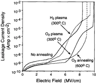
To further check the effect of plasma treatment on the properties of LPD oxide, the electrical char- acteristics of LPD oxide including I - V and inter- face-state were investigated. The typical I - V char- acteristics of LPD oxide films before and after plasma treatment for 1 h are shown in Fig. 2. The characteristics of the sample with 02 thermal an- nealing are also shown for comparison. The plasma-treated samples showed a lower leakage current at low electric field ( < 3 MV/cm) and a higher breakdown field than as-deposited and thermal annealed samples. In particular, the sample with the 02 plasma showed a much higher break- down field than that with H2 plasma. This phenom- enon was suspected to be due to less oxygen vacancies in the structure of 02 plasma-treated LPD oxide. That is, the LPD oxide with 02 plasma treatment had a denser structure and better atomic composition, and as a result exhibited better elec- trical characteristics. In comparison with O2 ther- mal annealing (600°C), the results also reveal that the 02 plasma treatment could effectively passivate the defects in LPD oxide film at low temperature. The histogram of breakdown field for the samples including as-deposited, 02 annealed, H2 plasma
10
-2
>,
10 -3"
,
"~t-
10-4- H 2 plasma f JI~ ~
(300°C) / ' /
|
0 ~ ~ Et~
lO-8-
No
anneali--I
~
-
~
-
~
02
annealing10 -9" ~
(600 ° C)
10-10
o lOElectric Field (MV/cm)
Fig. 2. J-E characteristics for the samples with and without plasma treatment and the sample with 02 thermal annealing at 600°C.
84 C.F. Yeh, S.S. Lin / Journal of Non-Crystalline Solids 187 (1995) 81-85 100. [ ] As-deposited 80. [ ] 0 2 annealing (600 ° C) ~ H 2 plasma (300 ° C) [ ] 02 plasma (300 ° C) o ~9 60. " - I • --~ 40. 20. o.~g~.'~. []. • . ., .I . . . 1 2 3 4 5 6 7 8 9 10 11
Breakdown Field (MV/cm)
Fig. 3. Breakdown field histogram for the LPD oxide with or
without plasma treatment and the sample with Oz thermal annealing at 600°C. 1013 1
10121
I-- -'- loll t : ¢- 1010 -0.4 %~ H a plasma (300°C) 02 plasma (a00°C) ~ -0'.2 0;0 O J2 0.4Bandgap Energy (eV)
Fig. 4. Interface state density distribution for the samples with and without plasma treatment and the sample with 02 thermal annealing at 600°C. Lines are drawn as guides for the eye.
a n d 0 2 plasma are shown in Fig. 3. We find that the 0 2 plasma-treated L P D oxide has a better distribution at high breakdown field than others.
To investigate the interface characteristics of L P D oxide after plasma treatment, the interface trap densities (Dit) for the samples after Oz o r H 2
plasma treatment were calculated by the Terman method [15]. As shown in Fig. 4, the interface trap
density was about 5 x 101~ eV t cm 2 for as-de- posited samples, while it was as low as 2 × 101° eV i c m - 2 for 0 2 plasma treated samples. The improvement of Dit at midgap was almost the same for the samples with 0 2 or Ha plasma treat- ment, and it is suspected that H or O could passi- vate the interface traps at midgap 1-16]. In addition, the reduction of Dit at the band edge by 0 2 plasma treatment was more obvious than that by H 2
plasma treatment. The interface traps near the band edge were attributed to be oxygen vacancies and weak Si-O bonds [17], so in 0 2 plasma treat- ment oxygen might diffuse into the films and reduce Dit near the band edge.
4. Summary
The physicochemical characteristics of L P D ox- ide films after plasma treatment exhibit great im- provement. They have higher refractive index and lower P-etch rates because they have denser struc- tures and less fluorine. The electrical characteristics also exhibited much improvement: there is a lower leakage current and higher breakdown field due to the passivation effect. The plasma treatment using 0 2 was more effective than using H 2. The plasma treatment also appeared superior to thermal an- nealing. Thus we conclude that plasma treatment is a more suitable method for improving the charac- teristics of L P D oxide films.
This work was supported by the National Science Council, Taiwan, under contract number NSC-83-0404-E-009-121.
References
[1] N. Nagayama, H. Honda and H. Kawahara, J. Elec- trocbem. Soc. 135 (1988) 2013.
[2] T. Goda, H. Nagayama, A. Hishinuma and H. Kawahara, Mater. Res. Sym. Proc. 105 (1988) 283.
[3] C.F. Yeh, S.S. Lin, C.L. Chern and Y.C. Yang, IEEE Electron Device Lett. EDL-14 (1993) 403.
[4] C.F. Yeh, S.S. Lin, T.Z. Yang, C.L. Chern and Y.C. Yang, IEEE Trans. Electron Devices ED-41 (1994) 173. r5] T. Horiuchi, K. Kanba, T. Homma, Y. Murao and K.
Okumura, IE, EE Trans. Electron Devices ED-40 (1993) 1455.
C.F. Yeh, S.S. Lin / Journal o f Non-Crystalline Solids 187 (1995) 81-85 85 [6] T. Homma, T. Katoh, Y. Yamada and Y. Murao, J. Elec-
trochem. Soc. 140 (1993) 2410.
[7] J. Lee, I.C. Chen and C. Hu, IEEE Electron Device Lett. EDL-7 (1986) 506.
[8] B.K. Ip, K.C. Kao and D.J. Thomson, Solid State Electron. 33 (1990) 123.
[9] M. Shyiang-Chyong Luo and C.T. Sah, Proc. Int. VLSI- TSA Conf. (1987).
[10] C.T. Sah, Solid State Electron. 33 (1990) 147.
[11] S. Yoshitomi, S. Tomioka and N. Haneji, Proc. 1992 Int. Electron Devices and Materials Syrup. (1992) p. 22.
[12] W.A. Pliskin, J. Vac. Sci. Technol. 14 (1977) 1064. [13] J.W. Fleming and D.L. Wood, Appl. Opt. 22 (1983) 3102. [14] J. Perriere, B. Pelloie, E. Fogarassy and A. Slaoui, Appl.
Surf. Sci. 29 (1987) 433.
[15] E.H. Nicollian and J.R. Brews, MOS (Metal Oxide Semiconductor) Physics and Technology (Wiley, New York, 1982).
[16] T. Sakurai and T. Sugano, J. Appl. Phys. 52 (1981) 2889. [17] H. Fukuda, M. Yasuda and T. Iwabuchi, J. Appl. Phys. 72