0167-9317/$ - see front matter Ó 2007 Elsevier B.V. All rights reserved. doi:10.1016/j.mee.2007.04.061
www.elsevier.com/locate/mee Microelectronic Engineering 84 (2007) 2077–2080
The impact of mobility enhanced technology on device
performance and reliability for sub-90nm SOI nMOSFETs
Wen-Kuan Yeh
Department of Electrical Engineering, National University of Kaohsiung, Taiwan, No. 700, Kaohsiung University Rd., Nan-Tzu Dist., Kaohsiung, Taiwan
Abstract
For SOI nMOSFET, the impact of high tensile stress contact etch stop layer (CESL) on device performance and reliability was investigated. In this work, device driving capability can be enhanced with thicker CESL, larger LOD and narrower gate width. With electrical and body potential inspection, serious device’s degradation happened on SOI-MOSFET with narrow gate device because of STI-induced edge current.
Keywords: Contact etch stop layer; STI-induced edge current
1. Introduction
High stress SiN layer have been adapted for the mobility improvement of MOSFETs [1-3]. For nMOSFETs, the high tensile stress caused by contact etch stop layer (CESL) is the major factor of mobility improvement. However, shallow trench isolation will induce compressive stress to compete with this CESL-induced tensile stress. There are few reports studying the interactive stress effect between CESL SiN film and device geometry especially for SOI device. In this work, the impact of CESL thickness, gate width and length of diffusion (LOD) on device
Corresponding author. Tel.: +886-7-5919234; fax: +886-7-5919374
E-mail address: wkyeh@nuk.edu.tw (W.-K. Yeh)
performance and hot-carrier induced degradations for 90nm partially depleted (PD-SOI) nMOSFETs were inspected. For SOI MOSFET with floating body effect, body potential investigation was used to understand these interactions.
2. Experimental
PD-SOI nMOSFETs devices on IMplanted OXygen (SIMOX) <100> channel orientation SOI substrate were fabricated with a 40 nm Si active layer and 200 nm buried oxide (BOX). The PD-SOI device with body contact (BC-SOI) or without (FB-SOI: with floating body effect) was formed with various thicknesses of high stress CESL, LOD and gate width were prepared. A direct current (DC) measurements were carried out under various drain voltages
2078 W.-K. Yeh / Microelectronic Engineering 84 (2007) 2077–2080
(VD = 0~1.4 V) and gate voltages (VG= 0~1.4 V),
hot-carrier stressing was performed with VG=VD=1.2
V under room temperature (25 oC) for 100 min. Body potential of FB-SOI MOSFET can be monitored by BC-SOI MOSFET with zero body current.
3. Results and discussion
The device structure was shown in Fig. 1(a), which indicates the orientations of stress caused by CESL and shallow trench isolation (STI). In x axis, the CESL will induce a tensile stress in channel region, and a compressive stress can be caused by STI surrounded the whole device, as shown in Fig. 1(b). It is clearly that the amount of compressive stress in y axis is related to the gate width and those in x axis are related to the length of LOD. The channel tensile stresses induced by CESL will enhance the channel carrier mobility, further improving device’s driving capability especially for device with thicker CESL, as shown in Fig. 2.
Fig. 1. The stress items in MOSFET channel region.
However, we found that thick CESL will also induced more damages especially in device channel region, resulting in device degradation. Thus, the thickness of CESL for efficient improvement in device performance needs to be optimized. In this work, 700A CESL device can improve device’s driving capability more efficient than 1100A one does. It is presumably that higher trapped charges in Si/SiO2 were found on 1100A CESL device due to
inappropriate higher stress, thus resulting in higher
threshold voltage shift and degrading device’s driving capability.
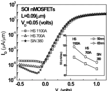
For sub-90nm device, Fig. 3 shows devices with 1100A CESL possess larger gate induced drain leakage (GIDL) and subthreshold swing. An input-referred noise spectrum of FB-SOI nMOSFETs with various CESL was shown in Fig. 4.
0.0 0.5 1.0 1.5 0 200 400 600 800 1000 1200 1400 nMOS FB-SOI L / W = 0.09 / 10Pm VG=1.4 V
high stress 1100A high stress 700A SiN 380 VD (volts) ID ( P A/ P m) 0 200 400 600 800 1000 1200 ID ( P A/ P m) nMOS BC-SOI L / W = 0.09 / 10Pm VG=1.4 V
high stress 1100A high stress 700A SiN 380
(a)
(b)
0.0 0.5 1.0 1.5 0 200 400 600 800 1000 1200 1400 nMOS FB-SOI L / W = 0.09 / 10Pm V G=1.4 Vhigh stress 1100A high stress 700A SiN 380 VD (volts) ID ( P A/ P m) 0 200 400 600 800 1000 1200 ID ( P A/ P m) nMOS BC-SOI L / W = 0.09 / 10Pm VG=1.4 V
high stress 1100A high stress 700A SiN 380
(a)
0.0 0.5 1.0 1.5 0 200 400 600 800 1000 1200 1400 nMOS FB-SOI L / W = 0.09 / 10Pm V G=1.4 Vhigh stress 1100A high stress 700A SiN 380 VD (volts) ID ( P A/ P m) 0 200 400 600 800 1000 1200 ID ( P A/ P m) nMOS BC-SOI L / W = 0.09 / 10Pm VG=1.4 V
high stress 1100A high stress 700A SiN 380
(a)
0 200 400 600 800 1000 1200 ID ( P A/ P m) nMOS BC-SOI L / W = 0.09 / 10Pm VG=1.4 Vhigh stress 1100A high stress 700A SiN 380
(a)
(b)
Fig. 2. ID-VD of 90 nm (a) BC-SOI (b) FB-SOI nMOSFETs with various stress CESL liner- SiN thicknesses.
-0.5 0.0 0.5 1.0 10-7 10-5 10-3 10-1 101 103 60 80 100 120 140 SiN 380 HS 700A HS 1100A SS ( m V /de c) 90nm 65nm ID ( P A/ P m) SOI nMOSFETs L=0.09(Pm) VD=0.05 (volts) HS 1100A HS 700A SiN 380 VG (volts)
Fig. 3. ID-VG of SOI nMOSFETs with various stress CESL liner-SiN layers. The insert shows device’s subthreshold swing.
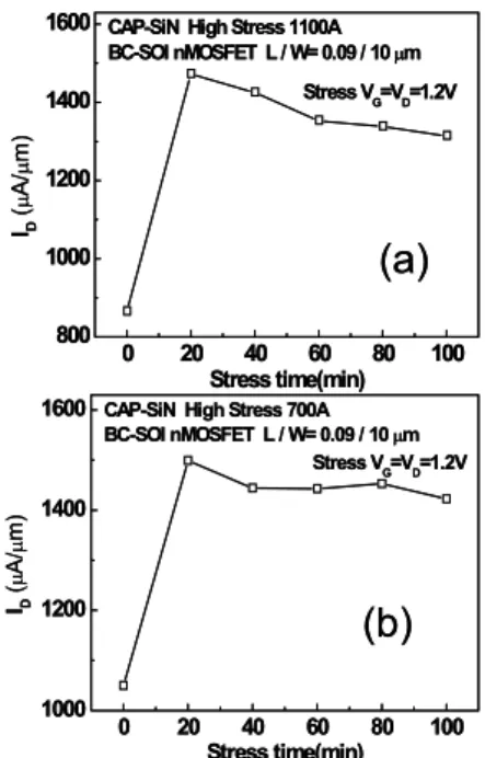
Owing to higher drain body junction leakage can be caused by interface defect, thus larger Lorentzian-like noise overshoot [3] will happened on device with thicker CESL. Fig. 5 shows the driving capability degradation of 90 nm BC-SOI nMOSFETs
W.-K. Yeh / Microelectronic Engineering 84 (2007) 2077–2080 2079
with different CESLs after 100 min hot-carrier stressing, respectively. Apparent shift of device’s ID
rises apparently just after hot-carrier stressing first (Fig. 5(a)) and then device degrades finally. Compared with 1100A device which will induce inappropriate high tensile stress and serious damage, less deviation of device drain current (ID) degradation
was found on 700A SiN device (Fig. 5(b)). Similar tendency was found on device’s Gm degradation. For
the interaction between CESL film (tensile) and STI
edge (compressive), the ǻID versus device gate width
for 90 nm FB-SOI nMOSFETs with various CESL was shown in Fig. 6. (Ref. ID = 735 ȝA/ȝm @
devices with W = 10ȝm, LOD = 0.45 ȝm and 1100A CESL).
Compared with devices with wider width=10ȝm, it is apparent that IDincreases as the LOD increases.
It is well known that device with STI show an inverse-narrow-width effect caused by fringing electric fields [4], enhancing the channel edge current; therefore, the total current density ID increases as the
gate width reduces. Thus, the effect of LOD in narrow width device was no apparent on device’s performance because of the large edge current has overtaken the benefit of LOD effect.
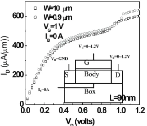
Fig. 6 shows that larger channel edge current will happen on narrow width devices, resulting in severe the hot-carrier induced device degradations. In this work, a method which setting BC-SOI device with IB= 0 A was used to monitor the body potential (VB)
of FB-SOI device, as shown in inset of Fig. 7.
0 100 200 300 0 1 2 3 4 5
Stress time (min)
W=1.2 Pm W=5 Pm W=10 Pm Stress Voltage: V G=VD=1.5V L=90nm ' IDsa t (% )
Fig. 6. IDsat degradation vs. stress time for 90 nm SOI nMOSFETs with different gate width.
Fig. 7 shows that a kink effect will happen on BC-SOI nMOSFETs with IB= 0 A; thus, we believed
it is a reasonable way to monitor the characteristic of FB-SOI devices. Fig. 8 shows that the channel mobility of nMOSFET will increase as channel width decrease for both SOI devices. It is apparently that larger STI-induced edge leakage happens especially on device with narrow width, resulting in device driving capability degradation. With a body potential inspection, Fig. 9 shows that lower VB was found at
narrower width device especially at large VD due
presumably to gate induce drain leakage (GIDL) happened. Apparently, lower VB can be found in
101 102 103 104 105 10-14 10-13 10-12 10-11 10-10 10-9 f0:HS 1100A f0:HS 700A f0:SiN 380 SiN 380 HS: 700A HS: 1100A FB-SOI nMOSFETs L/W=0.18/10Pm VD=0.05 V VG=1.2 V SVG (V 2/ H z ) Frequency (Hz)
Fig. 4. Input-referred noise spectra of FB-SOI nMOSFETs in linear region. GR noise was happened early on con- ventional SiN device at device operating exceed 300 kHz.
0 20 40 60 80 100 1000 1200 1400 1600 Stress VG=VD=1.2V CAP-SiN High Stress 700A
BC-SOI nMOSFET L / W= 0.09 / 10 Pm ID ( P A/ P m) Stress time(min) 0 20 40 60 80 100 800 1000 1200 1400
1600 CAP-SiN High Stress 1100A BC-SOI nMOSFET L / W= 0.09 / 10 Pm Stress VG=VD=1.2V ID ( P A/ P m) Stress time(min)
(a)
(b)
0 20 40 60 80 100 1000 1200 1400 1600 Stress VG=VD=1.2V CAP-SiN High Stress 700ABC-SOI nMOSFET L / W= 0.09 / 10 Pm ID ( P A/ P m) Stress time(min) 0 20 40 60 80 100 800 1000 1200 1400
1600 CAP-SiN High Stress 1100A BC-SOI nMOSFET L / W= 0.09 / 10 Pm Stress VG=VD=1.2V ID ( P A/ P m) Stress time(min)
(a)
(b)
Fig. 5. Stress-induced ID and GM (inset) degradation of 90 nm BC-SOI nMOSFET with (a) 1100A (b) 700A high stress CESL liner-SiN.
2080 W.-K. Yeh / Microelectronic Engineering 84 (2007) 2077–2080
especially narrower width device with larger STI-induced edge leakage, as shown in Fig. 10. By the way, the body potential is more sensitive with gate voltage because larger gate tunneling happens at larger gate bias.
Fig. 7. ID-VD characteristics of 90 nm BC-SOI nMOSFETs with different gate width and IB = 0 A. The insert shows the measurement setup. -0.4 0.0 0.4 0.8 0 200 400 600 800 1000 1200 VD=1 V VG- Vth (Volts) Gm / W ( S / P m) W=10 Pm W=10 Pm, IB=0 A W=3.6 Pm W=3.6 Pm, IB=0 A W=0.9 Pm W=0.9 Pm, IB=0 A
Fig. 8. Width effect on Gm of 90nm BCSOI nMOSFETs with IB = 0 A or not.
4. Conclusions
In this work, the interaction between CESL film thickness, LOD and gate width impact on SOI nMOSFET performance and hot-carrier induced device degradation was investigated. We found that devices with 700A CESL possess efficient mobility enhancement and hot-carrier reliability immunity than devices with 1100A CESL do. Owing to inappropriate high tensile stress, thicker CESL will induce large stress defects, thus degrading device characteristics. Increasing the LOD distance will decrease the STI-induced compressive stress and
enhance the channel mobility, enhancing device’s driving capacity. Owing STI-induced edge current, narrow width device possess lower body potential, which causing larger drain current and increases the hot-carrier induced device degradations as the gate width reduces.
Acknowledgements
The authors would like to thank the staff members of UMC Advanced Device department for their helpful comments. The National Science Council of Taiwan, R.O.C., under Contract NSC 96-2221-E-390- 028, supported this work.
References
[1] T. Komoda, A. Oishi, T. Sanuki, A. Iwai, M. Saito, F. Matsuoka, N. Nagashima, T. Noguchi, IEEE IEDM Tech. Dig. 2004, 217-220.
[2] S. E. Thompson, M. Armstrong, C. Auth, M. Alavi, M. Buehler, R. Chau, S. Cea, T. Ghani, G. Glass, T. Hoffman, et. al., IEEE TED 51 (2004) 1790-1797. [3] S. Pidin, T. Mori, R. Nakamura, T. Saiki, R. Tanabe,
Satoh, S. T. Sugii, VLSI Symp. Tech. Dig. 6(2004) 54.
0.0 0.2 0.4 0.6 0.8 1.0 1.2 0.0 0.1 0.2 0.3 0.4 0.5 L =90nm VG=1V VB (v olts) VD (volts) W=10 Pm W=0.9 Pm W=0.45 Pm W=0.18 Pm
Fig. 9. Width effect on VB-VD behavior of 90 nm BC-SOI nMOSFETs with IB = 0 A. -0.4 0.0 0.4 0.8 1.2 -0.1 0.0 0.1 0.2 0.3 0.4 0.5 L =90nm VD=1V W=10 Pm W=0.9 Pm W=0.45 Pm W=0.18 Pm VG (volts) VB (v o lt s )
Fig. 10. Width effect on VB-VG behavior of 90 nm BC-SOI nMOSFETs with IB= 0 A.