國立交通大學
顯示科技研究所
碩士論文
具保護層之非晶態銦鎵鋅氧薄膜電晶體
穩定性研究
Stabilization of Amorphous Indium-Gallium-Zinc
Oxide Thin Film Transistors by a Passivation Layer
研究生: 陳泳材
指導教授: 謝漢萍 教授
具保護層之非晶態銦鎵鋅氧薄膜電晶體
穩定性研究
Stabilization of Amorphous Indium-Gallium-Zinc
Oxide Thin Film Transistors by a Passivation Layer
研究生: 陳泳材
Student: Yung-Tsai Chen
指導教授: 謝漢萍
Advisor: Han-Ping D. Shieh
國立交通大學 電機學院
顯示科技研究所
碩士論文
A Thesis
Submitted to Display Institute
College of Electrical and Computer Engineering
National Chiao Tung University
in Partial Fulfillment of the Requirements
for the Degree of Master
in
Display Institute
June 2010
Hsinchu, Taiwan,
Republic of China
中華民國 九十九 年 六 月
i
具保護層之非晶態銦鎵鋅氧薄膜電晶體
穩定性研究
碩士研究生:陳泳材
指導教授 謝漢萍 教授
國立交通大學 顯示科技研究所
摘 要
透明非晶態銦鎵鋅氧化物的載子遷移率已超越使用在液晶螢幕面板中的非晶態矽, 並實現透明電子產品。與環境的水氧反應和偏紫外光波段波長的吸收造成非晶態銦鎵鋅 氧薄膜電晶體的不穩定性,在商品化的過程將是一個重大的議題。本論文藉由加入一層 通道保護層降低非晶態銦鎵鋅氧與外界反應的機會,利用濺鍍方式沉積氧化矽和氮化矽 為通道保護層,首先探討通道保護層對非晶態銦鎵鋅氧薄膜電晶體的元件特性影響;進 一步研究具通道保護層的元件放置環境中與在照光的情況下,臨界電壓隨時間變化有穩 定的效果。此外對非晶態銦鎵鋅氧薄膜電晶體給予直流偏壓測試,發現具通道保護層的 元件有較佳的可靠度。從薄膜特性、電性的穩定度與元件的可靠度比較,結果指出氮化 矽比氧化矽適合當通道保護層。:
ii
Stabilization of Amorphous Indium-Gallium-Zinc Oxide Thin
Film Transistors by a Passivation Layer
Master Student: Yung-Tsai Chen
Advisor Dr. Han-Ping D. Shieh
Display Institute
National Chiao Tung University
Abstract
The discovery of transparent oxides with high mobility realizes the transparent electronics and is being used for LCD backplane. The electrical instability of amorphous indium-gallium-zinc oxide (IGZO) thin film transistors is caused by two mechanisms:the interaction of oxygen and moisture in the ambience and the absorption of the light in near-ultraviolet region. To be electronic products, the electrical stability is a key issue. In the thesis, we studied on the sputtered SiOx and SiNx which serve as the passivation layer on the back channel to prevent the a-IGZO films from interacting with the ambience. First, film properties of the passivation layer are investigated and the effect of the passivation layer on the back channel of a-IGZO TFT is discussed. Further, the passivated devices with a stable threshold voltage as the function of time in the ambience and under light illumination are studied. The passivated a-IGZO TFTs present an improved reliability in comparison with the unpassivated devices under DC bias stress. By comparing the properties of the passivation layer, the electrical stability, and the device reliability, SiNx is found to be more suitable than SiOx as passivation for higher density in the structure and lower threshold voltage shift in the electrical properties.
iii
誌謝
能夠順利完成本篇論文,首先要感謝謝漢萍教授為我們建立了一個資源豐富的研究 環境,讓我的碩班生涯著實受益良多,實驗室注重英文能力也讓我們不忘踏出關門研究 的階段,培養國際化的視野,成為更全方位的人才,更從教授身上學習到正確待人處事 的方法,在此致上最誠摯的謝意。 也很感謝韻竹學姐,益興學長,高銘學長,提供許多寶貴的意見,不僅引導我在研 究上突破瓶頸,更令我從挫折當中學習到該有的學習態度。在實驗的過程中我最感謝我 的好夥伴耆賢。他與我在無塵室內,共度無數時光。另外,要謝謝同樣在無塵室內的其 他實驗室夥伴們,在研究上給我許多的鼓舞支持,也在閒暇之餘帶給我許多歡樂。 此外,也很感謝世勛,期竹,姚順,毅瀚,裕閔,甫奕,怡菁,景文,以及壁丞, 和你們這些夥伴一起奮鬥的日子,是我一輩子珍惜的回憶。也很謝謝實驗室的學長姐以 及學弟妹們,有你們的陪伴,替碩士生涯添增樂趣。 最後,要謝謝我的家人,因為有你們的支持與付出,也因為有你們的教導,我才能 夠順利完成碩士學業。謝謝我家人對我付出的一切,謹以本文獻給家人和關懷我的人。iv
Table of Contents
Abstract(Chinese) ... i
Abstract(English) ... ii
Acknowledge ... iii
Table of Contents ... iv
Figure Captions ... vii
List of Tables ... xi
Chapter 1 ... 1
1.1 General Background ... 1
1.2 Oxide Semiconductors ... 3
1.3 Amorphous In-Ga-Zn-O Thin Film Transistors ... 5
1.3.1 Introduction of a-IGZO TFTs ... 5
1.3.2 The In2O3-Ga2O3-ZnO Ternary System ... 8
1.3.3 The Issue and Prior Art of a-IGZO TFTs for Stability ... 10
1.4 Motivations and Objectives ... 11
1.5 Organization of this Thesis ... 12
Chapter 2 ... 13
2.1 Introduction ... 13
2.2 The Operation Principle of Thin Film Transistor ... 13
2.3 The Method of Parameter Extraction ... 16
2.4 Origin of Instability in a-IGZO TFTs... 18
2.4.1 The Behavior of a-IGZO TFTs in the Ambience ... 18
v
2.4.3 The Mechanism of a-IGZO TFTs in Voltage Stress ... 19
2.5 The Mechanism of Gas Permeation ... 21
2.6 Summary ... 22
Chapter 3 ... 23
3.1 Introduction ... 23
3.2 Process Design and Schemes ... 23
3.3 Materials and Instruments ... 24
3.4 The Fabrication Process of a-IGZO TFTs ... 26
3.5 The Principle of Sputtering ... 31
3.6 Devices Measurement and Analysis ... 32
3.7 Summary ... 37
Chapter 4 ... 38
4.1 Introduction ... 38
4.2 Analysis of the Passivation Layer... 38
4.2.1 Film Morphology Analysis ... 38
4.2.2 Cross-section Observation ... 42
4.2.3 Moisture Content ... 44
4.2.4 Contact Angle Measurement ... 45
4.2.5 Transmittance ... 45
4.3 Electrical Characteristics Analyses of Passivated a-IGZO TFTs ... 47
4.3.1 The a-IGZO TFTs Before and After Deposited SiOx as Passivation ... 47
4.3.2 The a-IGZO TFTs Before and After Deposited SiNx as Passivation ... 47
4.3.3 Discussion ... 48
vi
4.4.1 Analyses of Passivated a-IGZO TFTs in the Ambience ... 52
4.4.2 Analyses of Passivated a-IGZO TFTs under Illumination ... 60
4.5 Reliability of Passivated a-IGZO TFTs ... 68
4.6 Summary ... 73
Chapter 5 ... 74
5.1 Conclusions... 74
5.2 Future Works ... 75
vii
Figure Captions
Fig. 1-1 Schematic of active matrix... 2
Fig. 1-2 Cross section of a pixel in a TFT LCD. ... 3
Fig. 1-3 The structure of the active layer... 3
Fig. 1-4 Schematic orbital drawing of electron pathway in (a) covalent semiconductors and (b) metal oxide semiconductors, respectively [1]. ... 5
Fig. 1-5 Transmittance of a-IGZO in visible light. [14] ... 6
Fig. 1-6 The display image of Samsung’s 12.1 inch WXGA AMOLED display. [15] ... 7
Fig. 1-7 The photo of the lecture delivered by AUO... 7
Fig. 1-8 The amorphous formation region (right) and the electron mobility and concentrations evaluated from the Hall effects for the amorphous thin films (left) in the In2O3–Ga2O3–ZnO system, respectively. The thin films were deposited on a glass substrate by pulse laser deposition under deposition atmosphere of PO2 = 1 Pa. Number in the parenthesis denotes carrier electron concentration (x1018 cm-3). [1] . 9 Fig. 1-9 The carrier concentration as a function of O2 pressure during the deposition in a-IGZO and a-IZO. [1] ... 9
Fig. 1-10 Schematic view of a-IGZO TFTs with passivation. ... 12
Fig. 2-1 Schematic view of (a) top contact and (b) bottom contact TFTs, respectively……...15
Fig. 2-2 The semiconductor energy band diagram when (a) unbiased, (b) negative gate voltage bias, and (c) positive gate voltage bias, respectively. ... 15
Fig. 2-3 Schematic of TFTs operation in accumulation mode: (a) unbiased, (b) negative gate voltage bias, and (c) positive gate voltage bias, respectively. ... 15
Fig. 2-4 The schematic diagram showing the role of (a) oxygen as an electron acceptor and (b) water molecules as a electron donor onto a-IGZO surface, respectively. [19] ... 20
Fig. 2-5 (a) Band diagram of a-IGZO TFTs operated under illumination and (b) closer look at the channel region, respectively. ... 20
Fig. 2-6 Energy band diagram of a-IGZO TFTs (a) electron injection and trapping within the gate insulator, (b) deep state creation and (c) electron trapping within the a-IGZO channel layer, respectively. [28] ... 21
Fig. 2-7 Solution-diffusion model. [30] ... 22
Fig. 3-1 Flowchart of the study. ... 24
Fig. 3- 2 The flow chart of a-IGZO TFTs device fabrication... 28
viii
Fig. 3-4 Thermal evaporation system in NCTU. ... 29
Fig. 3-5 Tube furnace in NCTU. ... 30
Fig. 3-6 The photograph of fabricated devices. ... 30
Fig. 3-7 Schematic of RF sputtering system. ... 31
Fig. 3-8 A schematic model of AFM. ... 33
Fig. 3-9 A schematic of SEM. ... 33
Fig. 3-10 The contact angle formation of liquid on solid surface. ... 34
Fig. 3-11 The construction of Karl Fischer moisture titrator. ... 35
Fig. 3-12 A schematic of Ultraviolet-visible spectroscopy. ... 36
Fig. 4-1 Growth steps of film: (a) the nucleation, (b) the diffusion, and (c) the coarsening step, respectively. [31] ... 39
Fig. 4-2 SEM image of (a) the SiOx film and (b) the SiNx film deposited by sputtering, respectively. ... 40
Fig. 4-3 AFM morphology of (a) the SiOx film and (b) the SiNx film deposited by sputtering, respectively. ... 41
Fig. 4-4 The cross section image of (a) the SiOx film and (b) the SiNx film deposited by sputtering, respectively. ... 43
Fig. 4-5 The moisture content of the three samples included the a-IGZO film, the a-IGZO film with SiOx as passivation, and the a-IGZO film with SiNx as passivation measured by Karl Fischer moisture titrator, respectively... 44
Fig. 4-6 Contact angle for DI water drop on the (a) SiOx and (b) SiNx film deposited by sputtering, respectively. ... 46
Fig. 4-7 The transmittance of the SiOx and SiNx film deposited by sputtering. ... 46
Fig. 4-8 ID-VG curves of a-IGZO TFTs before and after deposited SiOx as passivation. ... 50
Fig. 4-9 ID-VD curves of a-IGZO TFTs before and after deposited SiOx as passivation. ... 50
Fig. 4-10 ID-VG curves of a-IGZO TFTs before and after deposited SiNx as passivation. ... 51
Fig. 4-11 ID-VD curves of a-IGZO TFTs before and after deposited SiNx as passivation. ... 51
Fig. 4-12 (a) A device structure: b.i. represents the back interface region and f.i. is the front interface region. (b) The surface band banding profile and the current density for various gate voltage at VDS=10 V. [33] ... 52
Fig. 4-13 ID-VG curves of a-IGZO TFTs without passivation in the ambience. ... 56
Fig. 4-14 Threshold voltage of a-IGZO TFTs without passivation in the ambience as the function of time (days). ... 56
ix
Fig. 4-15 ID-VG curves of a-IGZO TFTs with SiOx as passivation in the ambience. ... 57 Fig. 4-16 Threshold voltage of a-IGZO TFTs with SiOx as passivation in the ambience as the
function of time (days). ... 57 Fig. 4-17 ID-VG curves of a-IGZO TFTs with SiNx as passivation in the ambience. ... 58 Fig. 4-18 Threshold voltage of a-IGZO TFTs with SiNx as passivation in the ambience as the
function of time (days). ... 58 Fig. 4-19 Contact angle image for de-ionized water drop on the a-IGZO film for (a) initial
state and (b) the state of exposed to the ambience in ten days, respectively. ... 59 Fig. 4-20 Threshold voltage of a-IGZO TFTs dipped in the water as the function of time
(hours). ... 59 Fig. 4-21 ID-VG curves of a-IGZO TFTs without passivation in the dark, under illumination,
and after switching off the light, respectively. ... 63 Fig. 4-22 ID-VG curves of a-IGZO TFTs without passivation in the dark and after switching
off the one minute light illumination. ... 64 Fig. 4-23 Threshold voltage of a-IGZO TFTs without passivation under illumination. ... 64 Fig. 4-24 ID-VG curves of a-IGZO TFTs with SiOx as passivation in the dark, under
illumination, and after switching off the light, respectively. ... 65 Fig. 4-25 ID-VG curves of a-IGZO TFTs with SiOx as passivation in the dark and after
switching off the one minute light illumination. ... 65 Fig. 4-26 Threshold voltage of a-IGZO TFTs with SiOx as passivation under illumination. .. 66 Fig. 4-27 ID-VG curves of a-IGZO TFTs with SiNx as passivation in the dark, under
illumination, and after switching off the light, respectively. ... 66 Fig. 4-28 ID-VG curves of a-IGZO TFTs with SiNx as passivation in the dark and after
switching off the one minute light illumination. ... 67 Fig. 4-29 Threshold voltage of a-IGZO TFTs with SiNx as passivation under illumination. .. 67 Fig. 4-30 ID-VG curves of a-IGZO TFTs without passivation in voltage stress. ... 70 Fig. 4-31 ID-VG curves of a-IGZO TFTs with SiOx as passivation in voltage stress. ... 70 Fig. 4-32 ID-VG curves of a-IGZO TFTs with SiNx as passivation in voltage stress. ... 71 Fig. 4-33 The threshold voltage shift of a-IGZO TFTs without passivation, with SiOx, and
with SiNx as passivation in voltage stress, respectively... 71 Fig. 4-34 The threshold voltage shift of a-IGZO TFTs without passivation, without
passivation in the vacuum, with SiOx, and with SiNx as passivation in voltage stress, respectively. ... 72
x
Fig. 4-35 Normalized (I/I0) drain current degradation as the function of time (s). ... 72 Fig. 5-1 The scheme of a-IGZO TFT device deposited by sputtering. ... 76
xi
List of Tables
Table 1-1 The prior arts of a-IGZO TFTs with passivation ... 11
Table 3-1 Experimental materials ... 25
Table 3-2 Measurement instruments ... 25
Table 3-3 Fabrication instruments ... 26
Table 4-1 Contact angle of the SiOx and the SiNx film deposited by sputtering ... 46
Table 4-2 Comparison of device performances before/after deposited SiOx and SiNx as passivation ... 48
Table 4-3 Device performances without passivation, with SiNx as passivation, and with SiNx as passivation, respectively, in the ambience ... 54
Table 4-4 Contact angle of the a-IGZO film for initial state and the state of exposed to the ambience in ten days ... 59
Table 4-5 Device performances without passivation, with SiOx as passivation, and with SiNx as passivation in the dark and after switching off the one minute light illumination, respectively. ... 62
1
Chapter 1
Introduction
1.1 General Background
Thin film transistors (TFTs) have been widely employed as the pixel-driving elements for flat panel display, such as active-matrix liquid crystal display (AMLCD) and active matrix organic light emitting diode (AMOLED). The performance of active matrix TFTs backplane is dependent on at least two factors: the individual pixels and the interconnection lines. Generally, an active matrix TFTs backplane is composed of an array of pixels connected with vertical and horizontal programming lines. Fig. 1-1 shows the schematic of active matrix. Scan lines are connected to gates of switching TFTs of the pixels, data lines are used to drive TFTs sources, and drains are connected to the liquid crystal (LC). Fig. 1-2 shows the cross section of a pixel in a TFT LCD. Each pixel includes polarizer, TFTs devices, spacer, liquid crystal, alignment layer and color filter, etc. TFTs devices can be roughly divided into two types by the crystal structure of active layer: amorphous state and crystal state as shown inFig. 1-3. The field effect mobility of amorphous silicon (a-Si) is quite low compared to poly-crystal silicon (poly-Si) due to its messy amorphous state. In practical applications, poly-Si TFTs are suitable for the small size flat panel display because of the grain boundary. On the other hand, the a-Si TFTs are often applied in large size flat panel display on account of its mature manufacture and low fabrication cost. The drawbacks of a-Si include visible light sensitivity and low field-effect mobility, which reduce the pixel aperture ratio and driving ability. Besides, a new electronics is emerging for applications which cannot be fabricated by silicon metal oxide semiconductor (MOS) technology. Recently, metal oxide
2
semiconductor based TFTs have attracted much attention for future applications such as flexible and transparent displays [1,2,3].This is due to unique electrical and optical properties of metal oxide semiconductor based TFTs which are transparent in visible light, good large-area uniformity deposition at low process temperature, and high field effect mobility. In particular, the resistivity of metal oxide semiconductor can be turned from insulator to metal by controlling the oxygen partial pressure, which produces prospective markets for industries such as oxide electronics and transparent displays [4].
3
Fig. 1-2 Cross section of a pixel in a TFT LCD.
Fig. 1-3 The structure of the active layer.
1.2 Oxide Semiconductors
The thin film metal oxide materials such as SnO2, In2O3, ZnO, CdO and their alloys have visible light transparency and high electrical conductivity [5]. In particular, indium tin oxide (ITO) is well known to the display industry. These metal oxide materials can also have
4
semi-conductive property to be used as the active layer of TFTs [6].
In recent year, these metal oxide TFTs have been reported to exhibit field effect mobility above 10 cm2/Vs even in the amorphous state, which is more than one order of magnitude compared to traditional a-Si TFTs [7,8]. The mobility of a-Si:H TFTs is limited to around 1 cm2/Vs which is associated with the intrinsic nature of the chemical bonding. Fig. 1-4 (a) illustrates average carrier transport paths in covalent semiconductors such as a-Si:H which is consist of sp3 orbital with strong directivity. The bond angle fluctuation significantly alters the electronic levels, causing the high density traps deep of tail-states. In contrast, metal oxide semiconductors contained post transition metal cations with the (n-1)d10ns0 electron configuration, where n ≥ 5, have large mobility (>10 cm2
/Vs) [2]. Fig. 1-4 (b) illustrates the carrier transport path in metal oxide semiconductors which are composed of spatially spread ns orbital with an isotropic shape, where the ns orbital overlap among the neighbouring orbital directly. The isotropic of the ns orbital is insensitive to the disorder structure which intrinsically exists in amorphous materials that can avoid significant degradation of transport properties [9]. This feature shows why the field effect mobility of amorphous metal oxide semiconductors is similar to the corresponding crystalline phase, even under the room temperature deposition process. The amorphous metal oxide semiconductor based TFTs can be one of the promising candidates for the increase in the size of the flat panel display because of high mobility and good uniformity.
Zinc oxide (ZnO) is a conventional metal oxide semiconductor which is polycrystalline state in nature even at room temperature. The grain boundaries of such metal oxides affect device properties, uniformity and stability over large areas. Although, the ZnO-based semiconductors such as In-Zn-O, Zn-Sn-O and In-Ga-Zn-O can be amorphous state at room temperature and have been proposed as the active layer in TFTs [10,11,12]. These amorphous ZnO-based TFTs overcome the drawbacks of a-Si:H and poly-Si TFTs in flat panel displays.
5
Fig. 1-4 Schematic orbital drawing of electron pathway in (a) covalent semiconductors and (b) metal oxide semiconductors, respectively [1].
1.3 Amorphous In-Ga-Zn-O Thin Film Transistors
1.3.1 Introduction of a-IGZO TFTs
One of the interesting oxide semiconductors for TFTs applications is a ternary material composed of In2O3、Ga2O3 and ZnO named IGZO. Hosono et. al. have proposed the high performance TFTs using a-IGZO deposited on plastic substrates by pulse laser deposition at room temperature as the active layer [10]. The performance of a-IGZO TFTs is also confirmed by using the sputter deposition [7], which demonstrates the possibility of the large area applications. In addition, the a-IGZO is transparent to visible light due to its optical energy
6
band gap of about 3eV [13]. Fig. 1-5 shows the transmittance is greater than 80 percent from 400 nm to 850 nm wavelength [14]. Hence a-IGZO TFTs are useful for new applications such as transparent displays.
Fig. 1-5 Transmittance of a-IGZO in visible light. [14]
The a-IGZO has considered favorable material for practical TFTs such as liquid crystal displays (LCDs) and organic light-emitting diode (OLED) displays. Consequently, the a-IGZO TFTs technology is rapidly expanding to more practical prototypes such as 12.1 inch AMOLED and 15 inch AMLCD high-resolution displays [15,16]. In SID 2008, a full color 12.1 inch WXGA AMOLED display using a-IGZO TFTs as an active-matrix backplane was demonstrated by Samsung, as shown in Fig. 1-6. The a-IGZO TFTs exhibited the field-effect mobility (μ) of 8.2 cm2
/Vs, threshold voltage (Vth) of 1.1 V, Ion/Ioff around 108, and subthreshold swing (S.S.) of 0.58 V/decade.
7
Fig. 1-6 The display image of Samsung’s 12.1 inch WXGA AMOLED display. [15]
In SID 2010, a full-HD (1,920 x 1,080 pixels) 37-inch LCD panel based on a transparent a-IGZO semiconductor was demonstrated by AU Optronics Corporation, as shown in Fig. 1-7. The coplanar type of a-IGZO TFTs with gate width and length are 22 and 5 μm, respectively, exhibited the field-effect mobility (μ) of 10 to 13 cm2/Vs and Ion/Ioff higher than 108.
8
1.3.2 The In
2O
3-Ga
2O
3-ZnO Ternary System
For the In2O3-Ga2O3-ZnO ternary system, the mobility can be changed by choosing different chemical composition [17,18]. Fig. 1-8 shows the relationship among chemical composition, mobility and carrier concentration in a-IGZO thin film by pulse laser deposition at room temperature. It is clear that higher value of mobility is obtained around the samples containing more In2O3 fraction. In contrast, incorporation of Ga decreases carrier concentration and mobility.
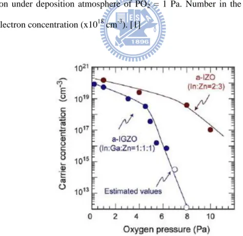
The largest mobility of 39 cm2/Vs is obtained in a-IZO with the carrier concentration of 1×1020 cm-3. For good TFTs operation, a-IZO has a high carrier concentration. In practice, the effect of binary amorphous materials in the In2O3–ZnO system is employed in commercial flexible transparent conductive films by depositing on the plastic sheet. The carrier concentration of amorphous metal oxide materials is related to oxygen vacancies. Thus, the effect of partial oxygen pressure was studied during the deposition processes on the carrier concentration in a-IGZO and a-IZO, the results are shown in Fig. 1-9. The carrier concentration in the a-IGZO is distinctly reduced to below 1013 cm-3 by increasing PO2 to 8 Pa. Nevertheless, the carrier concentration of a-IZO remains at 1018 cm-3 under the same condition. The result indicates the incorporation of Ga is effective to suppress the electron carrier generation. Ga3+ is supposed to attract the oxygen ions tightly due to its small ionic radius causing high ionic potential, and thereby suppressing electron injection which is caused by oxygen ion escaping from the thin film. This is why a-IGZO has been widely researched as active layer for TFTs instead of a-IZO which has the higher mobility.
9
Fig. 1-8 The amorphous formation region (right) and the electron mobility and concentrations evaluated from the Hall effects for the amorphous thin films (left) in the In2O3–Ga2O3–ZnO system, respectively. The thin films were deposited on a glass substrate by pulse laser deposition under deposition atmosphere of PO2 = 1 Pa. Number in the parenthesis denotes carrier electron concentration (x1018 cm-3). [1]
Fig. 1-9 The carrier concentration as a function of O2 pressure during the deposition in a-IGZO and a-IZO. [1]
10
1.3.3 The Issue and Prior Art of a-IGZO TFTs for Stability
Although a-IGZO has been demonstrated successfully as the active layer in high performance TFTs, an issue yet to be extensively explored is the electrical stability of TFTs. Some experimental works have been reported on the degradation of electrical characteristics in a-IGZO TFTs under the ambient environments [19,20,21]. It is thought that the sensitivity to adsorption and desorption of oxygen-, hydrogen- and water-related molecules and the photosensitivity are the drawbacks of a-IGZO TFTs. To improve the stability of a-IGZO TFTs, the passivation layer is needed to protect the back channel from oxygen-, hydrogen- and water-related molecules and light illumination.
The reported methods of depositing a passivation layer as shown in Table 1-1 can be classified into two types. One is the coating method which is often used for organic materials such as polymide, acrylic, parylene and siloxane [22,23]. However, temperature-dependence and reliability need to be improved due to the contained moisture in the coating film. The other one is the plasma enhanced chemical vapor deposition (PECVD). The method is used to deposit silicon oxide (SiOx) and silicon nitride (SiNx) as the passivation layer [22]. Though, the deposition process of PECVD generates hydrogen to degrade the electrical characteristics of a-IGZO TFTs. This is due to SiH4 which decomposes to hydrogen is used as a reactive gas. The decrease in resistivity of the a-IGZO films is attributed to formation of hydrogen donors when the passivation layer is deposited by PECVD [24]. To compare the above mentioned methods, a better deposition process is necessary to enhance both the electrical stability and performances of a-IGZO TFTs.
11
Table 1-1 The prior arts of a-IGZO TFTs with passivation Active Layer Passivation Layer Drawback Ref.
a-IGZO
polyimide、acrylic (Spin coating)
Moisture contained in the coating film
SID 21-3 (2009)
a-IGZO
PVP、parylene (Spin coating)
Moisture contained in the coating film
J. of the Ker. Phy. Soc. 54 P.531~534 (2009)
a-IGZO SiNx (PECVD) Hydrogen effect
Jap. J. Appl. Phys. 48 03B018 (2009)
a-IGZO SiOx (PECVD) Hydrogen effect SID 21-3 (2009)
1.4 Motivations and Objectives
The typical TFT is composed of an amorphous silicon as channel layer, a silicon nitride as dielectric layer, phosphorous doped a-Si:H as contact layer, and a second silicon nitride layer to passivate the back of the channel. In current manufacturing, these films are deposited by PECVD using silane mixed with ammonia or phosphine. This method requires the use of flammable and toxic process gases, which increases the costs and hazards associated with production. The film deposited by PECVD becomes too rich in H at temperatures of less than 250 °C so as to affect the performance of TFT [25]. The sputtering offers the potential for the lower temperature deposition and the a-IGZO film is researched and deposited in the sputtering machine for room temperature deposition [7]. The gate insulator, gate electrode, and source/drain electrodes are also developed in the sputtering machine [26,27]. Therefore, the all-sputtered a-IGZO TFTs are possible at low temperature. To combine the fabrication
12
process, the passivation layer should be deposited by the sputtering machines that are cost-effective and high throughput for manufacture.
In this thesis, SiOx and SiNx deposited by sputtering on the back channel of a-IGZO, as shown in Fig. 1-10, were used as passivation materials. The main objective of this thesis is to develop the electrical stability and device reliability of a-IGZO TFTs by the passivation layer deposited by an effective mass production method.
Fig. 1-10 Schematic view of a-IGZO TFTs with passivation.
1.5 Organization of this Thesis
This thesis is divided into five chapters. In Chapter 2, the operation principle of the a-IGZO TFTs is introduced. The extraction of electrical parameters and the reason of threshold voltage shift are also described.The fabrications, measurements and equipments for a-IGZO TFTs are described in Chapter 3. In Chapter 4, the study of the passivation layer is presented. First, the film properties of the passivation layer including SiOx and SiNx are discussed. Second, the stability of a-IGZO TFTs with passivation in the ambience and under light illumination is analyzed. Third, the reliability of a-IGZO TFTs with passivation in voltage stress is also presented. Finally, conclusions and future works are summarized in
13
Chapter 2
Principles and Theory
2.1 Introduction
The principle of TFTs and the electrical parameter extraction are first introduced. The reason of threshold voltage shift in the a-IGZO TFTs in the ambience, under light illumination and in voltage stress is described. The mechanism of gas permeation through the passivation layer is also presented.
2.2 The Operation Principle of Thin Film Transistor
Generally, conventional TFTs are composed of four components: a substrate, a semiconductor layer (also called a active layer), a gate insulator layer and three electrode terminals including gate, source and drain. The configuration of these elements with two different structures: one is top contact and the other is bottom contact TFTs are shown in Fig. 2-1, respectively. The top contact TFTs are called the inverted staggered type TFTs, and the bottom contact TFTs are called the inverted coplanar type TFTs. The inverted staggered types TFTs, widely used in the manufacturing of active matrix LCD panels, are commonly fabricated as one of the two structures: the back-channel etched (BCE) structure or the etch-stopper (ES) structure.
The TFTs can be divided into two parts: n-type and p-type channel, according to the type of transported charges in the semiconductor. The majority carriers are electrons in n-type
14
channel. On the other hand, the majority carriers are holes in p-type channel. The TFTs can also be classified into two parts: the depletion-mode and the enhancement-mode, based on whether drain current flows through TFTs when no voltage is applied to gate electrode. For the enhancement-mode TFTs, only leakage current flows through the TFTs without applying the gate voltage and the device is off. For the depletion-mode TFTs, the drain current flows through the TFTs without applying the gate voltage and the device is on. If trying to turn off the depletion-mode TFTs with n-type channel, the gate electrode will be biased negatively with respect to the grounded source electrode.
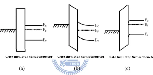
The energy band diagrams and the schematics of TFTs operation in an n-type accumulation mode as shown in Figs. 2-2 and 2-3 are introduced to explain the three operation modes of TFTs. When no gate voltage is applied, the semiconductor is in an equilibrium state. After a negative bias is applied on the gate electrode, the delocalized electrons in the channel are repelled from the semiconductor/gate insulator interface. The effect creates a depletion region of positive charge, as indicated by the positive curvature in the conduction band and the valance band near the insulator as shown in Fig. 2-2 (b). This result conducts the depletion region of carriers as shown in Fig. 2-3 (b). The higher bias on the gate electrode, the larger depletion the region expands. Finally, all of the semiconductor layer will be depleted. When a positive gate bias is applied, delocalized electrons in the channel are attracted to the semiconductor/gate insulator interface, and creating electron accumulation at the interface. The outcome can be indicated by the negative curvature in the conduction band and valance band near the insulator as shown in Fig. 2-2 (c). Then, the accumulation region is formed as shown in Fig. 2-3 (c). These accumulated electrons at the semiconductor/insulator interface provide a current conduction path and form the channel.
15
(a) (b)
Fig. 2-1 Schematic view of (a) top contact and (b) bottom contact TFTs, respectively.
(a) (b) (c)
Fig. 2-2 The semiconductor energy band diagram when (a) unbiased, (b) negative gate voltage bias, and (c) positive gate voltage bias, respectively.
(a) (b) (c)
Fig. 2-3 Schematic of TFTs operation in accumulation mode: (a) unbiased, (b) negative gate voltage bias, and (c) positive gate voltage bias, respectively.
16
2.3 The Method of Parameter Extraction
In this section, the methods of typical parameter extraction such as threshold voltage (Vth), subthreshold swing (S.S.), on/off current ratio (Ion/Ioff) and field effect mobility (μFE) from device characteristics will be introduced.
(1) Mobility
The μFE is defined as the transportation ability of electrons or holes in a conductor or a semiconductor. There are many methods to estimate μFE. In this thesis, the mobility is extracted by the measured results and the transconductance (gm) at low drain bias mentioned in equations 2.3. The TFTs transfer I-V characteristics can be expressed as
2 2 1 D D th G OX FE D V V V V L W C I (2-1) whereCOX is the gate oxide capacitance per unit area W is channel width
L is channel length
Vth is the threshold voltage VG is gate electrode voltage VD is drain electrode voltage
If VD is much smaller than VG – Vth and VG > Vth, the drain current can be approximated as:
G th
D OX FE D V V V L W C I (2-2) The transconductance is defined as:m FE OX VD L W C g (2-3) Thus,
17 m D OX FE g WV C L (2-4) The mobility value is taken from equations 2-4 with maximum μFE.
(2) Threshold Voltage
Vth is defined from the gate to source voltage at which carrier conduction happens in TFTs channel. Vth is related to the gate insulator thickness and the flat band voltage. Plenty of methods are available to determine Vth which is one of the most important parameters of semiconductor devices. This thesis adopts the constant drain current method in which the voltage at a specific drain current NID is taken as Vth, where NID denotes normalized drain current. Constant current method is adopted in most studies of TFTs. It provides a Vth close to that obtained by the complex linear extrapolation method. Generally, the threshold current NID = ID/(W/L) is specified at 1 nA in linear region and at 10 nA in saturation region; L and W denote TFTs channel length and width, respectively [14].
(3) Ion/Ioff
When a device is operated in accumulation mode, the amount of carriers is accumulated in the channel, and the resistance becomes less. This state is called “on state”. When a device is operated in depletion mode, carriers neared the channel are depleted, and this state is called “off state”. The ratio of the largest current to the smallest current is called Ion/Ioff. There are many methods to determine the on and off currents. The practical one is to define the maximum leakage current as off current when drain voltage is applied at 4.5 V. High on/off current ratio represents not only the large turn-on current but also the small off current. The on/off current ratio affects the AMLCD gray levels directly.
18
(4) Subthreshold Swing
S.S. defined as the amount of gate voltage required to increase and decrease drain current by one order of magnitude is a typical parameter to describe the control ability of gate toward channel which is the speed of turning the device on and off. S.S. should be independent of drain voltage and gate voltage. However, in reality, S.S. increases with drain voltage due to short channel effects such as charge sharing, avalanche multiplication and punchthrough-like effect. The subthreshold swing is also related to gate voltage due to undesirable factors such as resistance and interface state. In this thesis, S.S. is defined as one-half of the gate voltage required to decrease the threshold current by two orders of magnitude (from 10-8A to 10-10A). The threshold current is specified to be the drain current when the gate voltage is equal to Vth.
2.4 Origin of Instability in a-IGZO TFTs
2.4.1 The Behavior of a-IGZO TFTs in the Ambience
The carrier concentration of a-IGZO is related to the oxygen vacancy. One oxygen vacancy can provide two electrons in the film. Therefore, the oxygen vacancies are strongly associated with the electrical characteristics of the a-IGZO TFTs. For the a-IGZO film, the absorption of oxygen and moisture can affect the oxygen vacancies in the film. The adsorbed oxygen will fill in the oxygen vacancies and capture electrons as shown in Fig 2-4 (a). This fact can form a depletion layer below the a-IGZO film, hence shifting the Vth positively [19]. However, the adsorbed moisture as shown in Fig 2-4 (b) can act as the electron trapping center as well as electron donors in the a-IGZO film and that the Vth moves in the negative direction [19]. Obviously, the interaction between the backchannel of a-IGZO and the ambience plays a critical role in determining the Vth instability.
19
2.4.2 The Behavior of a-IGZO TFTs under Illumination
The energy band gap of the a-IGZO film is about 3 eV. The result means a change of electrical performance takes place when the wavelength is under 410 nm. When the light with energy larger than 3 eV is absorbed, the electrons can get enough energy to transit from valence band to conduction band and generate a large density of electron-hole pairs that are separated in the device channel. Therefore, the holes are trapped within the channel or/and at the SiO2/a-IGZO interface, as shown in Fig. 2-5 (a), and electrons can be more mobile than hole in a-IGZO film, as shown in Fig. 2-5 (b). This consequence will shift the Vth to more negative values and increase the off-state drain current.
2.4.3 The Mechanism of a-IGZO TFTs in Voltage Stress
The studies of TFTs have results in two proposed mechanisms to explain the electrical instabilities as shown in Fig. 2-6 [28.29]. One is carrier trapping in the gate insulator where the high density of defects can trap charge when the gate electrode undergoes a bias stress. The electrons inject into the gate insulator that can cause the Vth shift. The other is the defect creation in the a-IGZO layer or at the gate insulator/a-IGZO interface that increases the density of deep gap states. When a positive gate bias causes electrons to accumulate at the gate insulator/a-IGZO interface, most of the electrons reside in conductive band tail states that enhance a metastable in the density of deep defect states. The increase in the number of defect states causes the Vth to enlarge.
20
(a) (b)
Fig. 2-4 The schematic diagram showing the role of (a) oxygen as an electron acceptor and (b) water molecules as a electron donor onto a-IGZO surface, respectively. [19]
(a) (b)
Fig. 2-5 (a) Band diagram of a-IGZO TFTs operated under illumination and (b) closer look at the channel region, respectively.
21
Fig. 2-6 Energy band diagram of a-IGZO TFTs (a) electron injection and trapping within the gate insulator, (b) deep state creation and (c) electron trapping within the a-IGZO channel layer, respectively. [28]
2.5 The Mechanism of Gas Permeation
To discriminate the quality of the passivation layer, the mechanism of gas permeation need to be introduced. It can be explained by solution-diffusion model as shown in Fig. 2-7. First, gas adsorption and condensation happen on the surface of the film. Subsequently, the condensed molecules dissolve into the film to some degree and then diffuse down in the film. Finally, the gas molecules desorb out of the film. According to the model, the rate of gas permeation is related to the dissolubility of the surface, the rate of diffusion in the film, the thickness of the film, and the pressure difference in the two side of film.
22
Fig. 2-7 Solution-diffusion model. [30]
2.6 Summary
The a-IGZO shows the unique property such as the film can be deposited at room temperature (RT). Therefore, a-IGZO TFTs can be fabricated at RT by using sputtering system, consequently applicable for flexible TFTs on polyethylene terephthalate (PET) sheets. For practical applications, the stability and reliability of a-IGZO TFTs must be studied by finding out the origin of instability in a-IGZO TFTs and a feasible passivation layer to enhance the stability and reliability of a-IGZO TFTs.
23
Chapter 3
Experiments
3.1 Introduction
The bottom gate structure of a-IGZO TFTs with the SiOx or SiNx films as the passivation layer were used to analyze the features of passivation function. In this chapter, the fabrication flow of a-IGZO TFTs will be described, and the fabrication facilities, materials and the analyzers will be listed. The devices measurement and the passivation layer analyses will be described. The performances of TFTs were measured by a Keithley 4200 analyzer. The surface profile and the film quality were examined by atomic force microscope (AFM) and scanning electron microscope (SEM), respectively.
3.2 Process Design and Schemes
To study the stability and reliability of a-IGZO TFTs devices with passivation, the study can be divided into two parts as shown in Fig. 3-1. One is the passivation film observation. Using atomic force microscope (AFM) and scanning electron microscope (SEM) observe the top view of the SiOx and SiNx films, respectively. Besides, the cross section of the two materials is also examined by SEM. To quantize the ability of the two materials as the passivation, moisture content is measured by Karl Fischer moisture titrator. The transmittance and hydrophobic ability of the two materials is also measured by Ultraviolet-visible spectroscopy and Contact Angle Detector, respectively. Then a comparison of SiOx and SiNx
24
is presented. We then studied the bottom gate a-IGZO TFTs with passivation. The electrical properties of a-IGZO TFTs with the two materials in the ambience and under light illumination are characterized, followed by the discussions of these devices by voltage stress.
Fig. 3-1 Flowchart of the study.
3.3 Materials and Instruments
In this experiment, a large amount of materials and process instruments were used. The arrangement of materials titles and the application of materials in this section are summarized in Table. 3-1. The characterization equipments and fabrication facilities are listed in Tables 3-2 and 3-3, respectively.
25
Table 3-1 Experimental materials
Material Chemical Formula Application
Si wafer Si Substrate
Quartz SiO2 Substrate
IGZO target In:Ga:Zn:O=1:1:1:1 Active layer
SiNx target SiNx Passivation layer
SiOx target SiOx Passivation layer
Aluminum metal Al (99.9%) Electrode
Table 3-2 Measurement instruments
Instruments Company Purpose
Semiconductor Analyzer Keithley 4200 Device performances characterization Atomic Force Microscope Veeco DI 3000 Film morphology and thickness
observation
UV-visible Spectroscopy Lambda 950 The transmittance of passivation layer measurement
Karl Fischer Moisture Titrator KEM MKS 520 Moisture content measurement Contact Angle Detector Paul. N. Gardner Hydrophobic ability of passivation
layer observation
Scanning Electron Microscope Hitachi S-4700I Cross section of passivation layer observation
26
Table 3-3 Fabrication instruments
Instruments Company Function
Wet Bench SYNREX Si wafer clean
Sputtering machine Kaoduen Active and passivation layer deposition Thermal Evaporator ULVAC Electrodes deposition
3.4 The Fabrication Process of a-IGZO TFTs
In this experiment, a bottom gate structure was selected. A heavy doped (N++) n type Si wafer with 100 nm thermal oxide layer was used as the gate electrode and insulator, respectively. The active layer and passivation layer were deposited by sputtering process. The source/drain electrodes were deposited by thermal evaporation. The details of each fabrication process, as shown in Fig. 3-2, are described in the following section.
(1) Substrate Cleaning
The dimensions of substrate (Si) are 3 cm x 3 cm. The substrates were cleaned by DI water for 5 minutes and HF solution (HF: H2O=1: 100) for 10 seconds, respectively. Sequentially, the cleaning was done by blowing off the moisture with N2 jet and baking at 100°C for 1 hour.
(2) Active Layer Deposition
The sputter system as shown in Fig. 3-3 with a background pressure < 4 × 10⁻⁶ torr was employed to deposit a-IGZO thin films. A 40 nm thick a-IGZO (In: Ga: Zn: O =1: 1: 1: 1) active layer as shown in Fig. 3-2 (b) was deposited in a high vacuum system where the
27
target-to-target distance is 10 cm. The deposition was done at RF power = 80 W without any intentional substrate heating, working pressures 3m torr, oxygen and argon flow rate were equal to 0.6 sccm and 10 sccm, respectively.
(3) Metal Electrodes Deposition
The thermal evaporation system, as shown in Fig. 3-4, with a background pressure at about 3 x 10⁻⁶ torr was employed to deposit aluminum (Al) electrodes. The 50 nm thick Al source/drain electrodes, as shown in Fig. 3-2 (c), were deposited through a shadow mask. The evaporation rate of Al was set about 1 Å /sec at a pressure of 5 x 10⁻⁶ torr.
(4) Passivation Layer Deposition
The sputter system, as shown in Fig. 3-3, with a background pressure < 4 × 10⁻⁶ torr was employed to deposit a-IGZO thin films. A 50 nm thick passivation layer as shown in Fig. 3-2 (d) was deposited in a high vacuum system where the target-to-target distance is 10 cm. The deposition was done with RF power for SiOx and SiNx in 100W and 90W, respectively without any intentional substrate heating, working pressures 3m torr, and argon flow rate was equal to 10 sccm.
(5) Annealing Process
Finally, the device was thermally annealed in nitrogen ambience at 350℃ for 1 hour by atmospheric anneal furnace to rearrange the a-IGZO and the passivation lattice again. Fig. 3-5 shows the instrument of atmospheric anneal furnace. The fabricated devices are shown in Fig. 3-6.
28
29
Fig. 3-3 Sputter system in NCTU.
30
Fig. 3-5 Tube furnace in NCTU.
31
3.5 The Principle of Sputtering
The sputtering system can be classified into two types: RF and DC due to the power supply system. RF sputtering can be applied to sputter both insulating and conductive targets. However, DC sputtering can only be used to sputter conductive targets. The flux of electrons from the DC supply causes charges to build-up on the surface of an insulating target, rendering the plasma unstable so that it eventually extinguishes. In the thesis, a RF sputtering system is used as shown in Fig. 3-7. A RF power operates at 13.56 MHz to generate plasma. The plasma creates ions which can be accelerated toward the target by a negative DC bias on the target. The ions can dislodge the target atoms and then deposit onto the substrate. The sputtering system is operated in vacuum, typically between 1 mTorr and 50 mTorr. A lower chamber pressure increases the mean free path which results in the deposited species to have more energy to diffuse along the substrate surface to find the lowest energy state possibility.
32
3.6 Devices Measurement and Analysis
(1) Top View and Cross Section of Passivation Layer
The atomic force microscope (AFM) was utilized to measure the passivation layer morphology at room temperature and atmosphere. The operation of AFM was set to tapping mode which can prevent the probe from damaging the sample surface and can get more precise surface topographic information and the probe oscillation frequency was 300Hz. A laser beam reflected by the cantilever detects the tiny vibration of the cantilever, as shown in Fig. 3-8. The feedback amplitude and the phase signals of the cantilever were recorded by the computer and provided the morphology information.
The scanning electron microscope (SEM) was used to measure the passivation layer morphology and cross section in vacuum. In a typical SEM as shown in Fig. 3-9, an electron beam is emitted from an electron gun fitted with a tungsten filament cathode and is focused by one or two condenser lenses to a spot about 0.4 nm to 5 nm in diameter. The energy exchanged between the electron beam and the sample results in the reflection of electrons by elastic scattering, emission of secondary electrons by inelastic scattering and the emission of electromagnetic radiation. The resulting image is a distribution map of the intensity of the signal being emitted from the scanned area of the specimen. Before the measurement, the samples must be coated with a conductive layer to release the electrons when the electron gun hits to the samples.
33
Fig. 3-8 A schematic model of AFM.
34
(2) Affinity of Passivation Layer Observation
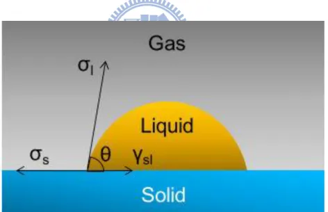
Affinity of passivation layer materials was measured by the contact angle detector. The concept of static measurement mode is illustrated in Fig. 3-10 with a small liquid droplet resting on a flat horizontal solid surface. The symbols σs and σl denote the surface tension components of the two phases. The symbol γsl represents the interfacial tension between the two phases, and θ denotes the contact angle corresponding to the angle between vectors σl and γsl. The relationship between these parameters is the Young’s equation (σs = γsl + σl×cosθ). The contact angle is specific for any given system and is determined by the interactions across the gas-solid-liquid interfaces. The measurement was used to estimate wetting properties of a localized region on a solid phase. The DI water droplets were employed as the reference and the contact angle of passivation layer was measured directly without surface pretreatment.
Fig. 3-10 The contact angle formation of liquid on solid surface.
(3) Measurement of Moisture Content
The moisture content of SiOx and SiNx as passivation were measured by Karl Fischer moisture titrator, as shown in Fig. 3-11, where moisture in sample reacts with Karl Fischer reagent quantitatively based on the following formula: I2 + SO2 + 3 Base + ROH + H2O → 2
35
Base‧HI + Base‧HSO4R. Base denotes amine and pyridine, etc. ROH represents 2-methoxyethanol and methanol, etc. According to a known factor of Karl Fischer reagent, the moisture concentration of the unknown sample can be calculated. Before the moisture content measurement, three different samples included the substrates without passivation, with SiOx as passivation and with SiNx as passivation were prepared. The samples were put into 60℃ and 95% relative humidity condition for five days.
Fig. 3-11 The construction of Karl Fischer moisture titrator.
(4) Measurement of Transmittance in Passivation Layer
The transmittance of SiOx and SiNx as passivation deposited on quartz substrate were measured by Ultraviolet-visible spectroscopy, as shown in Fig. 3-12. The basic parts of a spectroscopy are a light source, a holder for the sample, a diffraction grating or monochromator to separate the different wavelengths of light, and a detector. The intensity of
36
light before it passes through the sample (Io) compares to the intensity of light passing through a sample (I). The ratio I/Io is called the transmittance, and is usually expressed as a percentage (%T). Quartz substrates were used to minimize the back ground interference during transmittance measurement. The transmittance of the samples was scanned from 200 nm to 800nm.
Fig. 3-12 A schematic of Ultraviolet-visible spectroscopy.
(5) Measurement of Electrical Characteristics of a-IGZO TFTs
The transfer characteristics and output characteristics were carried out by Keithley 4200 analyzer. The gate voltage was sweep from -10V to 40V in transfer characteristic measurement. The device parameters including threshold voltage (Vth), field effect mobility (μFE) and subthreshold swing (S.S.) were also extracted. In output characteristic measurement, the drain voltage was sweep from 0 V to 40 V.
In voltage stress, the drain and gate voltage were set at 20V and the stress time is 5000 sec. Every 500 sec, the transfer characteristics were measured.
37
filters and an optical fiber was used. The monochromic light passed through a fiber cable and probe station microscope used to focus the light illumination on the specific devices.
3.7 Summary
The bottom gate a-IGZO TFTs with passivation were fabricated. The properties of passivation layer were examined by AFM, SEM, contact angle detector, Karl Fischer moisture titrator and Ultraviolet-visible spectroscopy, respectively. The stability and reliability of a-IGZO TFTs were studied after deposited a passivation layer. The electrical properties of those devices were measured by a Keithley 4200 analyzer. All of the experimental results and discussions will be given in Chapter 4.
38
Chapter 4
Results and Discussion
4.1 Introduction
The bottom gate a-IGZO TFTs with/without passivation were fabricated to characterize the stability and reliability. The physical properties of the SiOx and SiNx films as the passivation layer such as density, affinity, and transmittance will be presented. The electrical characterizations of a-IGZO TFTs with/without passivation in the ambience, under light illumination, and in voltage stress will also be discussed.
4.2 Analysis of the Passivation Layer
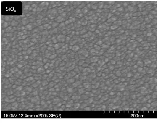
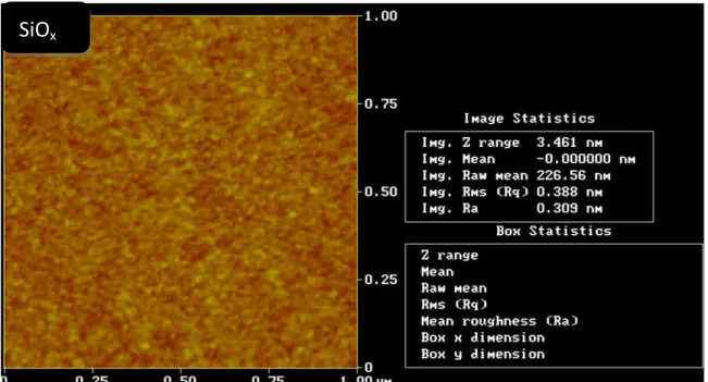
4.2.1 Film Morphology Analysis
The high density is a basic property for material as passivation. A growth of film can be divided into three steps, as shown in Fig. 4-1. First, the resolution limit step, the resolution of film growth depends on the interaction between film molecules and surface molecules of substrate. Second, the diffusion limit aggregation step, where molecules diffuse on a surface and stick to any existing island without further diffusion. Third, the coarsening step, the film islands coarsen until the grains touch each other. The top view images of the SiOx and SiNx film are characterized by SEM, as shown in Fig. 4-2. Both of the two films are confirmed to complete the three steps of the deposition films. The morphology of the SiOx and SiNx film is also observed by AFM, as shown in Fig. 4-3. The surfaces roughness of the SiOx and SiNx
39
film is of less than 1 nm. The flat passivation films are suitable for following top electrode process to assemble a back plane of the TFT-LCD.
(a) (b) (c)
Fig. 4-1 Growth steps of film: (a) the nucleation, (b) the diffusion, and (c) the coarsening step, respectively. [31]
40
(a) SiOx
(b) SiNx
Fig. 4-2 SEM image of (a) the SiOx film and (b) the SiNx film deposited by sputtering, respectively.
SiO
x41
(a) SiOx
(b) SiNx
Fig. 4-3 AFM morphology of (a) the SiOx film and (b) the SiNx film deposited by sputtering, respectively.
SiN
x42
4.2.2 Cross-section Observation
According to the mechanism of gas permeation, the rate of gas permeation is related to the dissolubility of the surface, the rate of diffusion in the film, the thickness of the film, and the pressure difference in the two sides of film. In this experiment, the thickness of the film and the pressure difference in the two sides of film are the same. The rate of diffusion in the film is related to the density of the material. The SEM photos of the cross section of the SiOx and SiNx film, as shown in Fig. 4-4, can be directly used to investigate the density of the film. Compared with the cross section photos of the SiOx and SiNx film with the same thickness, the SiOx film clearly has more cavities. The result indicates the SiOx film has lower density than the SiNx film. Therefore, the SiNx film has a better structure as passivation to isolate the a-IGZO film from oxygen and moisture in the ambience.
43
(a) SiOx
(b) SiNx
Fig. 4-4 The cross section image of (a) the SiOx film and (b) the SiNx film deposited by sputtering, respectively.
44
4.2.3 Moisture Content
With the cross section photo of the SiOx and SiNx films, the SiNx films has fewer cavities to be a more suitable passivation layer. To quantize the density of the SiOx and SiNx films, the moisture content of the three different samples were measured. The three samples are the a-IGZO film on the substrate, the a-IGZO film with SiOx as passivation, and the a-IGZO film with SiNx as passivation, respectively. The moisture content in the three samples, as shown in Fig.4-5, shows that the a-IGZO film easy to absorb moisture and increase the interaction with moisture. Nevertheless, the a-IGZO film with the SiOx or SiNx film as passivation can reduce the moisture content. The a-IGZO film with SiNx has the lowest value of moisture content, confirmed that the SiNx film has a higher density in structure to prevent the a-IGZO film from interacting with oxygen and moisture in the ambience.
IGZO SiOx / IGZO SiNx / IGZO 0 800 1600
m
o
is
tu
re
c
o
n
te
n
t
(p
p
m
)
film
Fig. 4-5 The moisture content of the three samples included the a-IGZO film, the a-IGZO film with SiOx as passivation, and the a-IGZO film with SiNx as passivation measured by Karl Fischer moisture titrator, respectively.
45
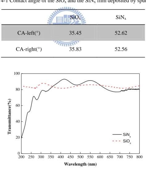
4.2.4 Contact Angle Measurement
The dissolubility of the surface and the rate of diffusion in the film are the important issues for materials as passivation. The rate of diffusion in the film was studied by the cross section microphotograph and moisture content, respectively. The contact angle measurement reveals that the hydrophobic ability of the SiOx and SiNx films is related to the dissolubility of the surface. The hydrophobic property of the material can decrease the rate of dissolubility on the interface. The photographs of de-ion water (DI water) drop on the SiOx and SiNx films are shown in Fig. 4-6, respectively. The contact angle of the SiOx and SiNx films is summarized in Table 4-1. The sequence of contact angle is SiNx > SiOx. The higher contact angle indicates a more hydrophobic property and signifies a lower dissolubility occur on the surface. As a result, the SiNx films are a more suitable to reduce the rate of gas permeation.
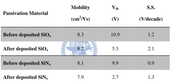
4.2.5 Transmittance
The optical energy band gap of the a-IGZO is about 3 eV that may cause the electrical instability for a-IGZO TFTs under near-ultraviolet illumination. Consequently, precaution is necessary to block the a-IGZO film from interacting with the photo energy over 3 eV. The transmittance of the SiOx and SiNx film were measured by ultraviolet-visible spectroscopy, as shown in Fig. 4-7. The SiOx film can almost be transmitted from 200 nm to 800 nm. Nevertheless, the SiNx film has low transmittance under 80 % when the wavelength is lower than 350 nm. According to the definition of transmittance (T) and absorbance (A):
T
Alog10 , low transmittance represents high absorbance. Accordingly, the SiNx film can
prevent the back channel of a-IGZO from light illumination when the wavelength is under 350 nm.
46
(a) (b)
Fig. 4-6 Contact angle for DI water drop on the (a) SiOx and (b) SiNx film deposited by sputtering, respectively.
Table 4-1 Contact angle of the SiOx and the SiNx film deposited by sputtering
SiOx SiNx CA-left(°) 35.45 52.62 CA-right(°) 35.83 52.56 200 250 300 350 400 450 500 550 600 650 700 750 800 0 20 40 60 80 100 T r a n sm it ta n c e (% ) Wavelength (nm) SiN x SiO x
47
4.3 Electrical Characteristics Analyses of Passivated a-IGZO TFTs
The results of material properties lead the conclusion that, the SiOx and SiNx films can be used as passivation layer. The important issue is the electrical properties of the devices after the deposition of the passivation layer on the back channel of a-IGZO TFTs. Therefore, the comparison of electrical characteristics before and after deposited a passivation layer is carried out.
4.3.1 The a-IGZO TFTs Before and After Deposited SiO
xas Passivation
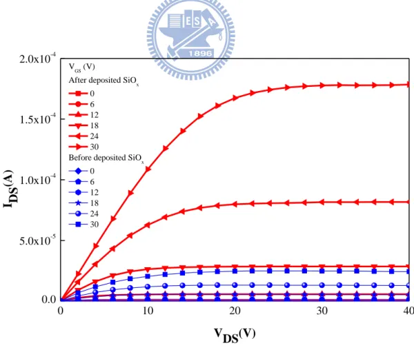
The transfer characteristics of a-IGZO TFTs before and after deposited SiOx are illustrated in Fig. 4-8, and some parameters are summarized in Table 4-2. The initial electrical performances are 8.3 cm2/Vs of μFE, 1.2 V/decade of S.S., and 10.9 V of Vth. After the deposition of SiOx, the same device exhibits 8.2 cm2/Vs of μFE, 2.1 V/decade of S.S., and 5.3 V of Vth. The saturation drain current of passivated a-IGZO TFTs increases by about 12 % compared to that of the a-IGZO TFTs before deposited the passivation layer. Fig. 4-9 presents the output characteristics of a-IGZO TFTs before and after deposited SiOx. The ID-VD figures have no current crowding effect at low VDS values, indicating there is no significant series resistance to the source-drain.
4.3.2 The a-IGZO TFTs Before and After Deposited SiN
xas Passivation
The transfer characteristics of a-IGZO TFTs before and after deposited SiNx are shown in Fig. 4-10, and some parameters are summarized in Table 4-2. The initial electrical performances are 8.1 cm2/Vs of μFE, 0.9 V/decade of S.S., and 9.9 V of Vth. After the deposition of SiNx, the same device possesses 7.9 cm2/Vs of μFE, 1.3 V/decade of S.S., and
48
2.7 V of Vth. The saturation drain current of passivated a-IGZO TFTs increases by about 53 % compared to that of the a-IGZO TFTs before deposited the passivation layer. Fig. 4-11 shows the output characteristics of a-IGZO TFTs before and after deposited SiNx as passivation. The ID-VD figures have no current crowding effect at low VDS values, indicating there is no significant series resistance to the source-drain.
Table 4-2 Comparison of device performances before/after deposited SiOx and SiNx as passivation Passivation Material Mobility (cm2/Vs) Vth (V) S.S. (V/decade) Before deposited SiOx 8.3 10.9 1.2
After deposited SiOx 8.2 5.3 2.1
Before deposited SiNx 8.1 9.9 0.9
After deposited SiNx 7.9 2.7 1.3
4.3.3 Discussion
The difference in the electrical characteristics of the a-IGZO TFTs before and after deposited a passivation layer is attributed to the deposition process and the interface of the a-IGZO and the passivation layer. The ion bombardment at sputtering can break the metal-oxygen bonding that creates the oxygen vacancy on the back channel surface and generates free carriers in the a-IGZO film. For metal oxide, the carrier concentration is related to the oxygen vacancy. The less oxygen vacancies in the a-IGZO film lead a higher voltage to turn on the channel. Consequently, this ion bombardment effect generates more oxygen
49
vacancies to enhance the a-IGZO film conductivityand lower the Vth. The effect of passivated TFTs, as shown in Fig. 4-12, has been studied [34]. The surface band bending, EC-EqF, and the current density, Jx, explain that the passivated TFTs have more positive fixed charge at the back interface. Some free electrons are accumulated in the back interface which is controlled by the gate bias. The band bending provides a conductive path for electrons at a-IGZO/passivation layer interface. More negative gate bias is required to turn off the TFT by depleting the carriers at the back-channel. Thus, the Vth has a negative shift after the deposition of the passivation layer.
The leakage current of SiOx and SiNx as passivation affects the electrical properties of a-IGZO TFTs. We used a Metal-Insulator-Metal (MIM) structure device to measure the leakage current of SiOx and SiNx by a Keithley 4200 semiconductors parameter analyzer. The results show 9×10⁻⁶ A/cm2 and 3×10⁻⁶ A/cm2 for SiOx and SiNx in 1 MV/cm, respectively. Therefore, the leakage current has to be depleted to turn off the TFT at operation by more negative gate bias.
The increase of the conductivity of the a-IGZO film caused by the ion bombardment and the back channel current induced by positive fixed charge at the back interface explain the raise of the drain current. According to the formula of the TFTs transfer I-V characteristics, the drain current can be approximated as:
.2 2 th G OX FE D V V L W C I The parameters of W,
L and Cox are constant in the same device. As a result, the decrease in the Vth also can account for the raise of the drain current as the data reveal.
![Fig. 1-5 Transmittance of a-IGZO in visible light. [14]](https://thumb-ap.123doks.com/thumbv2/9libinfo/8222825.170618/19.892.219.742.257.687/fig-transmittance-igzo-visible-light.webp)
![Fig. 1-6 The display image of Samsung’s 12.1 inch WXGA AMOLED display. [15]](https://thumb-ap.123doks.com/thumbv2/9libinfo/8222825.170618/20.892.237.704.111.420/fig-display-image-samsung-inch-wxga-amoled-display.webp)