國 立 交 通 大 學
電信工程學系
碩 士 論 文
可設定式雙模低失真類比數位轉換器
Configurable Dual-mode Low-distortion
A/D Converter
研究生:林明澤
指導教授:洪崇智 博士
可設定式雙模低失真類比數位轉換器
Configurable Dual-mode Low-distortion A/D Converter
研 究 生:林明澤 Student:Ming-Tze Lin
指導教授:洪崇智 博士 Advisor:Dr. Chung-Chih Hung
國 立 交 通 大 學
電 信 工 程 學 系 碩 士 班
碩 士 論 文
A Thesis
Submitted to Department of Communication Engineering College of Electrical Engineering and Computer Science
National Chiao Tung University In Partial Fulfillment of the Requirements
For the Degree of Master In
Communication Engineering October 2007
Hsinchu, Taiwan.
可設定式雙模低失真類比數位轉換器
研究生:林明澤 指導教授:洪崇智 教授
國立交通大學
電信工程學系碩士班
摘要
隨著多功能裝置需求的快速成長,如手機、mp3 播放器等,多功能在今日已 經變得越來越重要。在今日的裝置應用,數位電路主導整個晶片的面積。無論如 何,類比轉數位介面是不可少的。使用超取樣與雜訊型化的三角積分器調變器是 非常有效的技術應用在高解析度類比數位轉換器上。它本身對原件不匹配與漂移 非常不敏感,而這項特點非常適合今日的 VLSI 設計。考慮兩種三角積分調變器, 應用在音頻的三角積分調變器與應用在量測的累加調變器, 他們擁有相似的架 構,並且可以用共用或者整合的方式設計在一起。因此,這個可調式超取樣類比 數位轉換器不僅可以擁有兩種功能,並且可以減少晶片面積。除此之外,多級或 疊接調變器,也叫做 MASH,在實現方面不會有穩定性的問題還可以更適合做設 計上的控制。此外,向前饋入的架構更適合此種電路,讓它有低失真的效果。 因此,為了將兩種電路合併用低失真 MASH 的架構實現,這個研究重點放在 如何設計可設定式雙模低失真類比數位轉換器。晶片是以台積電 0.18 微米標準 互補式金氧半導體製程所製造。在音頻應用上使用過取樣率 128,也就是操作頻 率為 5.12 MHz,量測結果是 58 dB 動態輸入範圍和 55 dB 訊號失真雜訊比。在 量測應用上使用操作頻率 5.12 MHz 的量測結果與預測使用同樣的轉換時間相比 低 3 bit。這個論文證明此架構引導出一種簡單且模組化的架構。Configurable Dual-mode Low-distortion A/D Converter
Student:Ming-Tze Lin Advisor:Prof. Chung-Chih Hung
Department of Communication Engineering
National Chiao Tung University Hsinchu, Taiwan
Abstract
With the rapid growth in demand for multi-function device such as cellular phone and MP3 player, multi-function has become more and more important today. In today’s device application, digital circuits dominate the whole chip function. However, the analog-to-digital converter (ADC) is indispensable. The Sigma-delta modulation, associated with oversampling and noise shaping, is a well-known technique used in high-accuracy A/D converters. It is almost insensitive to component matching and variation and is suitable for today’s VLSI design. Concerning the two sigma-delta modulators, the Sigma-delta modulator for audio application and incremental modulator for measurement, they have similar architectures and can be combined together by sharing or merging their similar parts. Therefore, this configurable oversampling A/D converter can not only have two functions but also reduce the chip area. Besides, multistage or cascade modulators, also called MASH, can be realized without stability problems and more programmable. In addition, feedforward configuration is suitable for this circuit to have low-distortion.
In order to combine the two circuits using feedforward MASH configuration, this research will focus on how to design a configurable dual-mode low-distortion A/D converter. The chip has been fabricated by TSMC 0.18-um CMOS process. With an oversampling ratio of 128 and a clock frequency of 5.12 MHz, the modulator achieves a 58 dB dynamic range and a peak SNDR of 55 dB for audio application. The measured resolution of the measurement application is 3 bit lower than the prediction in the same conversion time with a clock frequency of 5.12 MHz. This thesis
誌謝
隨著這份碩士論文的完成,兩年來在交大的求學生活也即將告一個段落,往 後迎接著我的,又是另一段嶄新的人生旅程。本論文得以順利完成,首先,要感 謝我的指導教授洪崇智老師在我兩年的研究生活中,對我的指導與照顧,並且在 研究主題上給予我寬廣的發展空間。而類比積體電路實驗室所提供完備的軟硬體 資源,讓我在短短兩年碩士班研究中,學習到如何開始設計類比積體電路,乃至 於量測電路,甚至單獨面對及思考問題的所在。此外要感謝李育民教授、黃淑娟 教授、陳科宏教授撥冗擔任我的口試委員並提供寶貴意見,使得本論文更為完 整。也感謝國家晶片系統設計中心提供先進的半導體製程,讓我有機會將所設計 的電路加以實現並完成驗證。 另一方面,要感謝所有類比積體電路實驗室的成員兩年來的互相照顧與扶 持。首先,感謝博士班的學長羅天佑、薛文弘、廖介偉、黃哲揚以及已畢業的碩 士班學長何俊達、黃琳家、蔡宗諺、林政翰、楊家泰和陳家敏在研究上所給予我 的幫助與鼓勵,尤其是俊達學長,由於他平時不吝惜的賜教與量測晶片時給予的 幫助,使得我的論文研究得以順利完成。另外我要感謝白逸維、廖德文、高正昇、 邱建豪、吳國璽、黃旭佑和傅崇賢等諸位同窗,透過平日與你們的切磋討論,使 我不論在課業上,或研究上都得到了不少收穫。尤其是電資718實驗室的同學們, 兩年來陪我ㄧ塊兒努力奮鬥,一起渡過同甘苦的日子,也因為你們,讓我的碩士 班生活更加多采多姿,增添許多快樂與充實的回憶。此外也感謝學弟們林永洲、 郭智龍、夏竹緯、楊文霖,秋楓翔,黃介仁的熱情支持,因為你們的加入,讓實 驗室注入一股新的活力與朝氣。 到這邊,特別要致上最深的感謝給我的父母及家人們,謝謝你們從小到大所 給予我的栽培、照顧與鼓勵,讓我得以無後顧之憂地完成學業,朝自己的理想邁 進,衷心感謝你們對我的付出。 最後,所有關心我、愛護我和曾經幫助過我的人,願我在未來的人生能有一 絲的榮耀歸予你們,謝謝你們。 林明澤 于 交通大學工程四館 718 實驗室 2007.10.1Chapter 1 Introduction ...1
1.1 Motivation...1
1.2 Thesis Organization ...2
Chapter 2 An Overview of Sigma-Delta Data Converters...4
2.1 Introduction...4
2.2 Overview of Analog-to-Digital Data Converters ...4
2.2.1 Categories of Analog-to-Digital Data Converters...4
2.2.2 Oversampling Ratio (OSR)...5
2.2.3 Signal to Noise Ratio (SNR)...6
2.2.4 Signal to Noise and Distortion Ratio (SNDR) ...6
2.2.5 Spurious Free Dynamic Range (SFDR)...7
2.2.6 Dynamic Range (DR) ...7
2.2.7 Effective Number of Bits (ENOB)...7
2.2.8 Overload Level (OL)...7
2.3 Sampling Theorem...8
2.4 White Noise...8
2.5 Oversampling Technique ...10
2.6 Noise Shaping Strategy...13
2.6.1 First-Order Sigma-Delta Modulator ...15
2.6.2 Second-Order Sigma-Delta Modulator ...18
2.6.3 Higher-Order Sigma-Delta Modulator...21
2.6.4 Multi-Stage Sigma-Delta Modulator (MASH) (Cascaded) ...23
2.6.5 System Analysis of Sigma-Delta Analog-to-Digital Converters ...25
2.7 Digital Decimation Filter ...27
2.8 Summary ...30
Chapter 3 Basic Concept of Incremental ΔΣ Converters ...31
3.1 Introduction...31
3.2 Theory and application of incremental ΔΣ converter...31
3.3 High-order incremental converters ...34
3.4 Offset and charge injection compensation ...42
3.4.1 Conversion using analog error compensation...42
3.4.2 Conversion using analog error compensation...44
3.5 Summary ...46
Chapter 4 Design of Configurable Dual-mode Low-distortion A/D Converter ...47
4.1 Introduction...47
4.2 System consideration ...47
4.3 Behavior simulation ...56
4.4.1 Operational Amplifier ...64
4.4.2 Comparator ...67
4.4.3 Clock generator ...69
4.4.4 Bootstrapped switches ...70
4.5 Simulation result ...72
4.6 Layout level design ...75
Chapter 5 Test Setup and Experimental Results ...77
5.1 Introduction...77
5.2 Measuring Environment...77
5.2.1 Power Supply Regulators...79
5.2.2 Input Terminal Circuit...80
5.3 Testing Board, and Pin Configuration...81
5.4 Performance Evaluations of Configurable Dual-mode Low-distortion A/D Converter...82
5.5 Summary ...86
List of Figures
Chapter 1
Chapter 2
Figure 2.1 A general quantizer and its linear model ... 9
Figure 2.2 A possible oversampling system without noise shaping... 10
Figure 2.3 The spectral density of y1(n) after quatization ...11
Figure 2.4 The brick-wall response of the filter to remove out of band quantization noise power ... 12
Figure 2.5 The spectral density of y2(n) after filtering... 12
Figure 2.6 (a) A general noise-shaped sigma-delta modulator (b) Linear model of the modulator showing injected quantization noise... 14
Figure 2.7 A simple block diagram of the first-order low-pass sigma-delta modulator ... 15
Figure 2.8 The block diagram for the first-order low-pass sigma-delta modulator... 16
Figure 2.9 A simple block diagram of the second-order noise shaping SDM ... 18
Figure 2.10 Different order noise shaping curves... 21
Figure 2.11 A simple block diagram of the second-order noise shaping SDM... 21
Figure 2.12 A second-order MASH modulator using two first-order modulators ... 23
Figure 2.13 Block diagram of an oversampling A/D converter... 26
Figure 2.14 Signal and spectra in an oversampling ADC ... 26
Figure 2.15 Multi-stage decimation filters: (a) sinc followed by an IIR filter; (b) sinc followed by halfband filters ... 27
Figure 2.16 Realizing Tsinc(z) as a cascade of integrators and differentiators: (a) downsampling performed after all the filtering; (b) a more efficient method where downsampling is done before the differentiators ... 29
Chapter 3 Figure 3.1 The block diagram of the first-order incremental A/D converter ... 32
Figure 3.2 A third-order cascaded-integrator/feed-forward modulator structure... 34
Figure 3.3 The second-order 1-1 MASH incremental A/D converter... 38
Figure 3.4 The analog error compensation method use discrete-time circuit technique ... 43
Chapter 4
Figure 4.1 The basic concept of the the incremental modulator ... 49
Figure 4.2 The first-order low-distortion topology... 50
Figure 4.3 The second-order incremental modulator using mash 1-1 low-distortion topology ... 52
Figure 4.4 The second-order sigma-delta modulator using mash 1-1 low-distortion topology ... 53
Figure 4.5 Merging digital filters of two type circuits... 54
Figure 4.6 The second-order configurable dual-mode low-distortion A/D convertor .. 55
Figure 4.7 The concept of the higher-order configurable dual-mode low-distortion A/D converter... 55
Figure 4.8 The system architecture of the second-order configurable dual-mode low-distortion A/D converter ... 56
Figure 4.9 The signal swing in each joint of the system... 58
Figure 4.10The spectrum of each joint of the system... 58
Figure 4.11 the input dynamic range of the system ... 59
Figure 4.12The overall spectrum of the system... 59
Figure 4.13 The analog circuit of the second-order configurable dual-mode low- distortion A/D converter and its clock phase ... 60
Figure 4.14 Noise analysis for a single-stage amplifier... 63
Figure 4.16 Folded cascode opamp ... 65
Figure 4.17 The frequency response of the opamp ... 67
Figure 4.18 Low-offset regenerator ... 68
Figure 4.19 The logic test of the comparator ... 69
Figure 4.20 The nonoverlapping clock generator ... 70
Figure 4.21 The two nonverlapping clock signals and its two delayed clock ... 70
Figure 4.22 Bootstrapped switches ... 71
Figure 4.23 The gate voltage of the bootstrapped switch and input signal... 72
Figure 4.24 The time domain of the joints of the proposed configurable dual-mode low-distortion A/D converter ... 73
Figure 4.25 The power spectrum of the proposed configurable dual-mode low-distortion A/D converter ... 73
Figure 4.26 The time domain of the joints of the proposed configurable dual-mode low-distortion A/D converter ... 74
Chapter 5
Figure 5.1 Experimental testing setup ... 77
Figure 5.2 Function generator Agilent 33220A ... 78
Figure 5.3 Logic analyzer Agilent 16702B... 79
Figure 5.4 Oscilloscope Agilent S4832D... 79
Figure 5.5 Power supply regulator... 80
Figure 5.6 Input terminal circuit ... 81
Figure 5.7 Photograph of the dual-mode converter DUT board ... 81
Figure 5.8 (a) Pin configuration diagram and (b) Pin assignment ... 82
Figure 5.9 Measurement result (a) the output of the first stage (b) the output of the second stage ... 83
Figure 5.10 Measured output spectrum ... 84
Figure 5.11 Plot of SNDR versus normalized input signal... 84
List of Tables
Table 2.1 Various Kinds of Analog-to-Digital DataConverters ... 5 Table 4.1 Specification of the first amplifier ... 67 Table 4.2 Specification of the configurable dual-mode low-distortion A/D converter. 75 Table 5.1 Summary of measured results of the SDM ... 85
Chapter 1 Introduction
1.1
Motivation
Recently, as the continued scaling of VLSI technology, the digital circuit has more attractive advantages than analog circuit, such as high level resolution, power
consumption reduction, noise robustness and less chip area. Therefore, analog circuit dominates the whole chip area relative to digital circuit. However, in real world,
human only can sense analog signals. Whether how advanced the digital circuit technique become, the interface to convert analog signal and digital signal is
necessary, which called Analog to Digital Converter(ADC) or Digital to Analog Converter(DAC).
Understanding why reduce chip size is important. The yield (number of good
die/total number of die on the wafer) is increased with smaller die size. Another benefit of reducing die size comes from the realization that processing costs per wafer
are relatively constant. Increasing the number of die on a wafer decreases the cost per die. Therefore, reducing chip area is important, and it can be the result of having
better layout of fabricating the chip in a process with smaller device dimensions.
Along with rapid growth of multi-function device in many applications, such as cellular phone, PDA, and mp3 players, system on a chip (SOC) is an important issue
to help devices become smaller and lighter. How integrate these functions and reduce the chip area is what we want to do.
Oversampling techniques based on sigma-delta modulation offer numerous
advantages for realization of high-resolution analog-to-digital (A/D) converters. First, oversampling converters relax the requirements placed on the analog circuitry at the
expense of more complicated digital circuitry. The other advantage is that they simplify the anti-aliasing filter for A/D converters and smoothing filter for D/A
converters. Besides, it has less chip area than Nyquist rate converters. Then, concerning two different applications of the sigma-delta modulator, sigma-delta
modulator for audio and incremental for measurement, can be designed together in a smart manner. In addition, feedforward configuration does not only relax the linearity
of the opamp but also simplify the mash architecture and improve the input dynamic range.
In this thesis, a 3.066mW, 14-bits for audio, 16-bits for measurement, and
5.12MS/s configurable dual-mode low-distortion analog to digital converter with the 1.8V supply voltage has been designed and implemented with the standard TSMC
0.18μm CMOS 1P6M process.
1.2 Thesis Organization
This thesis is organized into seven chapters.
Chapter 1 briefly introduces the motivation of the thesis.
Chapter 2 describes the concepts of oversampling sigma-delta data converters. First, extra bits of resolution can be extracted from oversampling will be introduced.
described mathematically. Finally, the various architectures of sigma-delta modulators
will be compared.
Chapter 3 describes the concepts of incremental converters. First, the basic operation of the incremental modulator will be introduced. Then, higher order
modulator to reduce conversion time will be discussed. Finally, because of high resolution and offset cancellation for instrumentation application, the offset
cancellation technique will be described.
Chapter 4 presents the system level design consideration. The merging method will be discussed first. After building the behavior model, we continue the circuit level
design, including the operation amplifier, comparator, and nonoverlapping clock generator. The circuits and simulation results will be shown in this chapter.
Chapter 5 presents the testing environment, including the instruments and external
circuits on the printed circuit board (PCB). Measured results for the configurable dual-mode low-distortion A/D converter, which is fabricated in a standard TSMC
0.18μm CMOS mixed-signal process, will be plotted and summarized
Chapter 2 An Overview of Sigma-Delta Data
Converters
2.1 Introduction
In this chapter, the overview of various analog-to-digital converters having difference advantages and drawbacks will be discussed first. Then, the sampling
theorem will be introduced and we shall see that how extra bits of resolution can be extracted from oversampling theorem and how it relax anti-aliasing filter. Next,
getting higher resolution through using noise shaping strategy and digital decimation filter will be discussed mathematically.
2.2 Overview of Analog-to-Digital Data Converters
Although today is an ever-increasing digital world, analog-to-digital converter
also play an important role to translate the digital data from our inherently analog world. However, with the ADC, the input is an analog signal with an infinite number
of values, which then has to be quantized into an N-bit digital word. Then, these digital words can be coded and be transmitted into DSP unit or digital systems.
2.2.1 Categories of Analog-to-Digital Data Converters
There are many different structures to realize analog-to-digital converters.
shown in Table 2.1. There is a trade off between speed and resolution and it is difficult
to design ADCs satisfying both demands at the same time. We shall understand this trade off and choose the adaptable structure for difference application.
TABLE 2.1 Various Kinds of Analog-to-Digital Data Converters
Speed Slow Medium Fast
Resolution High Medium Low
Structure Integrating Oversampling Successive approximation Algorithmic Single-bit pipeline Flash Multiple-bit pipeline Folding Interpolating Time-Interleaved
2.2.2 Oversampling Ratio (OSR)
The oversampling ratio (OSR) of a data converter is a ratio of the sampling frequency to Nyquist-rate. b s f f OSR 2 = (2.1)
where f is the sampling frequency and s f is the signal bandwidth. When the OSR b
is equal to 1 ( fs =2fb), it means the data converter is the Nyquist-rate data converter, however, when the OSR is great than 1, it means the data converter is the oversampling data converter. The OSR is the important parameter for oversampling
data converters. We shall see that the increase in dynamic rage is only 3 dB for every double of the sample rate. To obtain much higher dynamic-range improvement as the
sampling rate is increased, noise shaping through the use of feedback can be used [1].
2.2.3 Signal to Noise Ratio (SNR)
The signal-to-noise ratio (SNR) of a data converter is the ratio of the signal power
to the noise power, which measured at the output of the data converter. A more common SNR formula is to assume input is a sinusoidal waveform. Then, the
theoretical value of SNR for Nyquist-rate ADC is given by
6.02 1.76
SNR= ⋅ +N dB (2.2)
But for oversampling ADC with no noise shaping, the theoretical value of SNR is
6.02 1.76 10 log( )
SNR= ⋅ +N + OSR dB (2.3)
We can see that every doubling the sampling rate will acquire additional 3 dB SNR than Nyquist-rate ADC.
2.2.4 Signal to Noise and Distortion Ratio (SNDR)
The signal to noise and distortion ratio (SNDR) of a data converter is the ratio of
the signal power to the power of the noise plus the harmonic distortion components, which measured at the output of the data converter. The maximum SNDR that a
converter can achieve is called the peak signal to noise and distortion ratio. Generally, SNDR is lower than SNR.
2.2.5 Spurious Free Dynamic Range (SFDR)
The spurious free dynamic range (SFDR) is defined as the ratio of rms value of
amplitude of the fundamental signal to the rms value of the largest harmonic distortion component in a specified frequency range. SFDR may be much larger than
SNDR of a data converter.
2.2.6 Dynamic Range (DR)
The useful signal range, or dynamic range (DR), of the A/D converter for
sinusoidal inputs is defined as the ratio of the output power at the frequency of the input sinusoid for a full-scale input to the output signal power for a small input for
which the SNDR is unity [2].
2.2.7 Effective Number of Bits (ENOB)
For data converter, a specification often used in place of the SNR or SNDR is ENOB, which is a global indication of how many bits would be required to get the
same performance as the converter. ENOB can be defined as follows:
1.76 6.02
SNDR
ENOB= − bits. (2.4)
2.2.8 Overload Level (OL)
OL is defined as the relative input amplitude where the SNR is decreased by 6dB compared to peak SNR value.
2.3 Sampling Theorem
Sampling is the first step for A/D conversion process that transform an analog
input signal into a sequence of digital code. The Nyquist Criterion defines how fast the sampling rate needs to be to represent an analog signal accurately. This criterion
requires that the sampling rate is at least two times the highest frequency contained in the analog signal.
2
s b
f ≥ f (2.5)
We shall know if there is some signal that we don’t want above the highest
frequency, the aliasing will occur. Thus, we shall add a low-pass filter before sampling to filter out the signal above the highest frequency. This low-pass filter, sometimes
called the anti-aliasing filter, must have flat response over the frequency band of interest (base-band) and attenuate the frequencies above the Nyquist frequency
enough to put them under the noise floor, but a low-pass filter having narrow transition band is expensive. We have another way to deal with this problem.
Increasing sampling rate higher than Nyquist frequency will relax the transition band of the anti-aliasing filter. Oversampling converters require considerably simpler
anti-aliasing filters than Nyquist rate converters with similar performance.
2.4 White Noise
We can model a quantizer as adding quantization error e(n), as shown in Figure 2.1. The output signal, y(n), is equal to the closest quantization level value of x(n).
This quantization error is on the order of one least-significant-bit (LSB) in amplitude,
which equals the difference between two adjacent quantization levels.
Figure 2.1 A general quantizer and its linear model
Many of the original results and insights into the behavior of quantization error are
due to Bennett [3]. Bennett first developed conditions under which quantization noise could be reasonably modeled as additive white noise. A common statement of the
approximation is that the quantization error has the following properties, which we call it the “input-independent additive white-noise approximation” [4]:
Property 1. q[n] is statistically independent of the input signal
Property 2. q[n] is uniformly distributed in [-Δ/2, Δ/2], where Δ equals one LSB Property 3. q[n] is an independent identically distributed sequence or q[n] has a flat
power spectral density (white).
Therefore, quantization noise, e(n) can be approximated as an independent random number uniformly distributed between ±∆/2. Thus, the quantization noise power equals Δ2/12 and is independent of the sampling frequency, f . Also, the s
power is within ± fs/2 (a two-side definition of power).
2.5 Oversampling Technique
Oversampling means that the converters operate much faster than the input
signal’s Nyquist-rate. Oversampling can not only relax the requirement of the anti-aliasing filter, but also improve the resolution of the A/D converters. We have
shown how oversampling can relax the requirement of the anti-aliasing filter in section 2.3. Next, we will show how it can increase the output’s signal-to-noise ratio
(SNR) by filtering out quantization noise that is not in the signal’s bandwidth. First, we define the oversampling ratio (OSR) as
b s f f OSR 2 = (2.6)
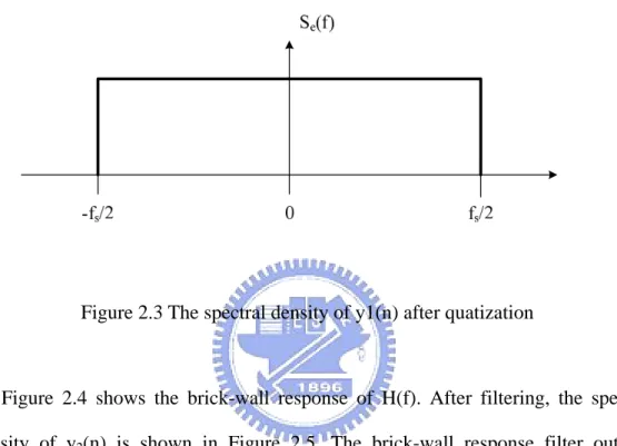
Figure 2.2 shows a possible oversampling system without noise shaping, where
y1(n) is equal to the closest quantized value of input signal, u(n), y1(n) is filtered by H(f) to create the y2(n), and q(n) is the quantization noise.
Assuming the input signal is a sinusoidal wave and quantization noise is white
noise. After quantization, the spectral density of y1(n) is shown in Figure 2.3. We can see that the signal of interest are below ± fb. Since the quantization noise is white noise, it means that noise power is uniformly distributed between − fs/2 and
2 /
s
f
+ .
Figure 2.3 The spectral density of y1(n) after quatization
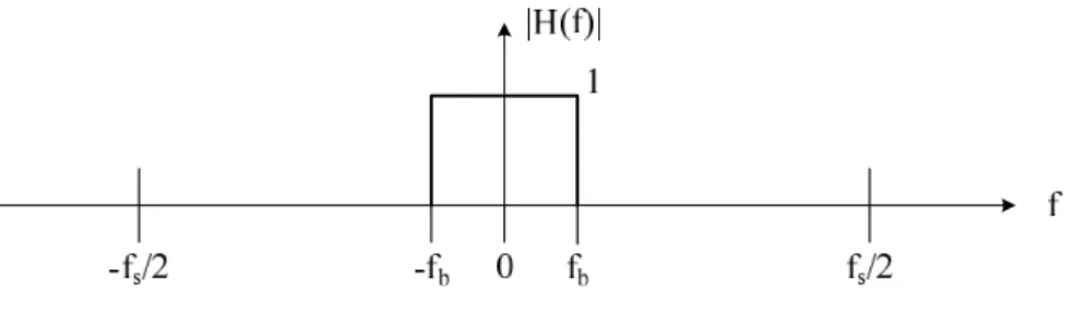
Figure 2.4 shows the brick-wall response of H(f). After filtering, the spectral
density of y2(n) is shown in Figure 2.5. The brick-wall response filter out the quantization noise which are out of our interest bandwidth, and only a small fraction of quantization noise fall into the range of −fb and f . However, we know the b
total power amount of quantization noise is ∆2 12, and the in-band noise power can reduce to ∆ = ∆ × = OSR f fs P b inband e 1 12 12 2 2 2 , (2.7)
Therefore, doubling OSR decrease the quantization noise power by one-half or,
Figure 2.4 The brick-wall response of the filter to remove out of band quantization noise power
Figure 2.5 The spectral density of y2(n) after filtering
Assuming the peak amplitude of the sinusoidal wave is 2N(∆/2)
. For this maximum peak value, the signal power, P , has a power equal to S
8 2 2 2 2N 2 2 2N S P = ∆ ∆ = (2.8)
Now we can calculate the maximum SNR (in dB) to be the ratio of the maximum sinusoidal power to the quantization noise in the signal y2(n). Using (2.7) and (2.8),
the SNRmax is equal to ) log( 10 2 2 3 log 10 log 10 2 max OSR P P SNR N e s + = = (2.9)
which is also equal to
) log( 10 76 . 1 02 . 6 max N OSR SNR = + + (2.10)
N means that N-bit quantizer using in converter, and increasing 1 more bit can improve 6.02 dB SNR. Here, we see that doubling OSR will give SNR 3 dB or,
equivalently, 0.5 bits improvement. The reason for this improvement is the constant quantization noise power uniformly distribute between − fs/2 and + fs/2 . Therefore, after filtering out of band signal power, it remains a little amount of the quantization noise power, and SNR improve.
2.6 Noise Shaping Strategy
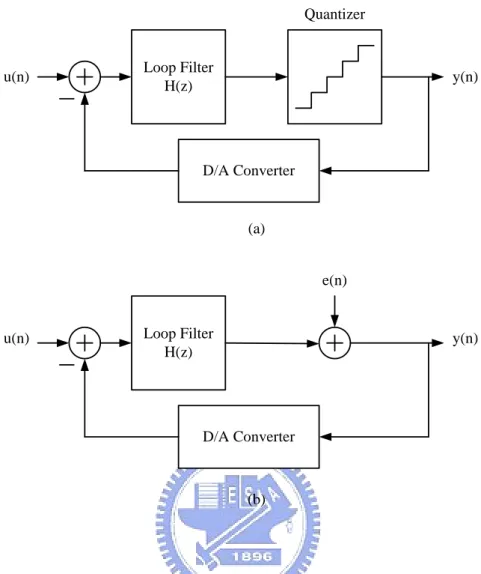
In this section, using feedback to get the advantage of noise shaping the
quantization noise will be discussed. First, a general noise-shaped sigma-delta modulator and its linear model have been shown in Figure 2.6.
Loop Filter H(z) D/A Converter Quantizer y(n) u(n) Loop Filter H(z) D/A Converter y(n) u(n) (a) (b) e(n)
Figure 2.6 (a) A general noise-shaped sigma-delta modulator (b) Linear model of the modulator showing injected quantization noise
Treating the linear model shown in Figure 2.6 as having two independent inputs, u(n) and e(n), we can derive a signal transfer function, STF(z), and a noise transfer function, NTF(z). ) ( 1 ) ( ) ( ) ( ) ( z H z H z U z Y z STF + = ≡ (2.11) ) ( 1 1 ) ( ) ( ) ( z H z E z Y z NTF + = ≡ (2.12)
will be equal to the poles of H(z). In other words, we can control the zeros of the
noise transfer function by choosing the function of the loop filter. We can also using super position to combine two signals, and find out the output as
) ( ) ( ) ( ) ( ) (z STF zU z NTF z E z Y = + (2.13)
The STF generally have all-pass or low-pass frequency response and the NTF
have high-pass frequency response. In other words, the STF will be approximately unity over the signal band and the NTF will be approximately zero over the same
frequency band. The quantization noise will be removed to high frequency band when using noise-shaping strategy [01]. The quantization noise over the frequency
band of interest will be reduced and do not affect the input signal. This would improve the SNR significantly for overall system.
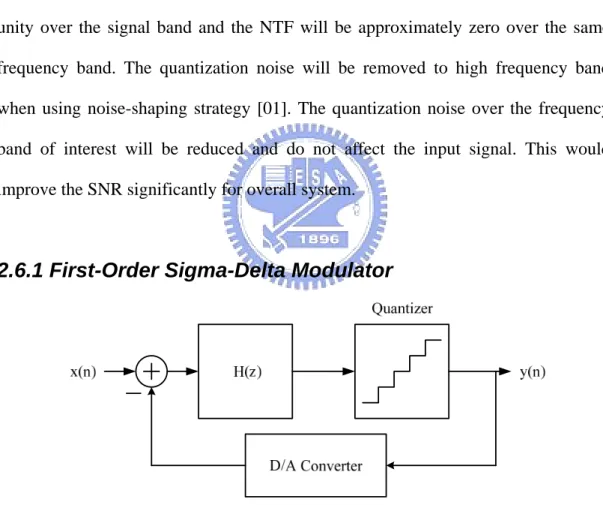
2.6.1 First-Order Sigma-Delta Modulator
Figure 2.7 A simple block diagram of the first-order low-pass sigma-delta modulator
In Figure 2.7, it is a simple block diagram of the first-order low-pass sigma-delta modulator. It includes an integrator and a quantizer. The input of the integrator is the
input signal minus the output signal of the modulator through the DAC. In this
example, since the loop filter is a high-pass filter, the noise function should have a zero at dc (i.e., z = 1). The transfer function of the discrete-time integrator (i.e., have
a pole at z = 1) is 1 1 ) ( − = z z H (2.14)
Its block diagram for such a choice is shown in Figure 2.8.
Figure 2.8 The block diagram for the first-order low-pass sigma-delta modulator
According to (2.11) and (2.12), we can obtain the signal transfer function, ) (z STF , is given by 1 ) 1 /( 1 1 ) 1 /( 1 ) ( ) ( ) ( = − − + − = = z z z z U z Y z STF (2.15)
and the noise transfer function, NTF(z), is given by
) 1 ( ) 1 /( 1 1 1 ) ( ) ( = − −1 − + = = z z z E z Y NTF (2.16)
Combine two signal transfer function, we obtain the output as ) ( ) 1 ( ) ( ) (z z 1 U z z 1 E z Y = − ⋅ + − − ⋅ (2.17)
We see that the input signal is just through a delay to output, and the quantization noise is through a discrete-time differentiator (i.e., a high-pass filter) to output. We
are interesting in the magnitude of the noise transfer function, NTF( f) , we let
s f f j T j e e
z = ω = 2π / and write the following:
s f f j s f f j s f f j s f f j TF j e j e e e f N / / / / 2 2 2 1 ) ( π π π π − − − = − × × − = s f f j s e j f f / 2 sin π × × −π = (2.18)
Taking the magnitude of both sides, we have the high-pass function
) sin( 2 ) ( s TF f f f N = π (2.19)
Now we can integrate the quantization noise power over the frequency bandwidth we interest as below df f f f df f N f S P s s f f TF f f e e b b b b 2 2 2 2 sin 2 1 12 ) ( ) ( ∆ = =
∫
∫
− − π (2.20)When fb << fs (i.e., OSR>>1), we can approximate sin((πf)/ fs) to be (πf /) fs, so we have
3 2 2 3 2 2 1 36 2 3 12 ∆ = ∆ ≅ OSR f f P s b e π π (2.21)
Now we can estimate the maximum SNR by assuming the input signal having
maximum amplitude. We can obtain as
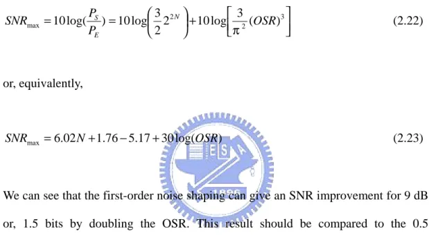
+ = = 3 2 2 max ( ) 3 log 10 2 2 3 log 10 ) log( 10 OSR P P SNR N E S π (2.22) or, equivalently, ) log( 30 17 . 5 76 . 1 02 . 6 max N OSR SNR = + − + (2.23)
We can see that the first-order noise shaping can give an SNR improvement for 9 dB
or, 1.5 bits by doubling the OSR. This result should be compared to the 0.5 bits/octave when oversampling with no noise shaping.
2.6.2 Second-Order Sigma-Delta Modulator
The second-order noise shaping SDM is shown in Figure 2.9. Through the
arrangement of the block diagram, we can obtain the noise transfer function, )
( f
NTF , as a second-order high-pass function
2 1 ) 1 ( ) (f = −z− NTF (2.24)
and the signal is just a delay to output. The signal transfer function is given by
1
) (f =z−
STF (2.25)
Combine two signal transfer function, we obtain the output as
) ( ) 1 ( ) ( ) (z z 1 U z z 1 2 E z Y = − ⋅ + − − ⋅ (2.26)
The same as before, we interest in the magnitude of the noise transfer function can
be show to given by 2 sin 2 ) ( = s TF f f f N π (2.27)
Integrate the quantization noise power over the frequency band of interest and use
the approximation, and result is given by
df f f f df f N f S P s s f f TF f f e e b b b b 4 2 2 2 sin 2 1 12 ) ( ) ( ∆ = =
∫
∫
− − π5 4 2 5 4 2 1 60 2 5 12 ∆ = ∆ ≅ OSR f f s b π π (2.28)
Again, assuming the maximum signal power is used, the maximum SNR for this case is given by + = = 5 4 2 max ( ) 5 log 10 2 2 3 log 10 ) log( 10 OSR P P SNR N E S π (2.29) or, equivalently, ) log( 50 9 . 12 76 . 1 02 . 6 max N OSR SNR = + − + (2.30)
We can see that the second-order noise shaping can give an SNR improvement for 15 dB or, 2.5 bits by doubling the OSR.
Compare with shape of zero-, first-, and second-order noise-shaping curves in
Figure 2.10. The noise power decreases as the noise-shaping order increases over the band of interest. But the out-of-band noise power increases for the higher-order
Second-order First-order Oversampling without noise shaping 0 fb fs/2 |NTF(f)|
Figure 2.10 Different order noise shaping curves
2.6.3 Higher-Order Sigma-Delta Modulator
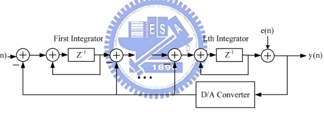
Figure 2.11 A simple block diagram of the second-order noise shaping SDM
In Figure 2.11, it shows the block diagram of the Lth-order SDM. We will discuss the behavior of the high-order SDM in mathematically. Now the noise
transfer function is given by
L
TF z z
N ( )=(1− −1) (2.31)
L s TF f f f N = 2sin π ) ( (2.32)
Integrate the quantization noise power over the frequency band of interest and use the approximation, and result is given by
df f f f df f N f S P L s s f f TF f f e e b b b b 2 2 2 2 sin 2 1 12 ) ( ) ( ∆ = =
∫
∫
− − π 1 2 2 2 1 2 2 2 1 ) 1 2 ( 12 2 1 2 12 + + + ⋅ ∆ = + ∆ ≅ L L L s b L OSR L f f L π π (2.33)Again, assuming the maximum signal power is used, the maximum SNR for this case is given by + + = = 2 +1 2 2 max ( ) 1 2 log 10 2 2 3 log 10 ) log( 10 N L L E S L OSR P P SNR π (2.34) or, equivalently, ) log( ) 10 20 ( 1 2 log 10 76 . 1 02 . 6 2 max L OSR L N SNR L + + + − + = π (2.35)
From equation (2.35) shows the information that we can improve SNR (6L+3) dB
(ie., resolution will increase L+0.5 bits) by doubling OSR, or improve SNR 6.02 dB (ie., resolution will increase 1 bit) by increasing the level of the quantizer.
2.6.4 Multi-Stage Sigma-Delta Modulator (MASH) (Cascaded)
There is a problem to improve SNR by increasing the order of the SDM. Modulators with more than two integrators suffer from potential instability owing to the accumulation of large signals in the integrators. Another approach for realizing
high-order modulators is to use a cascade-type structure where the overall higher-order modulators is constructed using lower-order ones. The advantage of this
approach is that since the lower-order modulators are more stable, the overall system should remain stable. Such an arrangement has been called MASH (Multi-stAge
noise SHaping) [5].
Figure 2.12 A second-order MASH modulator using two first-order modulators
The basic ideal is to pass along the quantization error of the first stage to another modulator and combine the outputs using digital filter. Then, the arrangement will
remove the quantization error of the first stage, and left only the second section’s quantization noise of the second stage which has been filtered twice.
A second-order MASH modulator using two first-order modulators is shown in
Figure 2.12. We can see that the output of the first stage is given by
) ( ) ( ) ( ) ( ) ( 1 1 1 z S z U z N z E z Y = TF + TF ) ( ) 1 ( ) ( 1 1 1 z E z z U z− + − − = (2.36)
and the output of the second stage is given by
) ( ) ( ) ( ) ( ) ( 2 1 2 2 2 z S z E z N z E z Y = TF + TF ) ( ) 1 ( ) ( 1 2 1 1 z E z z E z− + − − = (2.37)
Now we design the digital filter stage H and 1 H at the outputs of the two 2
modulators. The goal is to remove the quantization noise of the first stage, and this
can achieve if the condition
0 2 2 1 1⋅NTF −H ⋅NTF = H (2.38)
holds. The simplest choice for H1 and H2 are H1 =STF2 =z−1
and 2 1 (1 1)
−
− = = N z
H TF . The overall output is given by
) ( ) 1 ( ) ( ) ( 2 2 1 2 z E z z U z z Y = − − − − (2.39)
Thus, a MASH approach has the advantage that higher-order noise filtering can be
achieved using lower-order modulators. Since the lower-order modulator is robust, the overall MASH modulator is stable too. In similar way, we can apply this
2.6.5 System Analysis of Sigma-Delta Analog-to-Digital
Converters
The system architecture for typical oversampling ADC is shown in Figure 2.13. The analog domain includes anti-aliasing filter, sample-and-hold, and SDM. The
digital domain includes decimation filter which contains as digital low-pass filter and a down-sampling. The anti-aliasing filter is used to filter the out-of-band noise of
original input signal to avoid noise folding into signal band after sampled and held. Then, the sample-and-held transform the signal filtered from the anti-aliasing filter to
the signal which has the same value during sampling time, and its value is equal to the original signal at the moment when the sampling occurring. Next, SDM push the
quantization noise power to high frequency domain, and transform the output to digital domain. The digital low-pass filter will remove any higher-frequency signal
content that was originally on the input signal, and downsample the sampling frequency to Nyquist-rate. Note that the digital low-pass filter here is like an
anti-aliasing filter to limit signals to one-half the output sampling rate. The decimation filters generally are implemented using digital circuit technique in order
to reduce the power dissipation and are easy to implement. Figure 2.14 shows the signal and spectra of each stage of oversampling ADC [01]. There are example signal
spectra of an oversampling A/D converter with one bit quantizer in figure, and we can obtain more acquaintance with the overall system.
in
X (t) X (t)c X (t)sh Xdsm(n) X (n)lp X (n)s
Figure 2.13 Block diagram of an oversampling A/D converter
c X (t) sh X (t) 1 2 3 4 lp X (n) ± sdm X (n) = 1 1 2 3 s X (n) 1 2 3 c X (f) s f ω s X ( ) π 2π 4π 6π 8π 10π 12π ω f sh X (f) s f f ω sdm X ( ) ω 2π ω lp X ( ) ω 2π t n n n Time Frequency b f b f s b f f π 2 s b f f π 2
2.7 Digital Decimation Filter
Although there are many techniques for realizing digital decimation filters for oversampling A/D converter, we discuss the multi-stage decimation filters in this
section [01].
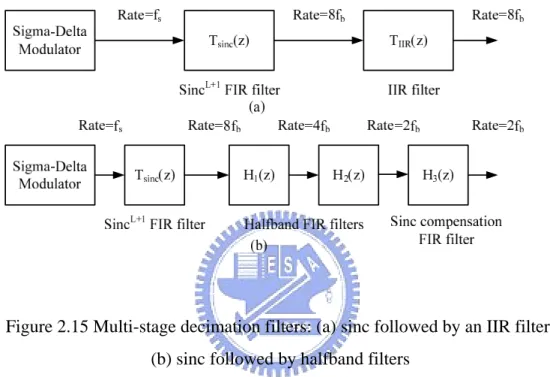
Figure 2.15 Multi-stage decimation filters: (a) sinc followed by an IIR filter; (b) sinc followed by halfband filters
One method for realizing decimation filters is to use a multi-stage approach, as shown in Figure 2.15. The first-stage SincL+1 FIR filter removes out of band
quantization noise and down sample the signal to four times the Nyquist rate. The second-stage can be an IIR filter or a cascade of FIR filters to down sample the output
of the first-stage to Nyquist rate. The first-stage SincL+1 FIR filter is a cascade of L+1 averaging filters where the transfer function of a single averaging filter, Tavg(z), is
given by
∑
− = − = = 1 0 1 ) ( ) ( ) ( M i i avg z M z U z Y z T (2.40)where M is the integer ratio of fs to 8 fb. Then, rewrite (2.40) we can see the frequency
response of an averaging filter, Tavg(z), is given by
) ( ) 1 ( ) ( ) ( 1 2 ( 1) 1 0 z U z z z z U z z MY M M i i − − − − − = − = + + + + =
∑
L (2.41)which can also be rewritten as
) ( ) 1 ( ) ( ) ( ) (z z 1 z 2 z U z z U z MY = − + − +L+ −M + − −M =Mz−1Y(z)+(1−z−M)U(z) (2.42) Finally, we group together Y(z) terms an find the transfer function of this averaging filter can also be written in the recursive form as
− − = = −−1 1 1 1 ) ( ) ( ) ( z z M z U z Y z T M avg (2.43)
The frequency response for this filter is found by substituting z = ejω, which results in
= 2 sin 2 sin ) ( ω ω ω c M c e Tavg j (2.44)
Where sinc(x) ≡ sin(x)/x.
1 1 1 sin 1 1 1 ) ( + − − + − − = L M L c z z M z T (2.45)
The reason for choosing to use L+1 of these averaging filters in cascade is similar to argument that the order of the analog low-pass filter in an oversampling D/A
converter should be higher than the order of the sigma-delta modulator. An efficient way to realize this cascade-of-averaging filter is to write (2.45) as
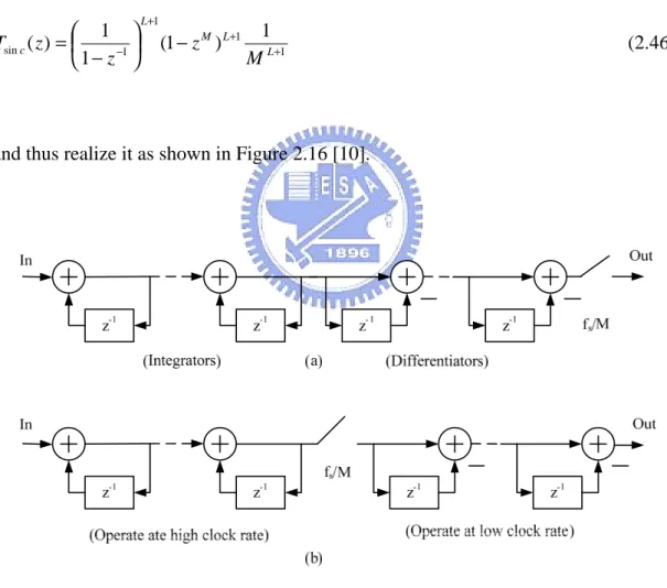
1 1 1 1 sin 1 ) 1 ( 1 1 ) ( + + + − − − = M L L L c M z z z T (2.46)
and thus realize it as shown in Figure 2.16 [10].
Figure 2.16 Realizing Tsinc(z) as a cascade of integrators and differentiators: (a) downsampling performed after all the filtering; (b) a more efficient method where
2.8 Summary
In this chapter, we have introduced the basic principles of sigma-delta modulator.
The advantages of the sigma-delta modulator are obtained form oversampling and noise shaping. By oversampling, the quantization noise is uniformly distributed over
2 /
s
f
± , and there is a little part of original quantization noise in our interesting bandwidth. Then, by feedback arrangement, noise shaping suppress the noise power
in signal bandwidth, and improve SNR. Here, various architectures of SDM such as single-loop and cascaded was introduced and compared. Besides, we discuss the
overall architecture of the oversampling A/D converter, and describe how the signals change in different sections. Subsequently, we give an example to show the signal
and spectra of each stage of oversampling ADC. Finally, we simply introduce the principle of the decimation filter. Now we get the common sense of the sigma-delta
Chapter 3 Basic Concept of Incremental ΔΣ
Converters
3.1 Introduction
For instrumentation application requiring high resolution and offset cancellation, the converters are mostly based on the dual-slope principle. The drawbacks of this
approach are the large external capacitors that are required for the integration of the input voltage and the relatively large conversion time [6]. Indeed, both are
exponentially increasing with resolution. In [7], a better implementation , called incremental A/D converter, has been proposed. The integration of the input signal and
of the voltage reference are mixed in time. This suppresses the need for large storage devices. An important feature of this converter is that it can achieve a very good offset
and 1/f noise cancellation. In this chapter, the theory and application of incremental ΔΣ converter will be introduced first. Second, high-order single loop incremental
and high-order MASH incremental will be discusses mathematically. Finally, the main problem of incremental ΔΣ converter are offset and charge injection problem, and
offset cancellation will be described.
3.2 Theory and application of incremental ΔΣ converter
The first-order incremental A/D converter represents a hybrid between a Nyquist-rate dual slope converter and a ΔΣ one [8]. Here, we will describe the
block diagram of the first-order incremental A/D converter including an integrator in
the loop, one-bit quantizer after integrator, and a digital counter at output. The main difference is that there the integration of the input and the reference is performed
separately, while here, they are alternating.
Figure 3.1 The block diagram of the first-order incremental A/D converter
We introduce the operation of this circuit step by step. Now we assume the input
signal close to DC, and nearly a constant DC level. At the beginning of the conversion, the integrator in the loop and the digital counter at output are both reset. We can set
the conversion time (n=2nbit) according to the required resolution (
bit
n ). For example,
if the required resolution is 6bit, the conversion time will be 26 steps. Whenever the
input to the quantizer exceeds zero, its output becomes 1, and −Vref is added to the input of the analog integrator. After n steps, the output of the integrator becomes
ref
in NV
nV
V = −
(3.1)
circuit is a feedback topology, the output of the integrator V must
satisfy−Vref <V <Vin, it follows that
ε + = ref in V V n N
(3.2)
where ε between -1 and 1. We can easily get the digital representation of the input signal N by a simple counter at the output of the modulator. Note that the residual
error at the output of the integrator is
ref qV
e
V =−2
(3.3)
where e between -0.5 and 0.5 is the quantization error of the conversion. For q
example, the input signal Vin =0.075Vref, resolution nbit =6bit, and the conversion time n=64 will be calculated. When the output of the integrator accumulates up to switch point, the output of the quantizer will becomes 1, and the input signal will be
minus Vref next step. After conversion, the digital representation of the input signal
N is 5.
The incremental converter is structurally similar to the conventional ΔΣ
converter, but there are significant differences: (1) the conversion is operated and realized in the form of discrete-time circuit; (2) both analog and digital integrators are reset before and after each conversion; (3) the decimating filter following the ΔΣ
counter).
3.3 High-order incremental converters
The biggest drawback of the first-order incremental A/D converter is that its conversion time is too long: for n -bit resolution, it needs 2n clock periods for each
conversion cycle. To reduce the number of cycles during one conversion, we can
increase the order of the incremental. The main purpose is to speed up the accumulation of the integrator. In [08], high-order single loop incremental converter
was described and in [9], the use of the two-stage (MASH) incremental converter was described. c1 c2 a3 b -b D/A Converter a2 a1
Reset Reset Reset
Vin Dout
Figure 3.2 A third-order cascaded-integrator/feed-forward modulator structure
First, we describe the high-order single loop incremental converter. The
operation will be discussed in terms of a third-order cascaded-integrator/feed-forward modulator structure shown in Figure 3.2. As in the first-order modulator, all memory
cycle. We use the notations of Figure, the output of all integrators can be found in the time domain after n clock cycles. The first integrator’s output samples are given by
) ] 0 [ ( ] 1 [ ] 2 [ ) ] 0 [ ( ] 1 [ 0 ] 0 [ 1 1 1 0 1 1 ref in i i ref in i i V d V b V V V d V b V V − + = − = =
M ) ] 1 [ ] 0 [ (Vin Vin d0Vref d1Vref b + − − =
∑
− = − = 1 0 1[ ] ( [ ] ) n k ref k in i n b V k dV V(3.4)
where dk =±1 is the quantizer output in the kth cycle.
similarly, the second integrator’s output samples are given by
[ ]
[ ]
2 [1] [1](
[1] [0])
0 ] 0 [ ] 0 [ 1 0 ] 0 [ 2 1 1 2 1 1 2 2 1 1 2 2 i i i i i i i i i V V c V V c V V V c V V + = + = = + = = M(
)
∑∑
∑
− = − = − = − = = 1 0 1 0 1 1 0 1 1 2[ ] [ ] [ ] n l l k ref k in n l i i n c V l cb V k d V V (3.5)and the third integrator’s output samples are given by
[ ]
[ ]
2 [1] [1](
[1] [0])
0 0 ] 0 [ 2 ] 0 [ ] 0 [ 1 0 ] 0 [ 2 2 2 3 2 2 3 2 3 2 2 3 3 = + = + = = = + = = i i i i i i i i i i V V c V V c V V c V V c V V M∑
− = = 1 0 2 2 3[ ] [ ] n m i i n c V m V
∑∑∑
(
)
− = − = − = − = 1 0 1 0 1 0 1 2 [ ] n m m l l k ref k in k d V V b c c (3.6)In the following, a constant V is assumed. In circuit design, it can be achieved by in
using sample-and-hold (S/H) circuit at the input of the converter. If the loop is stable
for all possible dc inputs, Vi3[n] will be bounded by ±Vref. Rearranging (3.6) and
assuming a constant V , we can get in
ref n m m l l k k in i V c cb d V n n n b c c n V
∑∑∑
− = − = − = − − − = 1 0 1 0 1 0 1 2 1 2 3 ! 3 ) 1 )( 2 ( ] [ (3.7)It is bounded by ±Vref, and we can get
ref ref n m m l l k k in ref V c cb d V V n n n b c c V < − − − < −
∑∑∑
− = − = − = 1 0 1 0 1 0 1 2 1 2 ! 3 ) 1 )( 2 ( (3.8)Rearrange (3.8) and compare with the equation
2 2 LSB LSB Vin LSB V V D Vin V < − < − we
common used in A/D converter, we can get
ref n m m l l k k ref in ref V n n n b c c d V n n n V V n n n b c c ( 2)( 1) ! 3 ) 1 )( 2 ( ! 3 ) 1 )( 2 ( ! 3 1 2 1 0 1 0 1 0 1 2 − − < − − − < − − −
∑∑∑
− = − = − = (3.9)Thus, after n clock periods, an estimate of V can be found as in
∑∑∑
− = − = − = − − = = 1 0 1 0 1 0 ) 1 )( 2 ( ! 3 ˆ n m m l l k k ref LSB Vin in V d n n n V D V (3.10)converter. Besides, we can find the equivalent value of the LSB voltage as ref LSB V n n n b c c V ) 1 )( 2 ( ! 3 1 2 − − = (3.11)
The relative quantization error (in LSBs) can also be found. It is given by
ref in n m m l l k k LSB in in q V V n n n b c c d b c c V V V e ! 3 ) 1 )( 2 ( 2 1 2 1 ˆ 2 1 1 0 1 0 1 0 2 1 − − − = − =
∑∑∑
− = − = − = (3.12) Hence, from (3.7) q ref i n V e V3[ ]=−2 (3.13)Thus, the quantization error can be found in analog form at the output of the last integrator. From (3.11), the equivalent number of bits (ENOB) can be derived as
− − = = ! 3 ) 1 )( 2 ( log 2 log2 2 c2c1b n n n V V n LSB ref bit 6 . 2 ) ( log ) ( log 3 2 + 2 1 2 − ≈ n ccb (3.14)
Where n >>1 was assumed.
In design, one needs to find the lowest value of n consistent with the required resolution. However, the scale factors cannot be chosen independently since they
affect the stability of the loop. We can choose these coefficients by computer to reduce the required conversion time and avoid overloading the integrators [08].
The derivations can easily be generalized to an arbitrary-order CIFF ΔΣ
modulator. The general expression is
∑ ∑ ∑
− = − = − = − = 1 0 1 0 1 0 ) 1 ( 2 1 1 n k k k k k k n L Vin L L L d C D L (3.15)Where L is the order of the analog loop.
D/A Converter D/A Converter Vin Reset Reset Digital Filter N2 ai bi Reset
Figure 3.3 The second-order 1-1 MASH incremental A/D converter
Since the high-order single loop incremental modulator have more than two integrators in the loop, their outputs can be very large and mush be limited, which is
not acceptable in the design of high-order incremental A/D converter. The high-order incremental modulator using MASH structure was proposed [08]. The second-order
modulator is ensured because there is only one integrator in each loop. The basic
operation is the same as the first-order incremental converter, and the main difference is that the first modulator delivers its output of the integrator to the input of the second
modulator. The signals continue to accumulate at the output of the integrator of the second modulator, and reduce the conversion time. Next, we will describe this
structure mathematically.
At the beginning of the conversion, the integrator in the loop and the digital counter at output are both reset. Assuming the input V is constant. In the first in
period, the output of the each integrator is given by
ref in i V aV V1[1]= − 1 (3.16) 0 ] 1 [ 2 = i V (3.17)
In the next period, the output of the each integrator is given by
ref in i V a a V V1[2]=2 −( 1+ 2) (3.18) ref ref in i V aV bV V2[2]= − 1 − 2 (3.19) ref in i V a a a V V1[3]=3 −( 1+ 2 + 3) (3.20) ref ref in i V a a V b b V V2[3]=3 −(2 1+ 2) −( 2+ 3) (3.21)
ref n i i in i n nV aV V
∑
= − = 1 1[ ] (3.22) ref n i i ref n i i in i n n nV a n iV bV V∑
∑
= − = − − − − = 2 1 1 2[ ] ( 1) /2 ( ) (3.23)and in the n +1 period, we can obtain
ref n i i ref n i i in i n n n V a n iV bV V
∑
∑
+ = = − − + − + = + 1 2 1 2[ 1] ( 1) /2 ( 1 ) (3.24)Again, it can be shown that the dynamic range of Vi2[n+1] is given by
ref i
ref V n V
V ≤ + ≤
− 2[ 1] (3.25)
with (3.24), (3.25) can be rewritten in the form of
ref ref n i i ref n i i in ref n n V a n iV bV V V ≤ + − + − − ≤ −
∑
∑
+ = = 1 2 1 ) 1 ( 2 / ) 1 ( (3.26) Rearranging (3.26) is given by ref ref n i i n i i in ref V n n V n n b i n a V V n n ( 1) 2 ) 1 ( 2 ) 1 ( ) 1 ( 2 1 2 1 + ≤ + + − + − ≤ + −∑
∑
+ = = (3.27)Compare with the ideal A/D converter quantization error is normally given by
2 2 LSB LSB Vin LSB Vin D V V V < − < − (3.28)
We can obtain the digital code of V in N , 2 VLSB, and resolution n as follow bit ref LSB V n n V ) 1 ( 4 + = (3.29) + − + =
∑
∑
+ = = 1 2 1 2 ( 1 ) n i i n i i n i b a N (3.30)[
( 1)]
1 log 2 log2 = 2 + − = n n V V n LSB ref bit 1 ) ( log 2 2 − = n if n >>1 (3.31)As an example, a 16-bit resolution, which requires from (3.31) that n =362.
An extra-bit accuracy can be obtained by detecting the sign of Vi2[n+1] at the end of the conversion cycle. This can be achieved without increasing significantly the conversion time. Equations (3.29)-(3.31) are replaced by
ref LSB V n n V ) 1 ( 2 + = (3.32) ]) 1 [ ( ) 1 ( 2 1 2 1 2 + + + − + =
∑
∑
+ = = p V sign b i n a N i n i i n i i (3.33)[
( 1)]
log2 + = n n nbit (3.34)Hence, for a 16-bit resolution, a total number of n+1=257 integration periods is required for each conversion cycle.
We can extended to a L th ( L >2) order incremental A/D converter. Due to the use of a multistage structure, there are no overload effects even if L >2. The resolution of