國
立 交 通 大 學
電信工程學系
博
士 論 文
微帶線高指向性耦合結構之研究與其應用
Research and applications of microstrip
coupled line structure with high directivity
研究生:王士鳴 (Shih-Ming Wang)
指導教授:張志揚 (Chi-Yang Chang)
微帶線高指向性耦合結構之研究與其應用
學生: 王士鳴 指導教授: 張志揚 博士
國立交通大學
電信工程學系
摘要
本論文主要在研究高指向性微帶結構及其應用。在論文的第一部
份,我們提出彎折式耦合線結構,其可有效地對偶模波速進行加速,
在適當設計下,可使奇偶模波速相等,而使耦合器具有高指向性的效
能。我們先設計出一個在極窄頻範圍內可達成極高指向性的耦合器,
再經由一些變化,可將其改變成一個在大頻寬範圍內皆具有高指向性
的耦合器。我們也將此結構應用在半波長帶通濾波器上,並且成功地
抑制了第一次諧振通帶。此結構的設計與合成過程在論文中有完整詳
細的說明。在論文的第二部份,提出了一種設計架構,能有效縮小微
帶平行弱耦合器的面積,並保有高指向性的效能。
Research and applications of microstrip
coupled line structure with high directivity
Student: Shih-Ming Wang Advisor: Dr. Chi-Yang Chang
Department of Communication Engineering
National Chiao Tung University
Abstract
This dissertation presents the research and applications of microstrip
coupler with high directivity. In the first part, we proposed a meandered
parallel-coupled line. It can speed up the even-mode phase velocity and
make the modal phase velocities to be equal in microstrip structure.
Therefore, we can get a good directivity in microstrip parallel-coupled
coupler. With proper design, we can get an ultra high directivity in a
narrow band or get a high directivity performance over broad bandwidth.
We also apply the proposed structure to a half wavelength band pass filter
and successfully cancel the first spurious passband. All the synthesis
procedures of the proposed structure are described in detail. The second
part presents a solution for miniaturizing microstrip loose coupler with
high directivity.
誌謝
首先要感謝張志揚教授在這幾年來辛勤與耐心的指導,其觀念啟
發以及適當的協助帶我走出研究上的迷惘,也使本研究得以完成。另
外也感謝口試委員陳俊雄教授、吳瑞北教授、鍾世忠教授、郭仁財教
授與楊正任教授對本研究所給予的指正與建議。
這裡還要特別感謝微波薄膜實驗室的學弟謝明諭與紀鈞翔,無論
是在研究討論或是生活減壓上給予的幫助。另外,對於曾幫助過我的
實驗室學長、姐、弟、妹在此一併誌謝。
接下來,還要感謝我在美國交換研究期間的指導教授林仁山教授
對我在待人與研究精神上的另類啟發。也感謝在美國認識,曾給予我
各項協助與研究打氣的好朋友們,讓我在美國的生活充實且快樂。
最後在此感謝我的家人與女友昱璇在我背後默默地給予我在經
濟上與精神上的支持與鼓勵,謝謝你們!
士鳴
2005 年九月於台灣新竹
Contents
Abstract (Chinese)………I Abstract ...…………...………...II Acknowledgement………Ⅲ Contents………...…IV List of Tables……..………...………...……VI List of Figures……….….…………...………...…...…….….VII 1 Introduction………...………..…….….….1 1.1 Brief History …………..………...…….…………...….1 1.2 Research Motives………...…………..…………...…3 1.3 Literature Survey………..………..………...4 1.4 Contribution………...…...…..7 1.5 Chapter Outline ………...………...….72 Characteristics of microstrip parallel-coupled line………...9
2.1The characteristic of microstrip parallel-coupled line….………...…9
2.2 The necessary conditions of high directivity coupler.…....…………...……. 14
parallel-coupled line………..……….….21
3.1 The characteristics of meandered parallel-coupled line ……...….21
3.2 Synthesis of meandered parallel-coupled line…………..………….…...…28
3.3 Coupler with ultra high directivity within a narrow band………...29
3.4 Coupler with high directivity over broad bandwidth………...…..…..38
4 Analysis, design and realization of band pass filter with meandered parallel-coupled line………...….43
4.1 Previous works for removing spurious passband..……….………….….44
4.2 The mechanism of modified MPCL to suppress spurious passband…….…...45
4.3 Filter design………...………..………49
4.4 Simulation and measurement responses………...…..….52
4.5 Discussion………..………..……….…...58
5 Analysis, design and realization of miniaturized loose coupler with high directivity………...……….…..60
5.1 The placement of grounded strip………...……….……….61
5.2 Procedures of implementation………..………...63
5.3 Simulation and measurement………....………..……….66
5.4 Discussion………..………..……….…...69
6 Conclusion……….………...………..71
6.1 Measured parallel-coupled line………...……….…………...….71
6.2 Miniaturized loose coupler………….………..………...72
6.2 Review and the future works………….………..………….………...73
List of Tables
Table 4.1 Filter design parameters.………...……….………...…...53 Table 5.2 The designed parameters of proposed couplers.………….………...…...66
List of Figures
Figure 1.1 The first directional coupler using a quarter-wave-long two-wire configuration………...……...………….2 Figure 1.2 The first TEM-mode quarter-wavelength parallel-line backward coupler with clear description with formulas…………...…………..………3 Figure 1.3 Lumped capacitor compensation of microstrip coupler………….……....5 Figure 1.4 Parallel-coupled microstrip with dielectric overlay compensation……....6 Figure 1.5 Wiggly two-line coupler…..………..………...….6 Figure 2.1 The structure of microstrip coupler………..11 Figure 2.2 Cross section of symmetrical microstrip coupler…………...…..……....11 Figure 2.3 (a) The electrical field distribution and (b) capacitance representation of one-half of the structure for even-mode excitation, (c) The electrical field distribution and (d) capacitance representation of one-half of the structure for odd-mode excitation…….….………..……...……12 Figure 2.4 The schematic circuit of microstrip coupler………....15 Figure 2.5 The decomposition of coupled line coupler circuit of Figure 2.3 into
even-mode and odd-mode excitations. (a) Even mode. (b) Odd mode…15 Figure 2.6 Equivalent circuit for determining scattering matrix of the (a) Even mode.
(b) Odd mode……….………..16 Figure 3.1 A standard meandered parallel line………...22 Figure 3.2 Schiffman section. (a) The schematic representation. (b) The dispersive phase responses…..………..………...….23 Figure 3.3 The even- and the odd-mode characteristic impedances with different normalized meandered distance on (a) a 50mil-thick Rogers RT6010
substrate and (b) a 20mil-thick Rogers RO4003 substrate………..25 Figure 3.4 A standard meandered parallel line in HFSS…………...…...…..…....26 Figure 3.5 (a) The even- and (b) the odd-mode electrical fields in the
cross-section……….27 Figure 3.6 The even- and the odd-mode transmission phases (at 2 GHz) with
different normalized meandered distance on (a) a 50mil-thick Rogers RT6010 substrate and (b) a 20mil-thick Rogers RO4003 substrate…..………..………...……...….28 Figure 3.7 The modal transmission phases of single section meandered
parallel-coupled line……….…………..30 Figure 3.8 The simulated and measured return losses of the single section
meandered parallel-coupled line…………...…..……….…....31 Figure 3.9 The simulated and measured couplings of the single section meandered parallel-coupled line………...31 Figure 3.10 The simulated and measured isolations of the single section meandered parallel-coupled line..………..………...….32 Figure 3.11 The simulated and measured directivities of the single section meandered parallel-coupled line………..……..32 Figure 3.12 The (a) layout and (b) photograph of the coupler with ultra high
directivity…………...…..………..…....35 Figure 3.13 (a) The simplified equivalent circuit of Figure 3.1 (b) the simplified
equivalent of (a) in even mode excitation. (Unit: mils)………..36 Figure 3.14 The port matching responses and transmission phases of the equivalent circuits in Figure 3.13 with (a) theoretical Zi and (b) tuned
Zi.…..………..………...….37
Figure 3.16 (a) The multisection meandered parallel-coupled line. (b) The unit-meandered-section………..39 Figure 3.17 The modal transmission phases of conventional parallel-coupled-line
coupler and the even-mode transmission phase with single, two, and five meandered sections…………...………..……....40 Figure 3.18 The simulated and measured return loss and coupling of the proposed coupler………....41 Figure 3.19 The simulated and measured isolation of the proposed coupler and
measured isolation of a conventional coupler with the same specification…..………..………...…………...….41 Figure 3.20 The layout of the proposed coupler……….………..42 Figure 3.21 The circuit size comparison between proposed and conventional c o u p l e r … … … … . . . … . . … … . . . . 4 2 Figure 4.1 A TEM parallel-coupled bandpass section. (a) The schematic
representation. (b) The equivalent circuit………...46 Figure 4.2 (a) The conventional parallel-coupled line. (b) The proposed meandered parallel coupled line…..………..……….…...….47 Figure 4.3 The modal transmission phases of a conventional parallel-coupled line and a coupled Schiffman section with different coupled line length. For l = L/2, : θo, : θe without Schiffman effect, : θe with Schiffman effect.
For l < L/2, : θo, : θe without Schiffman effect, : θe with Schiffman effect……….………..48 Figure 4.4 The even-mode and odd-mode transmission phases of a
conventional parallel-coupled line, and two different solutions , and of meandered parallel coupled lines with equal modal transmission phases at 2fo.…………...…..………...…....48
Figure 4.5 The design plots of the meandered parallel coupled line with b = 60 mil. (a) The corresponding meandered distance d and coupled-Schiffman section length l. (b) The even- and odd-mode characteristic impedances versus w/h and s/h of meandered parallel-coupled line………...51 Figure 4.6 (a)The simulated and measured responses of filter A and the measured insertion loss of conventional filter with the same specification is compared. (b) The simulated and measured responses of filter B. (c) The simulated and measured responses of filter C…..………...….55 Figure 4.7 The layout of (a) Filter A. (b) Filter B. (c) Filter C………...…………..56 Figure 4.8 The photograph of (a) Filter A. (b) Filter B. (c) Filter……….…....58 Figure 4.9 The circuit size comparison between filter A and conventional filter….58 Figure 5.1 Coupled lines with a grounded strip insertion…..………...…...….62 Figure 5.2 Coupled lines with a modified grounded strip………...…..62 Figure 5.3 The grounding effect is induced by (a) λ/4 open stub and (b) wrap-around grounding strips…………...……….……....63 Figure 5.4 An interdigital capacitor………...65 Figure 5.5 The extraction of initial physical dimensions of coupler in circuit
simulator…..………..………...………...….65 Figure 5.6 The (a) simulated and (b) measured responses of 30-dB coupler………67 Figure 5.7 The (a) simulated and (b) measured responses of 40-dB coupler……....68 Figure 5.8 The photographs of (a) 30-dB and (b) 40-dB coupler………...69
Chapter 1
Introduction
Microwave transmission lines are normally classified as two types: (1) to carry information or energy from one point to another; (2) as circuit element for passive circuits like couplers, baluns, filters, resonators, and impedance transformers. In microwave circuits, passive elements mainly consist of distributed type and employ transmission line sections and waveguides in different configurations and to achieve the desired specifications. The functionality is largely achieved by the use of coupled transmission lines. In which, microstrip coupled lines are popular due to the low cost and easy fabrication. However, the inherent disadvantage of poor directivity destroys the performances of the coupler itself and limits the feasibility in various extended applications. In this chapter, we briefly describe the original of coupled lines, the significance of high directivity, previous works for directivity improvement, and our proposal and contributions.
1.1 Brief History
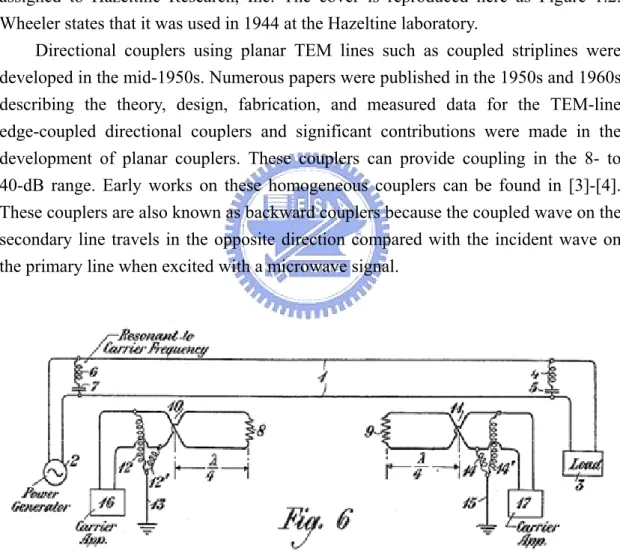
The exact beginnings of directional couplers using parallel wires are not clear. Such couplers were used for various applications before any of the modern theories or design data were available. The first directional coupler using a quarter-wave-long two-wire configuration, U.S. Patent 1,615,896, entitled “High Frequency Signaling System” [1] was filed in 1922 and granted in 1927 to Herman A. Affel, and assigned
to American Telephone and Telegraph Company. Affel refers to a ”loop antenna”, which is shown in Figure 1.1 consists of a two-wire transmission line quarter-wavelength long, with a resistive termination at one end and a detector at the other end. This quarter-wavelength line which was called loop antenna is parallel to another longer two-wire transmission line, and could work like a directional coupler at midband of properly design. However, it is not explicitly referred to as a directional coupler.
A clear description with formulas of a TEM-mode quarter-wavelength parallel-line backward coupler was filed in U.S. Patent 2,606,974, entitled “Directional Coupler” [2] in 1946, and granted in 1952 to Harold A. Wheeler, being assigned to Hazeltine Research, Inc. The cover is reproduced here as Figure 1.2. Wheeler states that it was used in 1944 at the Hazeltine laboratory.
Directional couplers using planar TEM lines such as coupled striplines were developed in the mid-1950s. Numerous papers were published in the 1950s and 1960s describing the theory, design, fabrication, and measured data for the TEM-line edge-coupled directional couplers and significant contributions were made in the development of planar couplers. These couplers can provide coupling in the 8- to 40-dB range. Early works on these homogeneous couplers can be found in [3]-[4]. These couplers are also known as backward couplers because the coupled wave on the secondary line travels in the opposite direction compared with the incident wave on the primary line when excited with a microwave signal.
Figure 1.1 The first directional coupler using a quarter-wave-long two-wire configuration.
Figure 1.2 The first TEM-mode quarter-wavelength parallel-line backward coupler with clear description with formulas.
1.2 Research Motivations
Microstrip coupling structure has become very popular due to insensitivity to fabrication tolerance and simple synthesis procedures. Its planar structure allows laying solid-state devices and lumped elements on its surface. Microstrip coupling structure can be used to design many various microwave circuits, such as directional coupler, edge-coupled line filter, balun, delay line, dc block, interdigital capacitor, spiral inductor, coupled-line impedance transformer, and spiral transformer. And it also frequently appears in high-speed digital signal printed circuit board and in many microwave measurement systems.
However, based on its semi-open structure, the electromagnetic field distributes in both air and dielectric region, and the propagation mode is quasi TEM. Due to the inhomogeneous material that results the odd-mode phase velocity commonly faster than the even-mode value, in another word, that causes the odd-mode transmission phase smaller than the even-mode value. The inequality of modal phase velocities (and transmission phases) will degrade the isolation or directivity performance of the microstrip coupled-line structure. The performances of many of the microwave circuits mentioned above degrade because of poor directivity. For a backward-wave directional coupler, the coupling value might change, as the coupler isolation is not very good and in the mean time the coupler is not well terminated. For a Machand type balun, the balance of amplitude and/or phase degrade due to poor directivity. For a coupled-line bandpass filter, extra spurious passband appears and it might make the upper stopband performance get worse. For some of other circuits, the parasitic effects might cause undesirable performances. Therefore, a microstrip coupled-line structure with good isolation is important for various microwave circuits design.
The second problem encountered in the microstrip coupled-line coupler is that as the coupling gets loose, two lines of convention coupler becomes wider spaced. That makes the coupler not only occupies more circuit area but also has very poor directivity. Because of the large line spacing, the capacitor compensation of phase velocity becomes very difficult. In addition, in order to get a near-constant coupling over a wider frequency bandwidth, a multisection coupler that consists of a number of single-section couplers with tight and loose coupling is commonly used. However, the different coupling has different spacing between the two coupled lines for each section of coupler. This means that the discontinuities certainly exist in the junctions of different single-section couplers, even if the small lengths of tapered transmission lines are used. In higher frequency, these discontinuities will produce extra reactance and lengths and then degrade the input matching and directivity. Therefore, a loose coupler with narrower coupled-line spacing is needed for reducing the discontinuities. Besides, the directivity of a single-section coupler is more important in multisection coupler application. The unequal phase velocities will get poor directivity and make the coupling to be inaccurate especially when the whole coupled line length get longer. So, a loose coupler with narrower coupled-line spacing and high directivity is necessary for a multisection coupler.
The purpose of this research is to find some methods to solve the above-described problems.
1.3 Literature Survey
For improving the directivity of the microstrip coupled-line coupler, there are many early works are proposed to equalize or compensate of unequal modal phase velocities (and modal transmission phases). Basically, methods to solve this problem can be summarized in three major groups. The first method is shown in Figure 1.3. By adding single or multiple lumped elements at the end or the center of the coupler, the odd-mode phase velocity slows down due to the raise of the odd-mode effective dielectric constant [5]-[9]. On the other hand, the lumped elements are nearly invisible in the even mode. The initial synthesis procedures and the achievable coupling range of this compensated method are the same as conventional coupler. Moreover, it is effective to get high directivity in a wide bandwidth. However, the value of lumped component should be calculated and length of coupled section should be shortened due to the odd-mode phase velocity slows down. Although [5]-[7] provide the formulas for calculating the value of lumped element and shortened length, in practice, the available lumped element value usually does not meet the exact value and the lumped component usually shows parasitic effects as the frequency goes high.
Distributed component is, therefore, a good solution to implement the lumped element in high frequency.
W
S
L
C
1C
2Figure 1.3 Lumped capacitor compensation of microstrip coupler.
The second method is shown as Figure 1.4. By placing one or more additional dielectric layers with proper thickness and dielectric constant on top of microstrip coupler, the odd-mode phase velocity can be slowed down due to the increase of odd-mode effective dielectric constant, and can be equaled to the even-mode value [10]-[15]. This thought is straight forward and it can shorten the circuit size by show-wave effect. Furthermore, it makes the realization of tight coupling easier with the same lines spacing. However, it’s not a planar structure anymore and adding any additional material needs extra cost and process. Moreover, due to the variation of dielectric environment, the line width and line spacing are different from the initial dimensions of microstrip coupler and need to be recalculated. Unfortunately, there are no mature synthesis formulas for various dielectric environments. To obtain most of the dimensions require some special design charts and need electro-magnetic field analysis to calculate the characteristics of the proposed special structure. This kind of design is more complicated and time-consuming. The most important drawback is that the design results fit case-by-case and common solution is difficult to obtain.
The third method is shown in Figure 1.5 that the inner edges of a pair of microstrip lines are changed to wiggle or serpentining or slot shape [16]-[20]. Since most of the odd-mode current is propagated along the inner edge, the effective propagating length of the odd-mode signal is increased so that the propagating phase of odd-mode can be equaled to that of the even-mode signal. The circuit structure is pure planar and the slow wave-like effect can effectively shorten the physical length of the circuit. However, the design begins with Fourier transform analysis, and the
synthesized structure is optimized using iterative techniques [20]. These steps cannot be implemented in standard simulators, and the whole process is rather time-consuming. Besides, the unsmooth inner edge not only makes the high order propagating mode easily to be excited but also increases the insertion loss. Moreover, the odd-mode inductance per unit length increases, as the variation of inner edge gets more drastic. That means the odd-mode characteristic impedance increases and results in a looser coupling as comparing to the conventional coupled lines with the same line spacing.
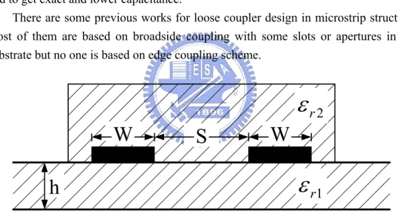
For improving the directivity of loosely coupled microstrip lines, few works have been done on this topic. As [21] indicates, it’s not appropriate to add lump capacitor on the two ends of a loose coupler due to the wide coupled line spacing and only very small compensated capacitance is needed. Conventional lump capacitor is hard to get exact and such a low capacitance value. In the contrary, interdigital capacitor is good for this kind of application, because it is easier to fit the wide coupled-line spacing and to get exact and lower capacitance.
There are some previous works for loose coupler design in microstrip structure, most of them are based on broadside coupling with some slots or apertures in the substrate but no one is based on edge coupling scheme.
1 r
ε
2 rε
Figure 1.4 Parallel-coupled microstrip with dielectric overlay compensation.
1.4 Contribution
Comparing to the various methods for directivity improvement described in section 1.3, this dissertation proposes the structure of meandered parallel-coupled line. The even-mode phase velocity can be speeded up by meandering the parallel-coupled line. Proper meandering equals the even- and the odd-mode phase velocities and achieves high directivity. By the single section meandered parallel-coupled lines, we can locate high directivity performance at any narrow frequency band that we want. Furthermore, the frequency band with high directivity can be wider by dividing the coupled line in to multiple sections of cascaded meandered parallel-coupled lines. In addition, the proposed structure, based on the characteristic of meandering, can effectively miniaturize the circuit for all of its applications, especially in higher order filter design. In practical fabrication, no addition component, material, and process are needed, thus, low fabrication cost can be kept.
In another part of this dissertation, a miniaturized high directivity loose microstrip coupler is proposed. We place a grounded strip between the two parallel-coupled lines to block the coupling and place two interdigital capacitors in both ends of the coupler to improve the directivity. The design procedures and consideration will be discussed in detail.
1.5 Chapter outline
In this dissertation, Chapter 1 is the introduction, which describes the original of parallel-coupled lines and the importance of the directivity. A brief description of the proposed methods is provided with comparison of various previous works. Chapter 2 describes the inherent characteristics and disadvantages of microstrip parallel-coupled lines, and derives the scattering parameters to obtain the necessary conditions for high directivity in the basis of Quasi-TEM mode. Chapter 3 describes the motivation of using the meandered parallel-coupled lines and the characteristics of this kind of parallel-coupled line. Moreover, it also describes the procedures to synthesis the proposed meandered parallel-coupled lines by commercial CAD tools in detail. Then, based on the proposed structure, two couplers are designed and demonstrated with narrow-band and wide-band high directivity performance, respectively. Chapter 4 uses the characteristics of the proposed meandered parallel-coupled lines to design a bandpass filter not only eliminating the spurious passband near twice of the center frequency but also drastically shrinking the circuit size. In this chapter, the design procedures and information are described in detail for this kind of filter. Chapter 5
describes the design of the miniaturized loosely coupled parallel-coupled line coupler with high directivity. Chapter 6 gives the conclusion.
Chapter 2
Theory of the microstrip parallel
coupled line coupler
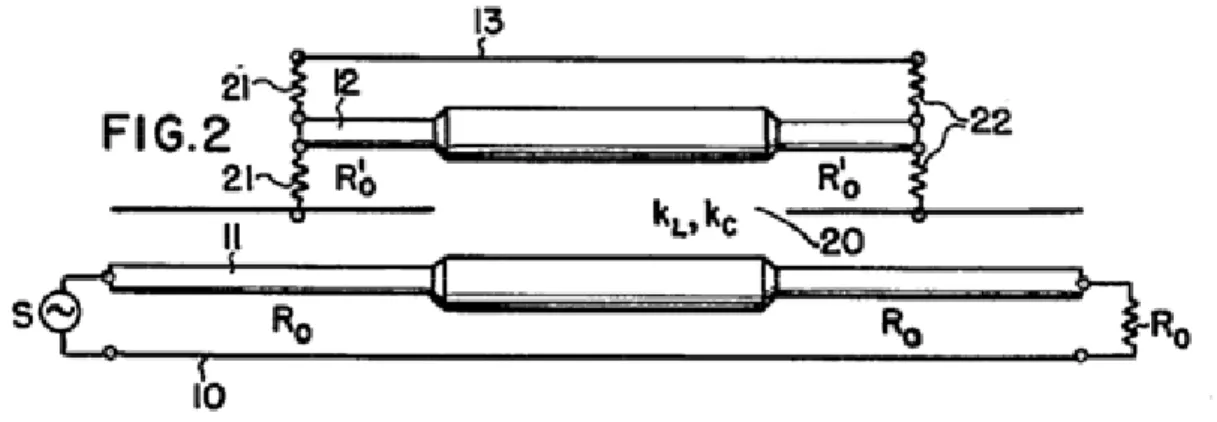
Transmission lines used at microwave frequencies can be briefly divided into two categories: TEM (or Quasi-TEM) mode transmission lines and non-TEM transmission lines. When a signal propagates on a microstrip structure, because the electromagnetic fields are distributed in an inhomogeneous material, the propagation mode is Quasi-TEM. For a symmetric TEM or Quasi-TEM coupled transmission lines, the determination of important electrical characteristics (such as modal characteristic impedances and phase velocities) of coupled lines reduces to finding the modal capacitances associated with the structure and excitation mode. This chapter discusses the general characteristics of symmetric microstrip parallel coupled lines and also gives the design equations. In addition, the scattering parameters of microstrip parallel coupled lines based on Quasi-TEM mode are derived without the constrain of equal modal phase velocities and the necessary conditions for high directivity is also discussed. Finally, some practical suggestions are given for designing a high-directivity microstrip coupler.
2.1 The characteristic of microstrip parallel coupled line
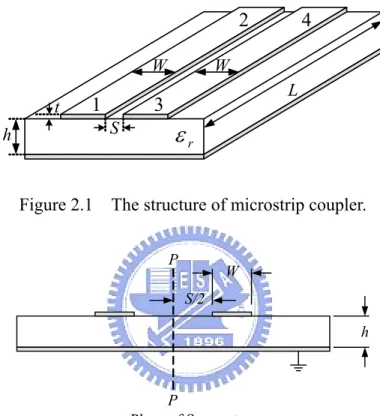
propagating on each line interferes each other. Coupler is an application based on this scheme. The physical structure of a microstrip coupler is shown in Figure 2.1, where
h and εr are the thickness and dielectric constant of substrate, respectively, t is the
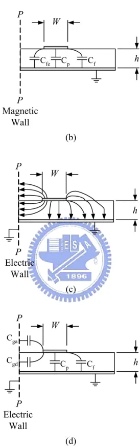
thickness of conductor, W is the coupled line width, S is the spacing between coupled line, and L is coupled line length. Figure 2.2 is the cross sectional view of the microstrip coupled lines. The structure can be analyzed by even- and odd-mode excitation. The even-mode electrical field distribution of one-half of the structure is shown in Figure 2.3(a). In this case, both lines are driven in phase from equal source of equal impedance and voltage, and the impedance from one line to ground in even-mode excitation can be defined as the even-mode characteristic impedance, Z0e.
Since the electrical fields between both coupled lines are parallel to the symmetric plane of the circuit, the normal component of the electric field at PP’ plane is zero. It can be imaged a magnetic wall (M-wall) exists on the symmetric plane PP’ and it is effectively an open-circuit on that plane. The even-mode capacitance of either of the coupled lines, which can be represented as shown in Figure 2.3(b), is given by,
e p f fe
C =C +C +C (2.1)
The capacitance that results from the electrical field in the region directly below the strip is known as the parallel-plate capacitance Cp, while that resulting from the
fringing fields in the outer edge is known as the fringing capacitance Cf. Cfe means the
fringing capacitance in the inner edge of coupled lines, which is different from Cf,
because the inner edge has a M-wall near by.
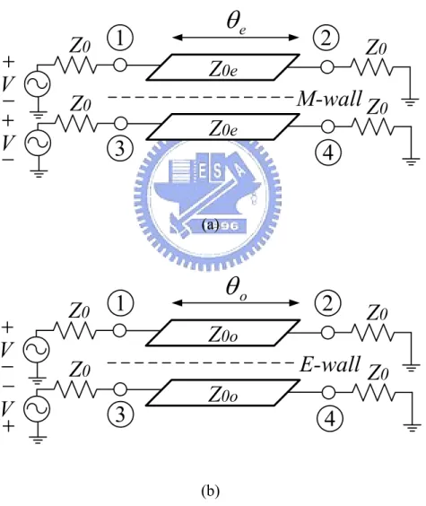
The electrical field distribution of one-half of the coupled structure is shown in Figure 2.3(c) for odd-mode excitation. In this case, both lines are driven out of phase from equal source of equal impedance and voltage, and the impedance from one line to ground in odd-mode excitation can be defined as the odd-mode characteristic impedance, Z0o. Since the electrical fields between both coupled lines are
perpendicular to the symmetric plane of the circuit, it can be imaged an electric wall (E-wall) exists on the symmetric plane PP’ and the voltage on it is zero. Because PP’
is an E-wall the tangential electric field on it should be zero. The odd-mode capacitance of either of the coupled lines is given by
o p f fo
C =C +C +C (2.2)
which is assumed to consist of two capacitances Cga and Cgd in parallel; that is,
fo ga gd
C =C +C (2.3)
where Cga and Cgd are the capacitances corresponding to the fringing field between
the inner edges exist in the air and dielectric regions, respectively.
r
ε
h W W S 1 2 3 4 t LFigure 2.1 The structure of microstrip coupler.
P P W h Plane of Symmetry S/2
Figure 2.2 Cross section of symmetrical microstrip coupler.
P
P
W
h
Magnetic
Wall
(a)P W h Cp Cf Cfe P Magnetic Wall (b) P P W h Electric Wall (c) P W h Cp Cf P Electric Wall Cgd Cga (d)
Figure 2.3 (a) The electrical field distribution and (b) capacitance representation of one-half of the structure for even-mode excitation, (c) The electrical field distribution and (d) capacitance representation of one-half of the structure for odd-mode excitation.
The definitions of the even- and the odd-mod effective dielectric constant are 2 2 _ / e e r eff c V p ε = (2.4a) 2 2 _ / o o r eff c V p ε = (2.4b)
where c is the speed of light in free space, and Vep and Vop are the even- and the
odd-mode phase velocity, respectively. In Figure 2.2, the effective dielectric constants take into account the relative distribution of electric field in the various regions of the inhomogeneous medium. Besides, the effective dielectric constants are a function of frequency and strictly speaking should be evaluated using equation (2.4) where the phase velocity is compute by using some rigorous method based on Maxwell’s equations. However, on the quasi-static assumption, the even- and odd-mode effective dielectric constant can be defined as fellows:
_ / 1 e r eff C Ce e ε = (2.5a) o _ / 1 r eff C Co o ε = (2.5b)
where Ce1 and Co1 denote the modal capacitances between the same conductor in a
homogeneous dielectric medium of unity dielectric constant. In order to get the sense for the even- and odd-mode dielectric constant, let us refer to Figure 2.3 (a) and (c), which show the even- and odd-mode electrical field distributions of a microstrip parallel coupled line. The figures indicate that the relative E-field distributions in air and substrate region are different for the two modes, and the odd-mode electrical field has more relative distributions in the air region. It implies that the εor_eff is smaller than
εer_eff and Vop is faster than Vep by equation (2.4).
The transmission phases of both modes are
e e p L V ω θ = (2.6a) o o p L V ω θ = (2.6b)
coupled line.
The even- and odd-mode characteristic impedance are given by
0 1 e e e p Z C V = (2.7a) 0o 1o o p Z C V = (2.7b)
The detailed analysis formulas for even- and odd-mode characteristic impedance in microstrip coupled lines can refer to [22].
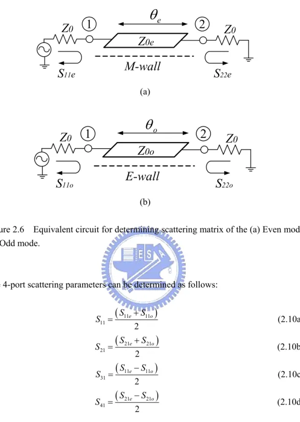
2.2 The necessary conditions of a high directivity coupler
Figure 2.4 is the schematic circuit of microstrip coupler. Because of symmetry, the excitation in Figure 2.4 can be decomposed into even-mode and odd-mode excitations as shown in Figure 2.5(a) and (b), respectively. In order to analysis easily, the schematic circuits on Figure 2.5(a) and (b) can be simplified as shown in Figure 2.6 (a) and (b) which are two-ports circuit with characteristic impedance Z0e and Z0o,
transmission phase θe and θo, respectively. Since the even- and odd-mode circuits are
two-port network, the ABCD matrix for the even- and odd-mode are given, respectively, by 0 0 sin sin cos e e e e e e e e e e A B cos jZ C D jY θ θ θ θ = (2.8a) 0 0 sin sin cos o o o o o o o o o o A B cos jZ C D jY θ θ θ θ = (2.8b)
And then transfer the ABCD matrix to scattering matrix, we obtain
[ ]
11 12 21 22 e e e e e S S S S S = (2.9a)[ ]
11 12 21 22 o o o o o S S S S S = (2.9b)Z
0e, Z
0o e oθ
θ
,
Z
0Z
0Z
0Z
02V
1
3
2
4
Figure 2.4 The schematic circuit of microstrip coupler.
e
θ
Z0
Z
0Z0
Z0
V
V
Z
0eZ0e
M-wall
1
3
2
4
(a) oθ
Z
0Z
0Z
0Z
0V
V
Z
0oZ
0oE-wall
1
3
2
4
(b)Figure 2.5 The decomposition of coupled line coupler circuit of Figure 2.3 into even-mode and odd-mode excitations. (a) Even mode. (b) Odd mode.
e
θ
Z
0Z
0Z
0eM-wall
S
11eS
22e1
2
(a) oθ
Z
0Z
0Z
0oE-wall
S
11oS
22o1
2
(b)Figure 2.6 Equivalent circuit for determining scattering matrix of the (a) Even mode. (b) Odd mode.
The 4-port scattering parameters can be determined as follows:
(
11 11)
11 2 e o S S S = + (2.10a)(
21 21)
21 2 e o S S S = + (2.10b)(
11 11)
31 2 e o S S S = − (2.10c)(
21 21)
41 2 e o S S S = − (2.10d)Since the structure of microstrip coupler is symmetric, the four scattering parameters shown in (2.10) can represent the whole scattering matrix of microstrip coupler. The equation (2.10a), (2.10b), (2.10c), and (2.10d) are the return loss, through, coupling and isolation of a coupler, respectively. Finally, the return loss of microstrip coupler in equation (2.10a) can be derived as
2 2 4 2 2 2 2 0 0 0 0 0 0 0 0 0 0 0 0 11 2 2 2 2
0 0 0 0 0 0 0 0
( )sin sin ( ) cos sin ( ) cos sin [( )sin 2 cos ][( )sin 2 cos ]
e o e o e e o e o o o e o e e e e e o o o o Z Z Z jZ Z Z Z Z Z Z Z Z S Z Z jZ Z Z Z jZ Z θ θ θ θ θ θ θ θ θ θ − + − + − = + − + − (2.11)
To make a matched coupler the numerator of equation (2.11) should be zero. We can firstly obtain the necessary condition to make the real part of numerator in equation (2.11) to be zero. That is
0 0e 0o
Z = Z Z (2.12)
With (2.12), the imaginary part of numerator in equation (2.11) can be derived as
2 2 2 2 0 0 0 0 0 0 0
(Z Ze o−Z Ze o ) cos sinθe θo+(Z e −Z Zo e ) cos sinθo θe (2.13)
and in microstrip coupler, the even-mode transmission phase is always larger than that of the odd mode. Thus, we can set
2 o e θ θ θ = + (2.14) / 2 e θ = + ∆θ θ (2.15a) / 2 o θ = − ∆θ θ (2.15b) where ∆θ is a small phase difference because θe and θo are close to each other. Then
cosθo, sinθo, cosθe, and sinθe can be expanded as, respectively
cosθo =cos cosθ ∆θ/ 2 sin sin+ θ ∆θ/ 2 (2.16a) sinθo =sin cosθ ∆θ/ 2 cos sin− θ ∆θ/ 2 (2.16b) cosθe =cos cosθ ∆θ / 2 sin sin− θ ∆θ / 2 (2.16c) sinθe =sin cosθ ∆θ/ 2 cos sin+ θ ∆θ/ 2 (2.16d)
After substituting equation (2.12) and (2.16) to equation (2.13), the imaginary part of numerator of return loss will exactly equal to
2 0 0 0 2sin cos ( ) 2 2 Z Z e Z o θ θ ∆ ∆ − − (2.17)
because Z0 and cos(∆θ/2) is impossible to be zero (∆θ is supposed to be a small phase
difference) and it’s not meaningful for Z0e and Z0o equal in a coupler, we know ∆θ=0
is another necessary condition for S11=0. In practical application, the S11 will not too
bed even though the phase difference between the two modes is over 30%. That indicates ∆θ=0, in theatrically, is a necessary condition, but not a real important condition for well matching in practically.
The through of microstrip coupler in equation (2.10b) can be derived as
0 0 0 0
21 2 2 2 2
0 0 0 0 0 0 0 0
2 cos ( )sin 2 cos ( )sin
e o e e e e o o o o Z Z Z Z S Z Z θ j Z Z θ Z Z θ j Z Z θ = + + + + + (2.18)
with equation (2.12) and (2.16) and ignoring the term with sin∆θ/2, it can be derived as 0 21 0 0 0 2 cos ( o e)sin Z S Z θ j Z Z θ = + + (2.19)
The coupling of microstrip coupler in equation (2.10c) can be derived as
2 2 2 2 0 0 0 0 31 2 2 2 2 0 0 0 0 0 0 0 0 ( )sin ( )sin 1
2 ( )sin 2 cos ( )sin 2 cos
e e o o e e e e o o o o Z Z Z Z S Z Z jZ Z Z Z jZ Z θ θ θ θ θ θ − − − = + + − + − (2.20)
with equation (2.12) and (2.16) and ignoring the term with sin∆θ/2, it can be derived as 0 0 31 0 0 0 0 ( ) ( ) 2 cot e o e o e o Z Z S Z Z j Z Z θ − = + −
(2.21)
from equation (2.21) we know that coupling is a function of θ. And when θ=90o, coupling can be simplified as
0 0 0 0 ( ) ( ) e o e o Z Z k Z Z − = +
(2.22)
at the center frequency for a coupler.
The isolation of microstrip coupler in equation (2.10d) can be derived as
2 2 2 2 2
0 0 0 0 0 0 0 0 0 0
41 2 2 2 2
0 0 0 0 0 0 0 0
2 (cos cos ) ( )sin ( )sin
2 cos ( )sin 2 cos ( )sin
e o o e e o o o e e e e e e o o o o Z Z Z jZ Z Z Z Z Z Z S Z Z j Z Z Z Z j Z Z θ θ θ θ θ θ θ θ − + + − + = + + + +
(2.23)
with equation (2.16), the isolation of microstrip coupler can be exactly derived as
2
0 0 0 0
41 2 2 2 2
0 0 0 0 0 0 0 0
4 sin sin / 2
2 cos ( )sin 2 cos ( )sin
e o e e e e o o o o Z Z Z jZ IMG S Z Z j Z Z Z Z j Z Z θ θ θ θ θ θ ∆ + = + + + +
(2.24) where 2 2 2 2 0 0 0 0 0 0 0 2 2 2 2 0 0 0 0 0 0 0 ( ) ( ) sin cos / 2 ( ) ( ) cos sin / 2 e o o e e o o e IMG Z Z Z Z Z Z Z Z Z Z Z Z Z Z θ θ θ θ = + − + ∆ − + + + ∆ (2.25)
In order to make S41=0, we can obtain the first necessary condition from the real part
of numerator in equation (2.24) is
0
θ
∆ = (2.26)
Based on equation (2.26), we can obtain the second necessary condition from the equation (2.25) is
0 0e 0o
Z = Z Z (2.27)
From both necessary conditions, we know that if we want to get a good isolation, we need match the circuit well and make the odd- and even-mode transmission phases equal to each other.
The directivity of a coupler means the ratio of power flow in the desired (coupling) and undesired (isolation) coupling path. The definition is
31 41 Coupling Isoaltion S D S = = (2.27)
Equation (2.27) indicates that as the coupling is looser the isolation should be better to keep the directivity. The difference between the even- and the odd-mode effective dielectric constant will be larger as the coupler’s substrate dielectric constant goes higher. That means the directivity will get worse when the dielectric constant of the substrate is higher. In those of the practically used microstrip substrates, the isolation is in general between -15 to -25 dB. If the coupler’s coupling is designed to be looser with the same substrate, the directivity will get worse. In addition, according to the section 2.1 and equation (2.6), we know that the θo is smaller than θe in a
microstrip coupler. Further, although dielectric constant is a function of frequency, the frequency effect is small and it can be regard as a constant in relatively lower frequency band (quasi-static). Therefore, from equation (2.6), we know the phase difference between the two modes will be larger for an implemented microstrip parallel coupler as the frequency increases. That causes the isolation becomes worse as the frequency increases.
Chapter 3
Analysis, design and realization of
high directivity coupler with
meandered parallel-coupled line
Since the microstrip parallel coupler has the inherent disadvantage of poor directivity, we fold the parallel-coupled line to improve directivity and miniaturized the circuit size at the same time. The chapter first depicts the theory and characteristics of the proposed meandered parallel-coupled line in detail and then particularly describes how to use a circuit simulator to synthesize the dimensions of the proposed structure. Finally, in order to demonstrate the validity of the proposed structure, we design a coupler with ultra high directivity within a narrow band and then improve it to be a coupler with high directivity within a broad band.
3.1 The characteristics of meandered parallel-coupled line
As mention in section 2.1 that the even-mode phase velocity of a microstrip parallel-coupled line is slower than that of the odd-mode due to inhomogeneous material. Properly increase the even-mode phase velocity is one of the compensation methods to equal the modal phase velocities and get high directivity. When we talk about the motive of the use of meandered parallel-coupled line, as shown in Figure
3.1, first, the behavior of a Schiffman section must be studied. The Schiffman section, as shown in Figure 3.2(a), is a two-port network which is formed by connecting one side of a parallel-coupled line [23]. If the interconnecting line has zero transmission phases, the relation between transmission phase ψ and coupled electrical length φ of the two-port network is determined by
2 2 tan cos tan 0e 0o 0e 0o Z φ Z ψ Z φ Z − = + (3.1)
From equation (3.1) the dispersive phase responses can be shown in Figure 3.2(b). Figure 3.2(b) indicates that, as two lines couple to each other (the coupling increases), the transmission phase ψ is reduced and, equivalently, the phase velocity is speeded up for ψ < 180o. The frequencies around ψ = 90o have largest accelerating ratio.
Now, let us go back to the meandered parallel-coupled line in Figure 3.1. When the meandered coupled line is excited with even-mode, it can be equivalent to a single line Schiffman section because the even-mode modal current distribution of coupled line is similar to that of single line. Therefore, the even-mode phase velocity is accelerated when even-mode transmission phase θe < 180o. Therefore, the modal
phase velocities can be equal at desired frequency with proper meandering.
w s
d
Interconnecting coupled line
l Coupled Schiffma n section Coupled-line corner
V
1
V
1
Z
0e, Z
0oZ
0Z
0ϕ
ψ
(a) (Z0e/Z0o=3.01) (Z0e/Z0o=5.83) 0 45 90 135 180Coupled Electrical Length (degree) 0 90 180 270 360 Tr ansmission Phase (d egr ee) no coupling Coupling=6 dB Coupling=3 dB Speed up region
Slow down region
ϕ
(b)
Figure 3.2 Schiffman section. (a) The schematic representation. (b) The dispersive phase responses.
A standard meandered parallel-coupled line is shown in Figure 3.1, which comprises an interconnecting coupled line, a coupled-Schiffman section, and two coupled-line corners. All circuit dimensions of the meandered parallel-coupled line are shown in Figure 3.1, where w is the line width, s is the line spacing, l is the coupled-Schiffman section length, d is the interconnecting coupled line length which is also called the meandered distance. The Z0e and Z0o of the meandered
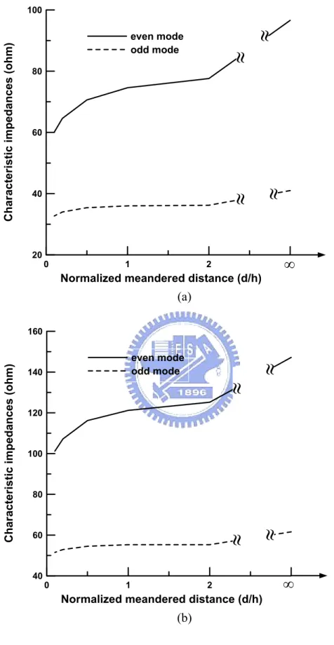
parallel-coupled line are different from those of the conventional parallel-coupled line. Figure 3.3 shows the variations of Z0e and Z0o of a meandered parallel-coupled line
with different meandered distance. The curves shown in Figure 3.3 (a) corresponds to a meandered parallel-coupled line with w=20 mils, s=10 mils, L=600mils (capital L represents the total line length), and 50mil-thick Rogers RT6010 (εr=10.2) substrate.
From Figure 3.3 (a), it can be observed that the Z0e drastically reduces as the
meandered distance decreases. And Z0o just reduces a little. In order to see detail, we
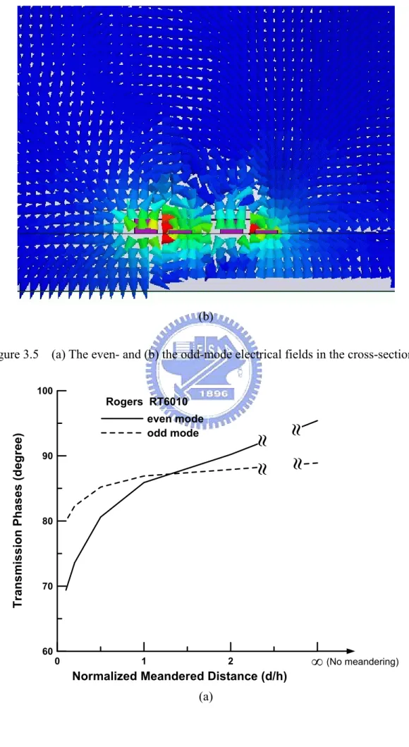
use 3D-Electroamagnetic (EM) simulator, High Frequency Structure Simulator (HFSS), to analysis the 3D structure that is shown in Figure 3.4. Figure 3.5 (a) points out that as the two coupled lines are excited in even mode, there are strong fields in the meandering region. That makes the total even-mode capacitance Ce drastically
increases, and according to equation (2.7a), Z0e reduces drastically. On the other hand,
Figure 3.5 (b) indicates as the two coupled lines are excited in odd mode, there are still some weak fields in the meandering region, but the field strength is not as strong as the fields between the two main coupled lines. Therefore, odd-mode capacitance Co
only slightly increases, and Z0o reduces slightly. In addition, characteristics of a
meandered parallel-coupled line with a 20mil-thick Rogers RO4003 (εr=3.38)
substrate, and physical parameter of w=10, s=4, and L=980 mils is shown in Figure 3.3 (b). The behaviors are similar to that of Figure 3.3 (a).
The θe and θo of the meandered parallel-coupled line are also different to those of
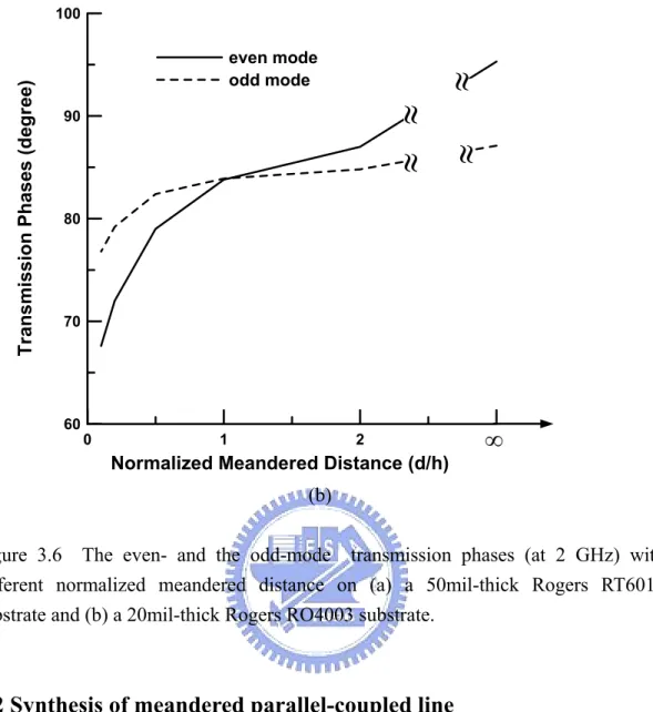
the conventional parallel-coupled line. Figure 3.6 (a) and (b) depict the θe and θo of
the meandered parallel-coupled lines with identical physical parameters as Figure 3.3 (a) and (b). Figure 3.6 indicates that the θe drastically reduces as d decreases.
However, θo just has a little reduction. The main reason is the field distribution of the
meandered parallel-coupled line is the similar to that of Schiffman section as the coupled line is excited by even mode. Therefore, the meandering induces dispersive effect and effectively speeds the Vep up. On the other hand, however, the field
distribution of the odd-mode excitation is not similar to Schiffman, so there is no obvious speeding-up effect for Vop.
0 1 2 3
Normalized meandered distance (d/h)
20 40 60 80 100 Cha rac te ristic i m pe da nces (ohm) even mode odd mode
∞
≈
≈
≈
≈
(a) 0 1 2 3Normalized meandered distance (d/h)
40 60 80 100 120 140 160 Cha racte ristic i m pedances (ohm) even mode odd mode
∞
≈
≈
≈
≈
(b)Figure 3.3 The even- and the odd-mode characteristic impedances with different normalized meandered distance on (a) a 50mil-thick Rogers RT6010 substrate and (b) a 20mil-thick Rogers RO4003 substrate.
Figure 3.4 A standard meandered parallel coupled line in HFSS.
(b)
Figure 3.5 (a) The even- and (b) the odd-mode electrical fields in the cross-section.
0 1 2 3
Normalized Meandered Distance (d/h)
60 70 80 90 100 T ra n s m iss io n Ph as es (d eg ree ) even mode odd mode Rogers RT6010 (No meandering)
∞
≈
≈
≈
≈
(a)0 1 2 3
Normalized Meandered Distance (d/h)
60 70 80 90 100 T ra n sm is si on P h as es ( d eg ree ) even mode odd mode
∞
≈
≈
≈
≈
(b)Figure 3.6 The even- and the odd-mode transmission phases (at 2 GHz) with different normalized meandered distance on (a) a 50mil-thick Rogers RT6010 substrate and (b) a 20mil-thick Rogers RO4003 substrate.
3.2 Synthesis of meandered parallel-coupled line
We hope that we can proper synthesis the physical dimensions of the meandered parallel-coupled line for various applications. However, there are no exact analysis or synthesis equations for meandered parallel-coupled line so that the circuit simulator such as Agilent ADS or AWR Microwave office is needed to analyze the behaviors of meandered parallel-coupled line. This section will describe how to use the circuit simulator to synthesize the exact physical dimensions of meandered parallel-coupled line according to the desired electrical parameters.
A standard meandered parallel-coupled line is shown in Figure 3.1, which comprises an interconnecting coupled line, a coupled-Schiffman section, and two coupled-line corners. The interconnecting coupled line uses the standard microstrip coupled line model in circuit simulator. The coupled-Schiffman section and the coupled-line corners are modeled in most of circuit simulators based on look up table of EM results. Using circuit simulator can quickly extract optimal dimensions of w, s,
l, and d in Figure 3.1. These dimensions have different weightings for coupler’s modal
characteristic impedances and modal transmission phases. In order to obtain desired coupling, the goal of the even- and the odd-mode characteristic impedance should be properly chosen respectively. Because the dimensions of w and s have larger weightings than l and d for the modal characteristic impedances of coupler, we optimize w and s in circuit simulator to obtain the desired modal characteristic impedances at desired frequency. Return loss is the criteria to observe whether the modal characteristic impedances to be fitted or not. On the other hand, in order to make the center frequency to locate at desired frequency, θ =90o (the average of modal transmission phases) is the criteria at desired center frequency. θe and θo should
be equal at certain frequency where we want to get a good isolation. The dimensions d and l have larger weightings than w and s for the modal transmission phases of meandered section. The desired modal transmission phases can be obtained by adjusting d and l. However, because the modal characteristic impedances and modal transmission phases affect each other during adjusting process, iteration process is needed. We use the physical dimensions of conventional microstrip parallel coupler with the desired electrical parameters to be the initial guess in optimized procedures. Empirically, after several iteration cycles, the exact physical dimensions of meandered parallel-coupled line with desired electrical parameters can be obtained.
3.3 Coupler with ultra high directivity within a narrow band
According to the description in section 3.1, the coupled Schiffman section, a main part of meandered parallel-coupled line, can equivalently speed up the even-mode phase velocity. The scheme can be used to produce an intersection of θe
and θo at any frequency point, and get an ultra high directivity at that frequency. This
section will design a 10-dB coupler with ultra high directivity at 2.4 GHz based on single-section meandered parallel-coupled line, as shown in Figure 3.1, and fabricate it on an 50mil-thick Rogers RT6010 substrate with dielectric constant of 10.2.
From the specifications described above, the proper electrical parameters are Z0e
=69.4 ohm and Z0o =36 ohm respectively. The physical dimensions of the coupler can
be obtained initially by a circuit simulator. Both the weightings of physical dimensions for various electrical parameters and the iteration procedures are described in detail in section 3.2. Once obtaining these physical dimensions form the circuit simulator, the EM simulator such as Sonnet is used to do the fine tuning for getting the optimum performance. Finally, the optimum value of w=27 mils, s=12 mils, l=189 mils, d=30 mils is obtained by EM simulator. The modal transmission phases are shown in Figure 3.7. It can be found in Figure 3.7 that the even- and the
odd-mode transmission phases intersect at 2.4 GHz where the desired center frequency locates. The simulated and measured return losses are shown in Figure 3.8. Since a single-section meandered parallel-coupled line has an asymmetric layout between input and coupled port, the return loss data are took from the two ports. The simulated and measured return loss data agree well, and all show better than 20 dB return loss up to 2.6 GHz.
Figure 3.9 shows the simulated and measured coupling responses. We can observe the simulated and measured couplings are -12.4 dB and -12.3 dB at 2.4 GHz, respectively. The curves are matched well.
The simulated and measured isolations are -76 and -67 dB at center frequency, respectively, as shown in Figure 3.10. The measured response matches well with the simulated one, and both have a more than 40 dB improvement comparing to that of conventional coupler.
Figure 3.11 shows the simulated and measured directivities. The simulated and measured directivities are 64.6 and 54.7 dB at center frequency, respectively, and they match well around center frequency. Figure 3.12 (a) and (b) show the layout and photograph of proposed coupler.
Figure 3.7 The modal transmission phases of single section meandered parallel-coupled line.
1.2 1.6 2 2.4 2.8 3.2 3.6 Frequency (GHz) -60 -40 -20 0 R e tr un Lo ss (d B) simulated-input measured-input simulated-coupled measured-coupled
Figure 3.8 The simulated and measured return losses of the single section meandered parallel-coupled line.
1.2 1.6 2 2.4 2.8 3.2 3.6 Frequency (GHz) -40 -35 -30 -25 -20 -15 -10 -5 0 Co upling (dB) simulated measured
Figure 3.9 The simulated and measured couplings of the single section meandered parallel-coupled line.
1.2 1.6 2 2.4 2.8 3.2 3.6 Frequency (GHz) -80 -60 -40 -20 0 Isolation (dB) simulated measured
Figure 3.10 The simulated and measured isolations of the single section meandered parallel-coupled line. 1.2 1.6 2 2.4 2.8 3.2 3.6 Frequency (GHz) -20 0 20 40 60 80 Dir ec tivity (dB) simulated measured
Figure 3.11 The simulated and measured directivities of the single section meandered parallel-coupled line.
From these results, we give some conclusions. First, it can be observed that the return losses in Figure 3.8 drastically get worse when the frequency is higher than 3 GHz. The reason is that the Z0e of single section meandered parallel-coupled line
varies as frequency when the frequency is higher than about 1.5 times of center frequency. Figure 3.13 (a) shows a simplified equivalent circuit of Figure 3.1. Here, the coupled-line corner and interconnect coupled line are absorbed into coupled Schiffman section. The various dimensions of this single section meandered parallel-coupled line are shown in Figure 3.13 (a). With even mode excitation, Figure 3.13 (a) can be simplified to Figure 3.13 (b), a meandered single microstrip line with 2w+s of line width. The electrical parameters are Z0e =48.8 ohm, Z0o =32.8 ohm, εer_eff
=7.88, and εor_eff =6.07 for the circuit in Figure 3.13 (b). Refer to [24], the image
impedance Zi of the structure shown in Figure 3.13 (b) is the square root of Z0e by Z0o.
Therefore, if we set the port impedance to be the theoretical Zi, 40 ohm, we should get
a perfect port matching. But it isn’t correct for our case. Because the theory of [24] is based on TEM mode, however, the εe
r_eff, and εor_eff in the structure of Figure 3.13 (b)
are not equal. Thus, it is not a pure TEM mode. The obtained return losses shown in Figure 3.14 (a) are not a perfect port matching. And the return losses are worse than -20 dB as the frequency is higher than 2.5 GHz. Here, we tune the Zi to be 34.7 ohm
to obtain a wider port matching bandwidth. The results are shown in Figure 3.14 (b). It indicates the return losses are better than -20 dB as the frequency is lower than 3.5 GHz. We can get the desired Zi by this way. Since Zi is equivalent to the shunt circuit
of the two coupled lines with characteristic impedance Z0e, the Z0e is two times of Zi,
69.4 ohm, the value that we want. This value is useful when frequency is lower than 3.5 GHz. When frequency is higher than 3.5 GHz, the Z0e still drastically varies as
frequency due to the inherent characteristic of the meandered coupled line. Fortunately, the Z0o of single section meandered parallel-coupled line is almost a
constant of frequency, just likes the Z0o in conventional parallel coupler. Therefore,
the main reason that makes the return loss of the proposed coupler to get worse is the non-constant characteristic of Z0e.
Second, since the proposed structure in Figure 3.1 is an asymmetric structure, mode coupling would be happen. That means the even and odd mode will simultaneously exist whether even or odd mode is excited. In this case, the even- and odd-mode scattering parameters can be calculated from the normal-mode scattering parameters obtained by EM simulation and then the mode coupling can be observed. The magnitude of the mode coupling can be as high as one-third that of excitation mode (about -10dB of mode conversion). Fortunately, the analysis based on even- and odd-mode analysis is still useful and it will be proved by several design examples.
In addition, the right-angle corner in Figure 3.1 would produce radiation loss or surface wave loss. As shown in Figure 3.15, the sum of square of normal scattering parameters is less than unity as frequency goes high. That implies the radiation loss or surface wave loss exists and results in extra loss.
Finally, Figure 3.2(b) indicates that the θe versus frequency will be a curve due
to the dispersion (or speeding-up) effect. And we know that the θo versus frequency is
almost linear for a meandered parallel-coupled line. It is known that every phase versus frequency curve of a quasi-TEM coupled line started from the origin of the coordinate. Unfortunately, a curved line like Figure 3.2(b) and a linear straight line can only have one intersection point other than zero frequency. There is only one intersection at center frequency as shown in Figure 3.7. This means that this coupler can only have one ultra-high directivity frequency point where it is chosen to be the certain frequency.
(a)
(b)
Figure 3.12 The (a) layout and (b) photograph of the coupler with ultra high directivity.
w=27
s=12
d=30
l=270
(a)w=27+12+27
d=30
l=270
Zi
(b)Figure 3.13 (a) The simplified equivalent circuit of Figure 3.1 (b) the simplified equivalent of (a) in even mode excitation. (Unit: mils)
0 2 4 6 8 10 Frequency (GHz) -60 -40 -20 0 Po rt Mat chin g R etu rn Loss (dB )
model in Figure 3.13 (a) model in Figure 3.13 (b) -180 -90 0 90 180 Tr an sm is sio n P ha se ( deg re e ) (a) 0 2 4 6 8 10 Frequency (GHz) -80 -60 -40 -20 0 Po rt M a tc h ing R etu rn Loss (dB)
model in Figure 3.13 (a) model in Figure 3.13 (b) -180 -90 0 90 180 Tr an sm is si on Phas e (de g ree) (b)
Figure 3.14 The port matching responses and transmission phases of the equivalent circuits in Figure 3.13 with (a) theoretical Zi and (b) tuned Zi..
0 1 2 3 4 5 Frequency (GHz) 0.9 0.92 0.94 0.96 0.98 1 T h e s u m of sq ua re of sc at te ring p a ramet er s
Figure 3.15 The sum of square of scattering parameters versus frequency.
3.4 Coupler with high directivity over broad bandwidth
Last section described the single-section meandered parallel-coupled line can only get ultra-high directivity around a narrow frequency band. In order to make the high directivity bandwidth wider like a pure TEM coupled line, we propose a multisection meandered parallel coupler, as shown in Figure 3.16(a). Cascading of several identical unit-meandered-sections forms the proposed coupler. The unit-meandered-section is shown in Figure 3.16(b). Figure 3.17 shows the transmission phase of conventional and proposed coupler. Here, we pay our attention to the bandwidth between 0 and 2fo, which is the main operation bandwidth of a
coupler. In Figure 3.17, the modal transmission phases of conventional parallel-coupled-line coupler are shown as solid lines. In addition, in order to explain conveniently, we neglect the tiny variation of the odd-mode transmission phase caused by meandering. The even-mode transmission phases of whole coupler with one, two and five meandered sections are shown in Figure 3.17. In Figure 3.17, the θe
with one meandered section is a curve, and as the number of the meandered section increases, the even-mode transmission phase approaches a straight line. The
dispersion curve of θe approaches a straight line because only a small portion of θe
curve is taken as the number of section increases. Therefore, θe can approach θo over a
very wide bandwidth. Based on the scheme, a microstrip coupler with nearly ideal TEM coupler performance can be achieved over the entire coupler bandwidth.
Input Coupled Isolated Through unit meandered section 1 N 2 (a) w s d
Interconnecting coupled line
l Coupled Schiffma n section Coupled-line corner Coupled-line corner (b)
Figure 3.16 (a) The multisection meandered parallel-coupled line. (b) The unit-meandered-section.
Because an ideal TEM coupler repeats its response every 2fo, the target of the
design is to equalize θe and θo within 2fo (i.e. within the first period of response). We
take a 20-dB coupler at 1GHz as a design example. The circuit is fabricated on an 8mil-thick Rogers RO4003 substrate with dielectric constant of 3.38. In order to