array using the patch-antenna coupler formed by placing one or two open-ended microstrip lines (coupled lines) near and along the nonradiating edge(s) of a patch antenna. An -band five-element array with broadside 25-dB Chebyshev radiation is demonstrated. When the input signal is fed to the center element, with most of the power radiating from the antenna, part of it is tapped to the coupled lines, amplified by an FET amplifier, and fed to the next antenna element. This process is repeated after all the antenna elements are fed with suitable power. The amplitude distribution of the fields radiated from the antennas is controlled by the coupling coefficient from the patch to the coupled line, which, in turn, is governed by the coupling length and gap between the patch and line. The measured return loss of the designed five-element array is 27 dB at the center frequency of 10 GHz with 2% 10-dB bandwidth. The radiation pattern possesses a transmitting gain of 15.9 dB, a half-power beamwidth of 17 , and a sidelobe level of 22 dB.
Index Terms—Active antenna, amplifying array, patch-antenna coupler, spatial power combining.
I. INTRODUCTION
A
LTHOUGH the patch antenna has gained in popularity since the 1970s, the improvement of its inherent narrow bandwidth has been a very active area for research. Parasitic el-ement(s) (i.e., transmission line(s) with open ends on both sides) along the nonradiating edge(s) of a patch antenna was used to improve the match to 50 and to increase the patch impedance bandwidth [1], [2]. Later, the coupled parasitic element (one end open, but the other end used as a connecting port) was used as a feedback network to integrate an FET oscillator with the patch antenna [3], [4]. A simple equivalent distributed circuit was shown in [3] to present that most of energy is conserved in-side the patch.Particularly compatible with modern monolithic integrated circuit (MIC) technology, solid-state devices have been used to
Manuscript received May 11, 2001. This work was supported by the Ministry of Education and by the National Science Council, R.O.C., under Contract 89-E-FAO6-2-4.
C.-H. Tsai was with the Department of Communication Engineering, National Chiao Tung University, Hsinchu, Taiwan, R.O.C. He is now with the Darfon Electronics Corporation, Tainan, Taiwan, R.O.C.
Y. A. Yang is with Trimble Navigation System, Sunnyvale, CA 94088-3642 USA.
S.-J. Chung is with the Department of Communication Engineering, National Chiao Tung University, Hsinchu, Taiwan, R.O.C. (e-mail: [email protected]).
K. Chang is with the Department of Electrical Engineering, Texas A&M University, College Station, TX 77843 USA.
Publisher Item Identifier 10.1109/TMTT.2002.801335.
(a)
(b)
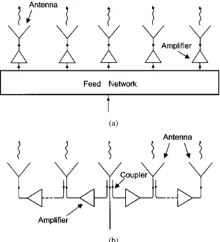
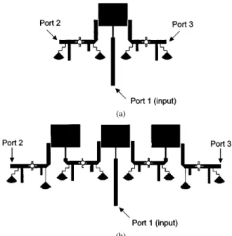
Fig. 1. Diagrams of: (a) a conventional amplifying array and (b) the proposed amplifying array.
combine several component functions at the terminals of the patch antenna. The integrated antennas can reduce the size, weight, and cost of many transmitting and receiving systems. These active integrated antennas are ideal for spatial and quasi-optical power combining [5]–[9].
Among the various configurations of the integrated antennas, the circuit-fed amplifying antenna arrays [6]–[9], which are formed by implementing amplifiers in the antenna array, are constructed for high-power and high-gain applications. In these arrays, the input power is distributed to each antenna element through a parallel or series feed network. A solid-state amplifier is embedded at the front of each antenna element to amplify the power distributed to the element. Fig. 1(a) shows the diagram of such an amplifying array. Although the concept is simple and straightforward, there are a number of drawbacks for this configuration. One is that the biasing of the amplifiers is inconvenient to design since all the amplifiers are dc con-nected. Another is that lots of the power dividers with different power-split ratios need to be implemented to construct the feed network. This consumes much of the circuit area, increases the size and design complexity, especially for a large antenna array. This paper presents the design and measurement of a new amplifying antenna array using a novel concept proposed by the 0018-9480/02$17.00 © 2002 IEEE
Fig. 2. Circuit layout of a five-element amplifying array using patch-antenna couplers.
authors in [10]. As shown in Fig. 1(b), the array is composed of antenna elements, couplers, and amplifiers. When the power is fed to the center element through the array input port, with most of it radiated by that antenna element, part of the power is tapped out by the coupler(s) to the nearby transmission line(s). The coupled power is amplified by an FET amplifier and then fed to the next antenna element. The process is repeated after all the antenna elements are fed with suitable power. Based on this new excitation technique, a 10-GHz five-element patch-antenna array, as shown in Fig. 2, is demonstrated. To make the structure compact, the function performed by the antenna element and coupler is fulfilled by using a patch antenna with a coupled open-ended microstrip line (hereafter referred to as the patch-antenna coupler). The patch-antenna coupler can be viewed as an asymmetric coupled transmission line. By simply adjusting the coupling length and/or the gap between the patch and open-ended line, different levels of coupling energy can be controlled so as to generate a beam-shaped array with proper excitation amplitude distribution (Chebyshev, uniform, or binomial). No bulky power-divider feed network is needed. On the other hand, tuning the lengths of the microstrip lines connecting the adjacent antennas could control the phase distribution. It is noted that the gap between the patch and coupled transmission line also serves as a dc block for the biasing of the FET amplifier, which greatly simplifies the bias circuit in the active array.
This paper is organized as follows. Section II presents the simulated and measured characteristics of the patch-antenna coupler. The coupling coefficient as functions of both the coupling length and gap are studied. Based on the results, a five-element amplifying antenna array, as shown in Fig. 2, is designed and described in Section III. The array is designed to have a broadside 25-dB Chebyshev amplitude distribution. To this end, a fixed-gain FET amplifier is first designed and measured carefully to obtain the designed gain level and phase. The coupling coefficient for each patch-antenna coupler is then calculated to fulfill the array amplitude distribution. To simplify the design, the required coupling coefficients are accomplished by only varying the coupling length of the patch-antenna coupler. Section IV presents the measurement results, including the return loss and radiation pattern of the fabricated amplifying array. The results of the array with some
(b)
Fig. 3. Configurations of the patch-antenna couplers with: (a) a coupled line and (b) dual coupled lines.
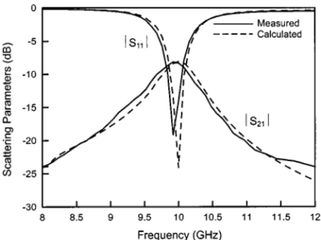
Fig. 4. Measured and calculated frequency responses of the return loss(S ) and coupling coefficient(S ) of the patch-antenna coupler with a coupled line. L 2 W = 9:6 212 mm , l = 0:8L, g = 0:3 mm.
amplifiers off are also shown and compared. Discussions and conclusions are followed in Sections V and VI, respectively.
II. ANALYSIS OFPATCH-ANTENNACOUPLERS
The five-element amplifying array is built on a 20-mil (0.508-mm) RT/Duroid 5880 ( ) substrate. Two types of antenna couplers are needed in this array, one with a coupled line [see Fig. 3(a)] and the other with dual coupled lines [see Fig. 3(b)]. The coupled lines are placed along the patch’s nonradiating edges with a gap and a coupling length . A 50- microstrip line of width ( mm) is used to feed the antenna through a quarter-wave transformer. The coupled lines are also 50- lines with width of . The full-wave electromagnetic (EM) simulator IE3D using the method of moment (Zeland Software Inc., Fremont, CA) is adopted for
(a)
(b)
Fig. 5. (a)H- and (b) E-plane measured radiation patterns of the patch antennas with a coupled line (l = 0:8L, g = 0:3 mm) and without coupled line.L 2 W = 9:6 212 mm , f = 10 GHz.
simulation. For an operating frequency at 10 GHz, the designed length and width of the patch antenna without coupled lines are 9.6 and 12 mm, respectively. This patch size is fixed in the following analysis. Although placing the coupled line(s) beside the patch would influence the resonant condition and thus change the antenna’s resonant frequency, the effect is small (since the coupling is weak) and can be easily compensated by fine tuning the length and width of the quarter-wave transformer.
The frequency responses and radiation patterns are first inves-tigated. Fig. 4 illustrates the measured and designed frequency responses of the return loss and coupling coefficient of a patch-antenna coupler [see Fig. 3(a)] with and
0.3 mm. The measured return-loss response is quite the same as an ordinary patch antenna, which shows a resonant frequency at 9.92 GHz (only 0.8% off the designed one) and a 10-dB bandwidth of 2.2%. The coupling coefficient first in-creases and then dein-creases as the frequency is raised, with a maximum of 8.17 dB around the resonant frequency. Note that the experimental results agree very well with the calculated ones. The radiation patterns of the patch could be deteriorated due to the presence of the coupled line. To see how much the coupled line would affect the patterns, a separate patch antenna without the coupled line is made and measured. Fig. 5(a) and (b) compares the measured - and -plane radiation patterns of these two antennas. When measuring the patch-antenna coupler, the coupled port is terminated with a 50- resistor. As shown,
(a)
(b)
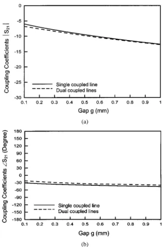
Fig. 6. (a) Amplitude and (b) phase as functions of the coupling gapg of the calculated coupling coefficientsS of the patch-antenna couplers shown in Fig. 3.L 2 W = 9:6 212 mm , l = 0:8L, f = 10 GHz.
the antenna with a coupled line has a 3-dB -plane beamwidth of about 70 and -plane beamwidth of 85 . The antenna gain at broadside is 6.34 dBi, which is a little lower than that of the antenna without the coupled line. This gain reduction may be due to the power coupling effect. The cross-polarization levels of the two antennas are 20 dB lower than the co-polarization levels at a broadside direction. In particular, the antenna cou-pler has similar, if not lower, cross-polarization levels as does the ordinary patch antenna. Generally speaking, the coupled line exhibits little influence on the radiation patterns.
The purpose of designing the patch-antenna coupler is to con-trol power coupling from the patch to the coupled line. Different levels of power coupling can be achieved by varying the cou-pling length and gap of the coupled line. As a function of the gap, Fig. 6 depicts the variations of the calculated cou-pling coefficient (amplitude and phase) at 10 GHz for the two configurations shown in Fig. 3. The coupling length is fixed at . Note that, for the antenna coupler with dual coupled lines [see Fig. 3(b)], the coupling coefficient to port 3 is the same as that to port 2 due to the symmetry of the struc-ture. Evidently, a smaller gap would result in a higher coupling [see Fig. 6(a)]. The amplitude of the coupling coefficient could reach 6 dB when the gap is as narrow as 0.1 mm. Also, the coupling is about the same no matter if one or two coupled lines are used. The difference between the coupling coefficients of the two configurations can only be distinguished when the gap be-comes narrower (higher coupling). Finally, it is noticed that the
(a)
(b)
Fig. 7. (a) Amplitude and (b) phase as functions of the normalized coupling lengthl =L of the calculated and measured coupling coefficients S of the patch-antenna couplers shown in Fig. 3.L2W = 9:6212 mm , g = 0:3 mm, f = 10 GHz.
phase of the coupling coefficient [see Fig. 6(b)] changes very limited when the gap is varied.
As a function of the coupling length , Fig. 7 presents the calculated variations of the coupling for the two configu-rations. For verification, the measured results obtained using the transmission-reflection-line (TRL) calibration technique [11] for the antenna coupler with a coupled line is also shown. The gap is fixed at 0.3 mm. As observed from Fig. 7(a), the coupling level first raises with the increase of the coupling length. A maximum level of about 7.9 dB is reached when . Further increase of the length causes a slight decrease of the coupling. Unlike the coupling level, the phase of the coupling coefficient shown in Fig. 7(b) reduces monoton-ically with the increase of the coupling length. This variation of the phase is more pronounced as compared to that for the change of the gap [see Fig. 6(b)]. Notice that the experimental results are in good agreement with the calculated ones.
Before leaving this section, it is noted that, for each case of different coupling length or gap shown above, the antenna’s input return loss is always controlled under 20 dB at 10 GHz by tuning the length and width of the quarter-wave transformer.
III. DESIGN OF THEAMPLIFYINGANTENNAARRAY A linear five-element amplifying array, as shown in Fig. 2, is designed. The inter-element spacing of this -plane array is
(a)
(b)
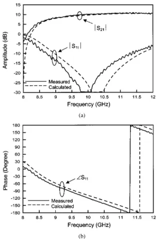
Fig. 8. (a) Amplitude response of the transducer gain(S ) and input return loss(S ). (b) Phase response of the transducer gain (S ) of the FET amplifier. V = 2 V, I = 20 mA.
set as 21 mm, which corresponds to 0.7 free-space wavelength. The array is designed to have a Chebyshev broadside radia-tion pattern with a sidelobe level of 25 dB. The five patch antennas are symmetrically located with respect to the center one, where the external power is fed in. Four amplifiers are needed to implement the array. For simplicity, these amplifiers are with the same design and, thus, have equal gain and trans-mission phase delay. The excitation voltages to generate the Chebyshev pattern are controlled by the coupling lengths of the patch-antenna couplers. Only two types of antenna couplers are required, i.e., a dual-coupled-lines antenna (the center element) and a single-coupled-line antenna (the ones next to the center element).
A. Design of the FET Amplifier
The amplifier is designed with the device NE32584c (a pseu-domorphic heterojunction FET). Based on the scattering pa-rameters of the transistor measured from the TRL calibration technique, the matching network is obtained [12] utilizing the commercial software HP Series IV (Hewlett-Packard Inc., Santa Rosa, CA). Fig. 8(a) and (b) illustrates the amplitude response and phase response, respectively, of the transducer gain and input return loss at the bias condition of V and mA. Both the measurement and simulation results are presented, which show good agreement with each other. The measured gain has a level of 10 dB at 10 GHz with approx-imately 0.5-dB gain flatness from 9.6 to 10.6 GHz. The return
Fig. 9. Design diagram for the five-element Chebyshev amplifying array.
loss at the center frequency is better than 30 dB. The measured phase delay with additional 1-mm extensions at both the input and output ports is 108.4 . The phase delay of the amplifier plays an important role in the design of the broadside array.
B. Design of the Coupled Lines and Feed Lines
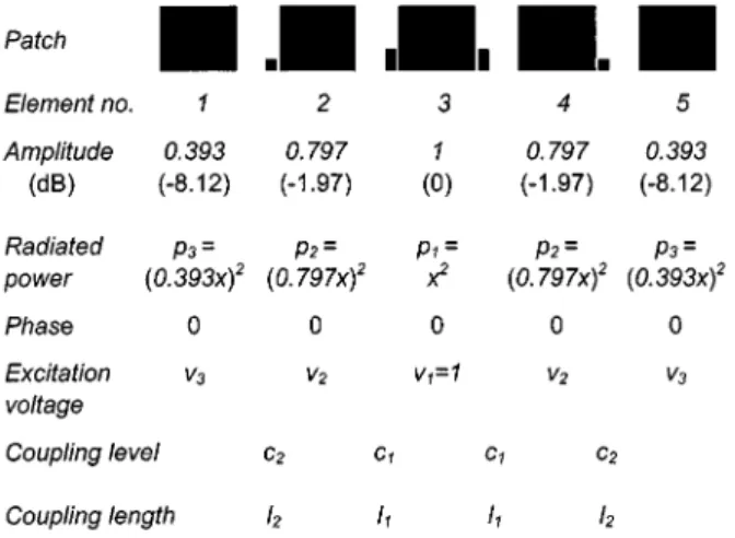
Fig. 9 illustrates a design diagram for the five-element ampli-fying array. The normalized amplitude distribution for a 25-dB Chebyshev array is, from elements 1–5, 0.393 ( 8.12 dB), 0.797 ( 1.97 dB), 1 (0 dB), 0.797 ( 1.97 dB), and 0.393 ( 8.12 dB) [13]. These values correspond to those practically radiated from the antennas. Let the power radiated from the center element (element 3) be . The power radiated from elements 2 and 4 and that from elements 1 and
5 are, thus, and , respectively. To meet
this power distribution requirement, the coupling lengths (element 3) and (elements 2 and 4) should be adjusted to obtain suitable coupling levels and , respectively. The normalized excitation voltage applied to the center element is denoted as ( ), as for elements 2 and 4, and as for elements 1 and 5.
The power radiated from the center element is the difference between the excitation power and the power coupled to both sides of the coupled lines (neglecting the power loss due to other effects), i.e.,
(1) or
(2) Similarly, the power radiated via element 2 or 4 is the difference between the excitation power and the power coupled to the transmission line or
(3) where the excitation power for element 2 or 4 is the power coupled from the center element (with coupling level ) and amplified by the amplifier (with gain )
(4)
By substituting (5), (4), and (2) into (6) with , the power radiated from the center element can be calculated
as dB. The required coupling
levels and are then solved, using (2) and (5), to be 0.0575 ( 12.4 dB) and 0.023 ( 16.38 dB), respectively. These coupling levels can be achieved by choosing proper coupling lengths while keeping a fixed gap. (For the ease of fabrication, the gap is set at 0.3 mm in this study.) The measured results shown in Fig. 7(a) suggest that the required coupling length of the center element is 2.55 mm and that of elements 2 or 4 is 1.65 mm.
For broadside radiation, the signal phases at the feed points of all the patch antennas should be the same. This is accomplished by designing the lengths of the feed lines connecting adjacent antennas so that the signal phase delay be equal to a multiple of 360 . As observed from Fig. 2, the phase delay includes those of the antenna coupler, FET amplifier, quarter-wave transformer, and two extra sections of microstrip lines (before and after the amplifier). The phase delays via the first three components are fixed from the above design, while that of the extra microstrip lines can be tuned to meet the phase requirement by adjusting their lengths.
In order to verify the designed coupling lengths and feed-line lengths, two separate circuits, as shown in Fig. 10 (which are parts of the final amplifying array), are made and measured. The one-stage circuit in Fig. 10(a) contains a patch antenna with one-stage coupling and amplifying, and the two-stage cir-cuit in Fig. 10(b) is composed of three patch antennas with two-stage coupling and amplifying. All the FET amplifiers in each configuration have the same bias ( V and
mA). During measuring, port 3 of each circuit is connected to a 50- resistor for termination. Fig. 11(a) and (b) shows the measured scattering parameters. Both the circuits have a 10-dB return-loss bandwidth of 2% centered at the de-sign frequency (10 GHz) with return loss of 25 dB. For the one-stage circuit, the measured transmission loss illus-trated in Fig. 11(a) is 2.2 dB at the center frequency, which is only 0.2 dB lower than the desired value (2.4 dB). The measured transmission phase delay , after incorporating the effect of the extended input feed line, corresponds to a phase differ-ence of 7.8 between the feed points of the center element and element 2 (or 4) in the final array. Although a zero phase differ-ence is needed, this measured value is still under the tolerance of fabrication and measurement. From Fig. 11(b), the measured transmission loss for the two-stage circuit at 10 GHz is 8.2 dB, which, again, is very close to the design one (8.64 dB). Also, from the measured phase delay , the corresponding
(b)
Fig. 10. Circuit layouts of the: (a) one-stage circuit and (b) two-stage circuit.
(a)
(b)
Fig. 11. Measured scattering parameters for the: (a) one-stage circuit and (b) two-stage circuit shown in Fig. 10.V = 2 V, I = 20 mA.
phase difference between the feed points of the center element and element 1 (or 5) is 4.3 . In general, the experimental results are in good agreement with the design ones.
IV. MEASUREMENT OF THEAMPLIFYINGANTENNAARRAY The five-element amplifying array is fabricated after the step-by-step design process described above. The return loss
Fig. 12. Measured return loss of the fabricated five-element amplifying array. V = 2 V, I = 20 mA.
Fig. 13. MeasuredH-plane radiation patterns of the fabricated five-element amplifying array.V = 2 V, I = 20 mA, f = 10 GHz.
and radiation patterns with and without the amplifiers on are measured. Fig. 12 depicts the measurement result for the return loss. The array exhibits a resonant frequency at 10 GHz, with a return loss of 27 dB. The 10-dB return-loss bandwidth is 2%, the same as those of the one- and two-stage circuits presented in the previous section. Actually, since the coupling used in the array is weak, the return loss depends mainly on the input matching of the center element, with little influence from other circuits and antennas.
The radiation patterns of the antenna array are measured using an -band standard horn antenna with a gain of 15.8 dBi at 10 GHz. This receiving horn is placed at a distance of 190 cm, which is in the far-field zone of the array. Since the linear array is formed along the -plane of the antenna element, only the -plane patterns are measured. The resultant co- and cross-polarization patterns are shown in Fig. 13. It is seen that the array possesses a 3-dB beamwidth of 17 and a gain of 15.9 dBi. From the design data shown in Fig. 9, the theoretical gain of the array should be 17 dB, which is
10.6 dB higher
than the gain (6.4 dBi) of a single patch antenna. Thus, the experimental gain is only 1.1 dB lower than the theoretical one, corresponding to a power combining efficiency of about 90%. Also observed from the co-polarization pattern, the measured
(a)
(b)
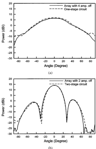
Fig. 14. MeasuredH-plane radiation patterns of the: (a) one-stage circuit and amplifying array with all the amplifiers off and (b) two-stage circuit and amplifying array with the two side amplifiers off.V = 2 V, I = 20 mA, f = 10 GHz.
sidelobe level is 22 dB lower than the peak value, which is close to the expected one (25 dB). The cross-polarization level is about the same as the sidelobe level of the co-polarization pattern, but with a deep null at the broadside direction.
In the applications of the amplifying antenna array, it is im-portant to study the graceful degradation of the array perfor-mance. To investigate the effect of the damaged devices on the radiation pattern, the array with some amplifiers off (by turning off their bias voltages) is measured. Fig. 14(a) shows the mea-sured radiation pattern of the amplifying array with all ampli-fiers off. That of the one-stage circuit shown in Fig. 10(a) is also presented for comparison. As expected, the patterns of these two configurations are similar and are much broader than that of the array with amplifying since now only one patch antenna effec-tively radiates in the array. Fig. 14(b) shows the measured radia-tion patterns of the two-stage circuit [see Fig. 10(b)] and the am-plifying array with only the middle two amplifiers on. The an-tenna gain and 3-dB beamwidth of the partially damaged array are 14.1 dBi and 27 , respectively, which are, again, similar to those of the two-stage circuit. As compared to the normal ampli-fying array, the gain of the present case decreases and the beam is broadened since the two edge antennas are nonradiating.
V. DISCUSSIONS
It is interesting to compare the transmitting gains of the pro-posed amplifying antenna array and the conventional one.
Re-the EIRP of Re-the proposed amplifying array [see Fig. 1(b)] is expressed as
(8) Here, the reduction of the antenna gain due to the coupling ef-fect of the coupled lines has been neglected. It is seen that the array gain ratio between the proposed array and conventional one is . This ratio is less than unity for a small array, but would be greater than one when a large array is formed. Also, it is noticed from Fig. 1 that amplifiers are used in the conventional array, while only amplifiers are in the pro-posed array. If an additional amplifier is put at the input of the proposed array, the EIRP in (8) should be modified as
(9) As compared to (7), the proposed amplifying array has an EIRP or, equivalently, a transmitting gain times that of the conven-tional one.
VI. CONCLUSIONS
An amplifying antenna array employing the patch-antenna coupler has been proposed and demonstrated with a five-ele-ment array with broadside 25-dB Chebyshev amplitude distri-bution. The radiation pattern of the array can be shaped by de-signing the coupling factors of the antenna couplers, which, in turn, are achieved by controlling the coupling length and gap. The design of the amplifying array, including that of the ampli-fier and antenna couplers, is based on a step-by-step process. At most steps, both simulation and experimental approaches have been used to confirm the design. The measured results for the fabricated five-element array agree quite well with the expected ones. The measured transmitting gain, half-power beamwidth, and sidelobe level are 15.9 dBi, 17 , and 22 dB, respectively. It is also found that the input return loss of the array depends es-sentially only on the matching of the patch antenna to be exter-nally fed, not influenced by other circuits or antennas. As com-pared to the conventional amplifying array, the proposed array leads to significant advantages such as compactness of the con-figuration, ease of biasing, and high transmitting power.
REFERENCES
[1] J. R. Mosig and F. E. Gardiol, “The effect of parasitic elements on mi-crostrip antennas,” in IEEE AP-S Int. Symp. Dig., 1985, pp. 397–400.
[7] R. A. York and Z. B. Popovic´, Eds., Active and Quasi-Optical Arrays
for Solid-State Power Combining. New York: Wiley, 1997.
[8] A. Mortazawi, T. Itoh, and J. Harvey, Eds., Active Antennas and
Quasi-Optical Arrays. Piscataway, NJ: IEEE Press, 1998.
[9] M. Belaid, J.-J. Laurin, and K. Wu, “Integrated active antenna array using unidirectional dielectric radiators,” IEEE Trans. Microwave
Theory Tech., vol. 48, pp. 1628–1634, Oct. 2000.
[10] Y.-C. Yang, S.-J. Chung, and K. Chang, “Novel active antenna ampli-fying arrays,” in IEEE MTT-S Int. Microwave Symp. Dig., 1998, pp. 997–1000.
[11] D. M. Pozar, Microwave Engineering. New York: Wiley, 1998. [12] G. Gonzalez, Microwave Transistor Amplifiers Analysis and
De-sign. Englewood Cliffs, NJ: Prentice-Hall, 1997.
[13] C. A. Balanis, Antenna Theory Analysis and Design. New York: Wiley, 1997.
Chih-Hung Tsai was born in Kaohsiung, Taiwan,
R.O.C., in 1974. He received the B.S. degree in elec-tronic engineering from the National Taipei Univer-sity of Technology, Taipei, Taiwan, R.O.C., in 1996, and the M.S. degree in communication engineering from the National Chiao Tung University, Hsin-chu, Taiwan, R.O.C., in 2000.
He is currently engaged in development of a low-temperature co-fired ceramic (LTCC) module at the Darfon Electronics Corporation, Tainan, Taiwan, R.O.C.
Yaochou A. Yang (S’97–M’97) was born in Tainan,
Taiwan, R.O.C., in 1968. He received the B.S.E.E. and M.S.E.E. degrees from Texas A&M University, College Station, in 1995 and 1997, respectively.
In July 2000, he joined Trimble Navigation System, Sunnyvale, CA, where he has been involved in the global positioning system (GPS) receiver’s system and circuit development. His technical interests include nonlinear microwave circuits, active antennas, RF integrated circuits (RFICs), and signal integrity.
Kai Chang (S’75–M’76–SM’85–F’91) received the
B.S.E.E. degree from the National Taiwan Univer-sity, Taipei, Taiwan, R.O.C., in 1970, the M.S. de-gree from the State University of New York at Stony Brook, in 1972, and the Ph.D. degree from The Uni-versity of Michigan at Ann Arbor, in 1976.
From 1972 to 1976, he was with the Microwave Solid-State Circuits Group, Cooley Electronics Laboratory, The University of Michigan at Ann Arbor, where he was a Research Assistant. From 1976 to 1978, he was with Shared Applications Inc., Ann Arbor, MI, where he was involved with computer simulation of microwave circuits and microwave tubes. From 1978 to 1981, he was with the Electron Dynamics Division, Hughes Aircraft Company, Torrance, CA, where he was involved in the research and development of millimeter-wave solid-state devices and circuits, power combiners, oscillators, and transmitters. From 1981 to 1985, he was with TRW Electronics and Defense, Redondo Beach, CA, where he was a Section Head involved with the development of state-of-the-art millimeter-wave integrated circuits and subsystems, including mixers, voltage-controlled oscillators (VCOs), transmitters, amplifiers, modulators, upconverters, switches, multipliers, receivers, and transceivers. In August 1985, he joined the Electrical Engineering Department, Texas A&M University, College Station, as an Associate Professor, and became a Professor in 1988. In January 1990, he became an E-Systems Endowed Professor of Electrical Engineering. He has authored and co-authored several books, including Microwave Solid-State Circuits and Applications (New York: Wiley, 1994), Microwave Ring Circuits and Antennas (New York: Wiley, 1996), Integrated Active Antennas and Spatial Power Combining (New York: Wiley, 1996), and RF and Microwave Wireless Systems (New York: Wiley, 2000). He has served as the Editor of the four-volume Handbook of Microwave
and Optical Components (New York: Wiley, 1989 and 1990). He is the Editor
of Microwave and Optical Technology Letters and the Wiley Book Series on “Microwave and Optical Engineering.” He has also authored or co-authored over 350 technical papers and several book chapters in the areas of microwave and millimeter-wave devices, circuits, and antennas. His current interests are in microwave and millimeter-wave devices and circuits, microwave integrated circuits, integrated antennas, wide-band and active antennas, phased arrays, microwave power transmission, and microwave optical interactions.
Dr. Chang was the recipient of the 1984 Special Achievement Award pre-sented by TRW, the 1988 Halliburton Professor Award, the 1989 Distinguished Teaching Award, the 1992 Distinguished Research Award, and the 1996 Texas Engineering Experiment Station (TEES) Fellow Award presented by Texas A&M University.