Quantitative Analysis of a Flat-Top Planar
Waveguide Demultiplexer
Chun-Ting Lin, Student Member, IEEE, Yang-Tung Huang, Member, IEEE, and Jung-Yaw Huang
Abstract—A three-focal-point method is used for the design of a flat-top planar waveguide concave grating. With the Gaussian approximation a modified formula is proposed and is compared with the numerical model of the scalar diffraction theory by using a design example. The sources of loss caused by the flat-top design and the grating are taken into consideration. The optimal separa-tion between the two outmost focal points is obtained and the spec-tral response of the demultiplexer with a ripple below 0.04 dB is achieved.
Index Terms—Concave grating, flat-top, planar waveguide, three-focal-point method, wavelength-division multiplexing.
I. INTRODUCTION
N
OWADAYS, the increasing demand for optical band-widths in the optical telecommunication network is driven by the explosive growth of Internet. Wavelength di-vision multiplexering (WDM) systems use each wavelength as a separate channel. With the progress of the laser and the opto-electronic device, it is possible to have a high density of wavelengths in a single fiber and it is known as dense wave-length division multiplexing (DWDM). DWDM increases the transmission capacity of a fiber by increasing the wavelength channel numbers rather than increasing the data bit rate. There-fore, the performance of the optical network depends greatly on the spectral characteristics of the components it uses, such as the crosstalk, the passband width, and the insertion loss.Planar waveguide demultiplexers/multiplexers, such as arrayed waveguide gratings (AWGs) and planar waveguide concave (etched) gratings, are of recent interest for wave-length-division-multiplexed fiber communication systems because of their low insertion loss, low crosstalk, high possibil-ities of mass production, and high spectral resolution. With the progress of semiconductor process, the sizes of the electronic or optical devices become smaller and smaller. Monolithic integration of the electronic and optical components may
Manuscript received March 27, 2008; revised June 18, 2008. Current version published April 17, 2009. This work was supported by the National Science Council of China under Contract NSC96-2221-E-009-111.
C.-T. Lin and J.-Y. Huang are with the Department of Photonics and Insti-tute of Electro-Optical Engineering, National Chiao Tung University, Hsinchu 30010, Taiwan (e-mail: rhino.eo91g@nctu.edu.tw; jyhuang@faculty.nctu.edu. tw).
Y.-T. Huang is with the Department of Electronics Engineering and Insti-tute of Electronics, and the Department of Biological Science and Technology, National Chiao Tung University, Hsinchu 30010, Taiwan (e-mail: huangyt@cc. nctu.edu.tw).
Color versions of one or more of the figures in this paper are available online at http://ieeexplore.ieee.org.
Digital Object Identifier 10.1109/JLT.2008.2004932
be feasible in the future. In many cases, arrayed waveguide gratings face the problems of larger device sizes and extreme fabrication tolerances required for higher channel numbers and narrower channel spacing [1]. In contrast, the sizes of planar waveguide concave gratings can be much smaller than that of AWGs by five times in the equivalent applications [2]. However, a conventional planar waveguide demultiplexer gives a sharp spectral response and is temperature sensitive due to the temperature dependence of refractive indexes of waveguide materials, which limits the applications in the WDM system. Many techniques [3]–[12] have been proposed to overcome the problem by flattening the spectral response of the devices.
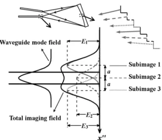
In this paper, a three-focal-point method, which was proposed for a flat-top planar waveguide demultiplexer [6], is used to ob-tain the flat-top spectral response. With a Gaussian approxima-tion, the formula derived form the reference paper is modified to obtain the optimal half-separation when the spot size of each Gaussian subimaging field is different from that for the output waveguide mode field. The grating is divided into three inter-leaved subgratings with different focal points and each focal point lies on the cross-sectional line of the ending facet for the output waveguide. Each subgrating forms subimage with ap-proximately the same spot size and each subimage overlaps with each other.
To obtain a flattened spectral response, the central subimage focuses on the center of the ending facet for the output wave-guide and the two outmost subimages are separated from each other with the distance of . For a symmetric spectral response, the peak amplitudes of the field for the two outmost subimages are designed to be identical. With the Gaussian field approxima-tion, the value of the half-separation determines the optimal ratio of the peak amplitude for the central subimage and the out-most subimage according to the modified formula. Moreover, a numerical model of the scalar diffraction theory [13] is intro-duced and used to verify the modified formula with a numerical example. The sources of loss and dispersion characteristics are considered in the numerical calculation.
II. MODIFIEDFORMULABASED ONGAUSSIANAPPROXIMATION
In this paper, the grating is composed of three interleaved subgratings with different focal points and each focal point lies on the cross-sectional line of the ending facet for the output waveguide as shown in Fig. 1 [6]. Each subimage formed by the corresponding subgrating overlaps with each other. With the Gaussian field approximation, the total field distribution with
where , , and denote the peak amplitudes of the three subimages, respectively, denotes the half-separation between the two outmost subimages, denotes the spatial dispersion coefficient of the grating along the -axis, denotes the fre-quency of the light, denotes the central frequency, and denotes the spot size of each Gaussian subimage (the spot sizes for three subimages are approximately the same since the sub-gratings are interleaved [6]). To obtain a symmetric spectral re-sponse, and are designed to be identical. The effective half widths of the input and output waveguides for the funda-mental modes are and , respectively. The spec-tral response of one channel can be obtained from the following overlap integral over the whole cross section of the ending facet for the output waveguide [6]
(2) where denotes the Gaussian mode field distribu-tion of the output waveguide and has the form
(3)
After the operation of convolution, the spectral response can be expressed as
(4)
To obtain a flat spectral response, the curvature of the spectral response in (2) at the central frequency should be zero, and
can be obtained as
(5) This equation shows that the ratio is a function of the half-separation when the spot size of each subimage and the effective half width of the output mode field are determined.
Fig. 1. Schematic figure for the three-focal-point method based on the Gaussian approximation.
III. DESIGNEXAMPLE ANDNUMERICALANALYSIS
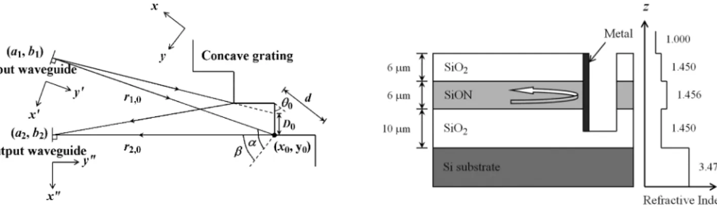
In this section, a planar waveguide concave grating based on the recursive definition of facet positions is introduced [13] and it was first proposed by McGreer in 1996. Simulation results show that a concave grating of the classical Rowland circle de-sign suffers from the spherical aberration more seriously than that for the recursive-definition design [14]. The recursive-def-inition design is more potential and predominate than other de-signs. One least constraint function must be first defined. The free-aberration position of each groove is determined by the so-lution of the root for this constraint function, i.e., [13]
(6) where denotes the location of the vertex for the th groove, denotes the distance between and as shown in Fig. 2, denotes the diffraction order, denotes the design wavelength, and denotes the effective index of the wave propagated in the slab waveguide. The tilt angle of the th facet with respect to the axis is determined by the fol-lowing equation [13]:
(7) Light launched form the input waveguide is diffracted by the grating, focused to the position along the imaging curve, and guided into different output waveguides according to the corresponding wavelengths. The focal equation of the concave grating has the following form [15]:
(8) where and denote the incident angle and the diffraction angle of the input Gaussian beam at the grating pole, respec-tively, is the effective radius of the grating. The numerical model of the scalar diffraction theory for the concave grating in
Fig. 2. Schematic figure of the light propagated in the slab waveguide and dif-fracted by the concave grating.
Fig. 3. Cross-sectional views of the input and output channel waveguides.
the planar waveguide was first proposed in 1995 [16], and the field formula is used in our analysis
(9) where denotes the effective facet width of the th grating facet, denotes the effective half width of the input wave-guide, denotes the angle between the ending facet normal for the input waveguide and light divergence to the th grating facet, denotes the half angle for the Gaussian beam divergence at amplitude, denotes the propagation constant in the slab waveguide, and de-note the incident angle and the diffraction angle with respect to the th grating facet normal, respectively.
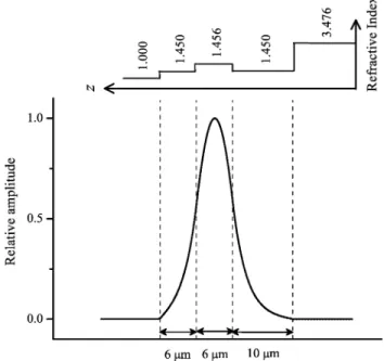
A design example of the concave grating in silica-on-silicon is used to illustrate the three-focal-point method. The input and output channel waveguides consist of the SiON core layer with a m cross-sectional area surrounded by the SiO cladding layer as shown in Fig. 3. The slab waveguide consists of a 6- m-thick SiON core layer with the upper 6- m-thick and lower 10- m-thick SiO cladding layers as shown in Fig. 4. The grating is achieved by etching a trench to the lower cladding layer and then coated with metal at the back wall. Therefore, light is reflected, diffracted, and focused by the metalized con-cave grating.
Fig. 4. Side view of the slab waveguide.
The following parameters are chosen: for the refractive index of the core layer, for the re-fractive index of the cladding layer, for the refrac-tive index of the silicon substrate at an operating wavelength of 1550.12 nm, the effective numerical aperture NA of 0.13 for the input waveguide which is the same as that for the commercial single-mode fiber, 81 channels in the C-band with the channel
spacing nm (50 GHz) from 1528.77 nm to
1560.61 nm according to ITU grids [17], for the in-cident angle at the grating pole, the diffraction order , m for the period of the grating facet blazed at an angle obtained form (7), for the total number of periods, m for the distances form the end of the input waveguide and the end of the design output waveguide to the grating pole, and m for the effective ra-dius of the grating. By using the transfer-matrix method [18], the effective indexes of the TE and TM modes are obtained as 1.45393 and 1.45392, respectively. The propagation losses due to the leakages to the silicon substrate for both modes are less than 0.03 dB/cm when the thickness of the lower cladding layer is higher than 10 m.
The E-field distribution for the TE mode within the slab waveguide in Fig. 4 is shown in Fig. 5. The effective half widths, and , of the input and output waveguides for the fundamental modes along the axis and the axis are 4.91 m obtained with BeamPROP software from R-Soft and the half angle for the beam divergence can be obtained as 3.96 . The spot size of each subimage along the
axis is 5.85 m . The spectral response
of each channel can be obtained from the overlap integral over the whole cross section of the ending facet for the output waveguide
(10) where denotes the loss attributed to the grating or the wave-guide including the undesired-order loss and the propagation loss. Here, the fiber coupling loss is not considered. The unde-sired-order loss, which comes form the diffraction of light into undesired adjacent orders, is one of the main sources of loss.
To make a comparison between the modified formula de-rived in (5) and the numerical modeling of the scalar diffraction theory for the three-focal-point method, we take the TE mode
Fig. 5. E-field distribution for the TE mode within the slab waveguide as shown in Fig. 4.
for example. All computer program codes for the simulation are written in Fortran 90. If the subgratings are interleaved, the ratio of the peak amplitudes of the subimages is approximately equal to the ratio of the facet numbers of the corresponding sub-gratings [6]. So we can adjust the ratio of the facet numbers of subgrating 2 and subgrating 1 to adjust the ratio . If the grating pole is located at the origin of the coordinates, after de-termining the arrayed sequence of the facets of the subgratings the axis coordinate position of the vertex of the th groove can be obtained as
(11) where denotes the grating period of subgrating , denotes the diffraction order, denotes the central wavelength of sub-grating , denotes the effective index in the slab waveguide, denotes the incident angle at the grating pole, and denotes the diffraction angle at the grating pole. The order for each subgrating is identical but with the different grating period and central wavelength to obtain a flat-top spectral response. Then the axis coordinate position can be obtained from the solu-tion of the root for (6). This multigrating method in which each subgrating has its own path-length increment and central wave-length has also been used in the AWG device design [4].
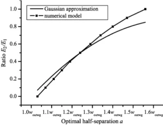
The optimal half-separation can be obtained when the spec-tral response with a minimum ripple is achieved. The ripple is defined as the maximum difference among three extremum points within 3-dB passband of one channel. Fig. 6 shows the ratio as a function of for the cases of the Gaussian ap-proximation and our numerical model where the axis is cali-brated in . It shows that the deviation between the two curves becomes serious as the ratio is close to unity and the two curves have the same value of 0.7 when the optimal half-separation is . For the case of the Gaussian approximation, only the amplitude term of the
Fig. 6. E =E versus the optimal half-separation a as w = 1:19w .
imaging field is taken into consideration as shown in (1). For the case of our numerical model, both the amplitude and phase terms of the imaging field are taken into consideration as shown in (9). So there exists the difference between the two curves for the cases of the Gaussian approximation and the numerical model as shown in Fig. 6. Without considering the scattering loss and side-wall tilt loss at the grating facet, the spectral re-sponses of the central channel for the two cases as
, , and are shown in
Fig. 7. The spatial dispersion coefficient in our case is . The insertion loss for the case of our numer-ical model is 4.40 dB, where 2.19 dB comes from the excess loss for the flat-top design and 2.21 dB comes from the loss in (10) which is predominated by the undesired-order term. The
1-dB passband width for the case of the Gaussian approxi-mation is larger than that for the case of our numerical model due to no phase term of the imaging field being taken into con-sideration. As mentioned in Section II, for a symmetric spec-tral response the peak amplitudes and are designed to be identical with identical facet numbers. However, and are slightly different due to the different effective widths of adja-cent facets and therefore it increases the ripple in the spectral response.
The total field distribution of the image and the field profile of the output fundamental mode at the ending facet of the output waveguide are shown in Fig. 8. To obtain a flat-top spectral response, the imaging field distribution is just like camelback. For the case of our numerical model, the 1-dB passband width and the crosstalk versus the ratio with the channel spacing of 50 GHz for the central channel are shown in Fig. 9. It shows that the 1-dB passband width increases as the ratio increases, while the decreased (better) crosstalk is obtained. The optimal half-separation is obtained with a minimum ripple, and the ripple is below 0.04 dB which is shown in Fig. 10. The excess loss, the coupling loss from the slab wave-guide to the output channel wavewave-guide, versus the ratio is shown in Fig. 11. Fig. 12 shows the spectral responses of the central five channels with and without the flat-top designs for the undesired-order loss of 2.21 dB. It is shown that the flattened spectral responses can be obtained but the insertion loss will be
Fig. 7. Flattened spectral responses of the central channel for the two cases of the Gaussian approximation and the numerical model asE =E = 0:7, a = 1:52w , andw = 1:19w .
Fig. 8. Total field distributionE of the image and the field profileE of the output fundamental mode at the ending facet of the output waveguide.
sacrificed. The above simulation results show that the passband width for the flat-top design can be changed by changing the ratio , which then determines the optimal half-separation as shown in Fig. 6. More numerical examples in Figs. 13 and 14 show that the value of the intersection point of the two curves decreases as the spot size of the subimage decreases and the in-tersection point falls on a point with a ratio of 0.5 and an
optimal half-separation of as .
At the intersection point, the optimal half-separation obtained from (5) has the same value with that obtained from the com-puter simulation by using our numerical model. When changes as changes for the assigned values of and in (5), the intersection points of the two curves in Figs. 13 and 14 also change as changes due to the different changes of for the two cases.
The chromatic dispersion characteristic is expressed as [6]
(12)
Fig. 9. 01-dB passband width and the crosstalk versus the ratio E =E with the channel spacing of 50 GHz for the central channel as w = 1:19w .
Fig. 10. Ripple versus the ratioE =E as w = 1:19w .
Fig. 11. Excess loss versus the ratioE =E as w = 1:19w .
where is the group delay given by [6]
(13) and where is the velocity of the light in vacuum, and is the phase response obtained from the overlap integral
Fig. 12. Flattened spectral responses of the central five channels with and without the flat-top design for the channel spacing of 50 GHz as w = 1:19w .
Fig. 13. E =E versus the optimal half-separation a as w = w .
. The chromatic dispersion characteristics are shown in Fig. 15 for the cases with and without the flat-top designs. It shows that the flat-top design has the better chromatic dispersion characteristic than that without the flat-top design. The chromatic dispersion characteristic for the case of the flat-top design ranges from 12.35 to 8.91 ps/nm within the 1-dB passband width. The flat-top design has the flatter spectral response within the passband resulting in the slowly-changing phase response so it has the better chromatic dispersion characteristic.
IV. CONCLUSION
In this paper, a modified formula for the three-focal-point method is proposed and compared with a numerical model of the scalar diffraction theory by a design example. Simulation results show that the deviation between the two cases becomes serious
Fig. 14. E =E versus the optimal half-separation a as w = 0:88w .
Fig. 15. Spectral responses and the chromatic dispersion characteristics with and without the flat-top design asw = 1:19w .
as the ratio approaches unity and the optimal half-sepa-ration can be approximately obtained using the modified for-mula. The changed passband width can be achieved by changing the ratio . The chromatic dispersion characteristic is also considered in this paper. It is feasible to achieve the flat-top planar waveguide concave grating using the three-focal-point method.
ACKNOWLEDGMENT
The authors would like to thank H.-H. Lin at Industrial Tech-nology Research Institute, Hsinchu, Taiwan, for the simulation discussions and the continuous encouragement.
REFERENCES
[1] K. Takada, M. Ade, T. Shibita, and K. Okamoto, “A 25-GHz-spaced 1080-channel tandem multi/demultiplexer covering the S-, C-, and L-bands using an arrayed-waveguide grating with Gaussian passbands as primary filter,” IEEE Photon. Technol. Lett., vol. 14, no. 5, pp. 648–650, May 2002.
[2] S. Janz, A. Balakrishnan, S. Charbonneau, P. Cheben, M. Cloutier, A. Delâge, K. Dossou, L. Erickson, M. Gao, P. A. Krug, B. Lamontagne, M. Packirisamy, M. Pearson, and D.-X. Xu, “Planar waveguide echelle gratings in silica-on-silicon,” IEEE Photon. Technol. Lett., vol. 16, no. 2, pp. 503–505, Feb. 2004.
[3] M. R. Amersfoort, J. B. D. Soole, H. P. LeBlanc, N. C. Andreadakis, A. Rajhel, and C. Caneau, “Passband broadening of integrated arrayed waveguide filters using multimode interference couplers,” Electron. Lett., vol. 32, no. 5, pp. 449–451, Feb. 1996.
[4] A. Rigny, A. Bruno, and H. Sik, “Multigrating method for flattened spectral response wavelength multi/demultiplexer,” Electron. Lett., vol. 33, no. 20, pp. 1701–1702, Sep. 1997.
[5] C. Dragone, “Efficient techniques for widening the passband of a wave-length router,” J. Lightw. Technol., vol. 16, no. 10, pp. 1895–1906, Oct. 1998.
[6] Z. Shi and S. He, “A three-focal-point method for the optimal design of a flat-top planar waveguide demultiplexer,” IEEE J. Sel. Top. Quantum Electron., vol. 8, no. 6, pp. 1179–1185, Nov./Dec. 2002.
[7] J.-J. He, “Phase-dithered waveguide grating with flat passband and sharp transitions,” IEEE J. Sel. Top. Quantum Electron., vol. 8, no. 6, pp. 1186–1193, Nov./Dec. 2002.
[8] C. R. Doerr, L. W. Stulz, and R. Pafchek, “Compact and low-loss in-tegrated box-like passband multiplexer,” IEEE Photon. Technol. Lett., vol. 15, no. 7, pp. 918–920, Jul. 2003.
[9] J. Song, D. Pang, and S. He, “A planar waveguide demultiplexer with a flat passband, sharp transitions and a low chromatic dispersion,” Opt. Commum., vol. 227, pp. 89–97, 2003.
[10] Z. Shi, J.-J. He, and S. He, “An analytic method for designing passband flattened DWDM demultiplexers using spatial phase modulation,” J. Lightwave Technol., vol. 21, no. 10, pp. 2314–2321, Oct. 2003. [11] X. Chen, J. N. McMullin, C. J. Haugen, and R. G. DeCorby, “Planar
concave grating demultiplexer for coarse WDM based on confocal el-lipses,” Opt. Commum., vol. 237, pp. 71–77, 2004.
[12] C. Dragone, “Low-loss wavelength routers for WDM optical networks and high-capacity IP routers,” J. Lightw. Technol., vol. 23, no. 1, pp. 66–79, Jan. 2005.
[13] K. A. McGreer, “Theory of concave gratings based on a recursive def-inition of facet positions,” Appl. Opt., vol. 35, no. 30, pp. 5904–5910, Oct. 1996.
[14] C.-T. Lin, Y.-T. Huang, J.-Y. Huang, and H.-H. Lin, “Integrated planar waveguide concave gratings for high density WDM systems,” in Proc. Opt. Commun. Syst. Netw., Banff, AB, Canada, Jul. 19–21, 2005, pp. 98–102.
[15] M. C. Hutley, Diffraction Gratings. London, U.K.: Academic, 1982, p. 228.
[16] K. A. McGreer, “Diffraction from concave gratings in planar waveg-uides,” IEEE Photon. Technol. Lett., vol. 7, no. 3, pp. 324–326, Mar. 1995.
[17] S. V. Kartalopoulos, Introduction to DWDM Technology. New York: IEEE Press, 2000, p. 184.
[18] H. Kogelnik, “Theory of optical waveguides,” in Guided-Wave Opto-electronics, T. Tamir, Ed. Berlin, Germany: Springer-Verlag, 1990, ch. 2.
Chun-Ting Lin (S’05) was born in Taipei, Taiwan,
in 1977. He received the B.S. and M.S. degrees in electrophysics from National Chiao Tung University, Hsinchu, Taiwan, in 2000 and 2002, respectively, where he is currently working toward the Ph.D. degree in electro-optical engineering.
His current research is focused on integrated op-tical devices for opop-tical communication systems.
Yang-Tung Huang (M’90) was born in Taiwan, in
1955. He received the B.S. degree in electrophysics and the M.S. degree in electronics from National Chiao Tung University, Taiwan, in 1978 and 1982 respectively, and the Ph.D. degree in electrical and computer engineering (minor in optical sciences) from the University of Arizona, Tuscon, in 1990.
He is a Professor at the Department of Electronics Engineering and the Institute of Electronics, and a Joint Professor at the Department of Biological Sci-ence and Technology, National Chiao Tung Univer-sity, Taiwan. He has been the Director of Institute of Electronics for three years, the Director of Semiconductor Research Center for two years, and the Director of Nano Facility Center for four years. His current researches include inte-grated optics, photonic crystal waveguides, bio-optoelectronics, and optoelec-tronic switching networks.
Dr. Huang received the Outstanding Research Award from the National Sci-ence Council in 1998.
Jung-Yaw Huang received the Ph.D. from Applied
Physics Department, Cornell University Ithaca, NY, in 1988.
Currently he is a Full Professor of Department of Photonics and Institute of Electro-Optical Engi-neering at National Chiao Tung University, Hsinchu, Taiwan. His research interests focus on the devel-opment of various optical probes for characterizing surface and bulk properties of frontier functional materials at the femtosecond and nanometer scales.