應用於單晶片多處理器系統之任務結合方法
56
0
0
全文
(2) 應用於單晶片多處理器系統之任務結合方法 Task Binding on Multi-Processor System-on-Chip. Student: Chen-Ling Chou. 研 究 生:周志杰. Advisor: Dr. Jing-Yang Jou. 指導教授:周景揚 博士. 國立交通大學 電子工程學系 電子研究所碩士班 碩士論文. A Thesis Submitted to Department of Electronics Engineering & Institute of Electronics College of Electrical Engineering and Computer Science National Chiao Tung University in Partial Fulfillment of the Requirements for the Degree of MASTER OF SCIENCE in Electronics Engineering. July 2004 Hsinchu, Taiwan, Republic of China. 中 華 民 國 九 十 三 年 七 月.
(3) 應用於單晶片多處理器系統之任務結合方法. 研究生:周志杰. 指導教授:周景揚. 博士. 國 立 交 通 大 學 電 子 工 程 學 系. 電 子 研 究 所 碩 士 班. 摘要. 採用單晶片網路為通訊架構來建立以矽智財元件為基礎之系統 單晶片是一種新的設計方法。這種設計方法的特性是具有高度的可重 複使用性以及延展性。在這篇論文裡,我們詳述一個二步驟的任務結 合演算法。利用這個演算法所建立的工具可將一個以參數化任務圖所 描述的應用結合至以二維網狀交換器為通訊骨幹之單晶片多處理器 系統平台上。該演算法嘗試將任務結合至可使用的計算資源上並且使 得整個應用的運算時間降到最小以及將系統效能提升至最大。結合軟 體處理器以及交換器模型之後,我們可以模擬整個系統。在短時間之 內,我們可以檢視系統的效能並且萃取重要的平台參數。. i.
(4) Task Binding on Multi-Processor System-on-Chip Student: Chieh-Chieh Chou. Advisor: Dr. Jing-Yang Jou. Department of Electronics Engineering Institute of Electronics National Chiao Tung University. Abstract Network-on-Chip is a new design paradigm for designing core based System-on-Chip. It features high degree of reusability and scalability. In this thesis, we describe a two-step task binding algorithm that has been used to build a tool to map an application, described by a parameterized task graph, onto Multi-Processor System-on-Chip platform with a two dimensional mesh of switches as a communication backbone. The algorithm tries to find a mapping of tasks to available computational resources so that the overall execution time of the application is minimized and the system performance gain is maximized. By incorporating software processor and switch models, a system simulation can be performed. And in few minutes, the system performance gain can be assessed and some important platform parameters can be extracted.. ii.
(5) Acknowledgment First and foremost, I would like to express my sincere gratitude to my advisor Professor Jing-Yang Jou for his suggestions and guidance throughout the years. As my advisor, he not only helped me on my work, but also gave me a lot of valuable advice on my life. I was such a lucky guy to have worked with him. Also, I would like to thank Cheng-Yeh Wang, Liang-Yu Lin, and Pao-Jui Huang; they were the first people I would go to whenever I needed support or to share my happiness and sorrow. Without their help, I wouldn’t have finished my work and learned so much. Special thanks to EDA lab and VSP lab members, for their company and friendship; it has been a great time to be together with them. Finally, I would like to express my sincere gratitude to my family and all my friends, who have always helped and encouraged me a lot.. iii.
(6) Contents 摘要.................................................................................................................................i Abstract ..........................................................................................................................ii Acknowledgment ......................................................................................................... iii Contents ........................................................................................................................iv List of Figures ...............................................................................................................vi List of Tables.............................................................................................................. viii Chapter 1 Introduction ...................................................................................................1 1.1 A Design Paradigm Shift..................................................................................1 1.2 Related Works ..................................................................................................2 1.3 Thesis Organization .........................................................................................3 Chapter 2 Preliminary ....................................................................................................4 2.1 Our Platform ....................................................................................................4 2.2 Switch Design ..................................................................................................5 2.2.1 Switching Strategies..............................................................................5 2.2.2 Features of Our Switch .........................................................................8 2.2.3 Switch Model ......................................................................................12 2.3 Our Design Flow............................................................................................14 Chapter 3 Task Binding................................................................................................17 3.1 Problem Formulation .....................................................................................17 3.2 Task Binding Flow .........................................................................................18 3.3 Task Mapping.................................................................................................19 3.3.1 Simulated Annealing...........................................................................20 iv.
(7) 3.3.2 Cost Function ......................................................................................22 3.3.3 Annealing Schedule ............................................................................23 3.4 Connection Path Assignment .........................................................................24 3.4.1 Pathfinder Algorithm ..........................................................................24 3.4.2 Routing Resource Graph.....................................................................26 3.4.3 Cost Function ......................................................................................29 Chapter 4 Experimental Results...................................................................................32 4.1 Experiment Flow............................................................................................32 4.2 Experimental Results .....................................................................................34 4.2.1 Routability Analysis............................................................................34 4.2.2 Performance Analysis .........................................................................35 4.2.3 Scalability Analysis.............................................................................37 Chapter 5 Conclusion and Future Work.......................................................................40 Reference .....................................................................................................................42 VITA ............................................................................................................................46. v.
(8) List of Figures Figure 1 Our platform ....................................................................................................4 Figure 2 Deadlock..........................................................................................................8 Figure 3 Two unidirectional virtual channels multiplexed across a physical channel...9 Figure 4 Messages make progress rather than being blocked......................................10 Figure 5 Virtual channels sharing the bandwidth of a physical channel using round-robin schedule ...................................................................................................10 Figure 6 Virtual channels sharing the bandwidth of a physical channel using weighted round-robin schedule ...................................................................................................11 Figure 7 Inside the switch ............................................................................................12 Figure 8 Processor 1 sending two works to processor 2..............................................14 Figure 9 Our design flow .............................................................................................15 Figure 10 Task binding flow ........................................................................................19 Figure 11 Local versus global optima..........................................................................21 Figure 12 Pseudo-code for generic simulated annealing placer ..................................22 Figure 13 A bounding box............................................................................................23 Figure 14 Pseudo-code for Pathfinder algorithm.........................................................25 Figure 15 Routing resource graph for a processor and its local switch .......................27 Figure 16 Routing resource graph for a switch............................................................28 Figure 17 Routing resource graph across a physical channel ......................................29 Figure 18 Our experiment flow....................................................................................32 Figure 19 Mapping between output of each case and its corresponding task graph....33 Figure 20 A task with two inputs and three outputs.....................................................34 vi.
(9) Figure 21 Requirement of channel width factor over 765 cases..................................35 Figure 22 Performance measurement ..........................................................................36 Figure 23 Relationship between communication load and processor utilization rate .37 Figure 24 Experiment with the maximum number of inputs or outputs equal to 4 .....38 Figure 25 Experiment with the maximum number of inputs or outputs equal to 7 .....39. vii.
(10) List of Tables Table 1 Comparison of different switching strategies ...................................................7 Table 2 Base cost for each type of routing resource ....................................................30. viii.
(11) Chapter 1 Introduction. 1.1 A Design Paradigm Shift As silicon technology scales, people today are able to integrate billions of transistors on a chip. However, as more and more components are integrated, several problems emerge. First of all, shared-bus based system does not work well. Usually, buses can efficiently handle 3 to 10 communication partners, but they do not scale to higher numbers [1][2][3]. Secondly, since technology scaling works better for transistors than for interconnecting wires, wire delay is no longer negligible. It’s hard to maintain global synchrony, for long and global wires make system performance unpredictable [1][3][4]. Thirdly, each component in a complex system is usually developed by different teams at different times with different design languages and tools. At system level, these components are not easily composable because a tiny change in one part may have unexpected effects on other seemingly unrelated parts of the system [1]. Consequently, more design efforts are spent on verification, which in turn lowers the design productivity and delays product development. Recently, Networks-on-Chip design methodology is proposed to solve these problems. A typical NoC architecture provides a scalable communication infrastructure for interconnected components; and Globally Asynchronous Locally Synchronous (GALS) style of large chip implementation is supported. Each component could be implemented as a separate clock domain and could communicate 1.
(12) to other components using asynchronous communication through switches. By managing communication channels properly, data transmission can coexist peacefully. This allows arbitrary components to be integrated and connected to a network, while adding new resources to a bus-based system has great impact on system performance [5][6][7]. Also, each component can be designed and verified independently because each one is guaranteed to comply with the network protocol standard. By reusing pre-designed and pre-verified components, a new system can be quickly built-up and much verification effort can be saved.. 1.2 Related Works There are many research works in this field. [8][9][10][11] propose integrated modeling, simulation and implementation environment. In [8], NoC infrastructure and processors are modeled, and then simulation is performed to find the optimal network configuration. [9] and [10] try to refine the network communication protocol and a protocol controller is synthesized in [10]. [11] tries to model multiprocessor and real-time operating system to analyze the behavior of a complex system that has real-time applications running on a multiprocessor platform. Design issues of the NoC architecture, including switch design, network topology and protocol, are discussed in [7][12][13]. [12] proposes a data-transfer method called Black-Bus, which saves up to 75% of routing tags compared to the global addressing scheme used in traditional packet network. [7] exploits circuit switching technique to guarantee communication bandwidth. [13] proposes a communication protocol stack that can guarantee traffic bandwidth. In both [7] and [13], 2D-mesh is chosen as the network topology. [14] proposes a two-step genetic algorithm that has been used to build a tool for 2.
(13) binding an application, described by a parameterized task graph, onto NoC architecture with a two dimensional mesh of switches as a communication backbone. To calculate the execution time of the system, a NoC architecture specific communication delay model is presented. The algorithm tries to bind tasks onto processors so that the overall execution time of the application is minimized. In our work, we try another way to bind tasks onto processors for two reasons. First, connection paths between each pair of interconnected tasks are pre-allocated in our platform, which is not in [14]. Second, a task graph will be manipulated before tasks are mapped onto processors. Therefore, no scheduling will be performed in the binding process.. 1.3 Thesis Organization The rest of the thesis is organized as follows. Chapter 2 introduces our Multi-Processor System-on-Chip (MPSoC) platform, the switch design considerations, the model of this switch and our design flow. In Chapter 3, details about task binding techniques we use are presented. Then, experiment flow and experimental results are given and discussed in Chapter 4. Finally, the conclusion is made in Chapter 5.. 3.
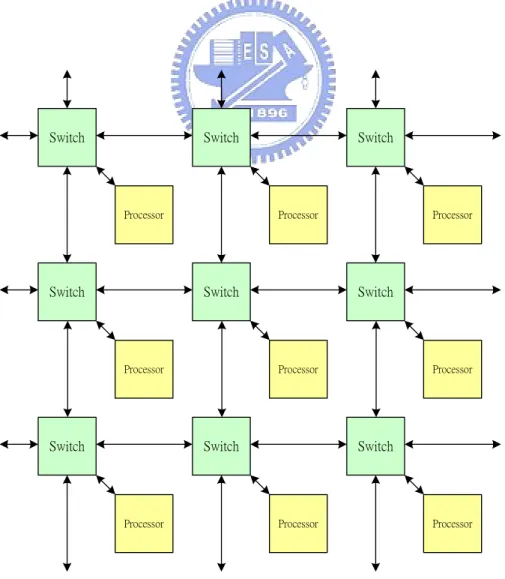
(14) Chapter 2 Preliminary. 2.1 Our Platform As shown in Figure 1, there are two components in our platform: processors and switches. Each processor contains 32K bytes of local memory and connects to the local switch. Each switch connects to the four neighboring switches and the local processor.. Switch. Switch. Switch. Processor. Switch. Processor. Switch. Switch. Processor. Switch. Processor. Processor. Switch. Processor. Switch. Processor. Processor. Figure 1 Our platform 4. Processor.
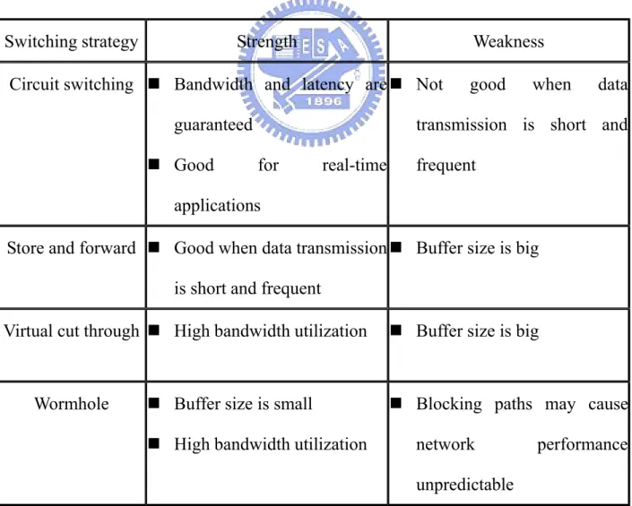
(15) The topology of the network is 2D mesh. The reasons why we choose it are three folds. First, as shown in [15], because of the simple connection and easy routing provided by adjacency, it is widely used in parallel computing platforms. Second, the interconnect length between nodes is uniform, which ensures the uniformity of the performance and overall scalability of the network. And last, it meets the inherent constraint of IC manufacturing technology. The way how data communication is carried out in the network is as follows: if a processor wants to pass information to any other processor, it sends information to the local switch. The switch then decides which adjacent switch is to receive the information. If the local processor of this switch is the destination, then the information is received by this processor; otherwise, the procedure just repeats until the information is sent to the destination.. 2.2 Switch Design. 2.2.1 Switching Strategies Before we get to know how our switch works, knowledge about common switching strategies is required. Common switching strategies can be classified into two categories: connection-oriented switching and connectionless switching [16]. For connection-oriented switching, also named circuit switching, a connection from the source to the destination is established before data transmission. Once the connection is established, the full bandwidth of the hardware path is available. Circuit switching is generally a good switching strategy if data transmission is long and infrequent. That is, when the time to establish the connection compared to the time to transmit data is 5.
(16) short, the strategy is advantageous. Since there is a dedicated connection of data transmission, the available bandwidth is known, meaning that the latency can be guaranteed—this is really good for real-time applications. But, when connection is reserved for the duration of one data transmission, other data transmission may not use resources occupied by the connection. This may degrade the overall network performance. Alternatively, for connectionless switching, data can be partitioned into packets. Each packet can be individually routed from the source to the destination without any connection reserved prior to data transmission. As a result, the bandwidth utilization is more efficient. Popular. packet. switching. strategies. include. store-and-forward,. virtual. cut-through and wormhole. For store-and-forward, a packet is completely buffered at each intermediate node before it can be forwarded to the next node. Compared to circuit switching, its performance is better when data transmission is short and frequent since it does not require the existence of dedicated connection. However, the switch implementation is expensive because the switch should have the capability to buffer a whole packet. Store-and-forward assumes that a whole packet must be available before it can be forwarded to the next node. This is not generally true, however, because the first few bytes of a packet may contain routing information. A switch can start forwarding information to the next node as soon as routing information of a packet is available. The switching technique which exploits this is referred to as virtual-cut-through. In the absence of blocking, the latency experienced by data transmission using this method is shorter, implying higher bandwidth utilization. On the other hand, if the header of a packet is blocked during data transmission, a packet can be completely buffered until it can be transferred. In this way, virtual-cut-through works just as 6.
(17) effectively as store-and-forward. Of course, the switch implementation is still expensive considering it has to buffer a whole packet. It’s difficult to construct a switch that is small, compact, fast, and capable of storing a whole packet. In wormhole switching, a packet is further decomposed into smaller units. In this way, a switch only has to be capable of storing a few units when data transmission is blocked. This suggests that the buffer requirement within a switch is substantially reduced over the requirements for virtual-cut-through. Hence, a switch can be much smaller and faster. However, when the head of a packet is blocked, the following parts of the packet cannot move on. This forms a blocking path and causes a pause in other data transmission in turn. Under this situation, latency of data transmission is unpredictable [17].. Switching strategy. Strength. Weakness. Circuit switching Bandwidth and latency are Not guaranteed Good. good. when. data. transmission is short and for. real-time. frequent. applications Store and forward Good when data transmission Buffer size is big is short and frequent Virtual cut through High bandwidth utilization. Wormhole. Buffer size is small High bandwidth utilization. Buffer size is big. Blocking paths may cause network unpredictable. Table 1 Comparison of different switching strategies. 7. performance.
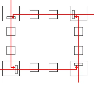
(18) Before we move on to next section, characteristics of all mentioned switching strategies are summarized in Table 1.. 2.2.2 Features of Our Switch Our switch has four important features. First, circuit switching is chosen because it does not require much memory. Usually, we don’t have too much memory on chip, for its size is large. Also, it supports real-time applications. This is not true for connectionless switching strategies. Then, we exploit the idea of virtual channel flow control [18]. If parts of data are buffered at the input or output of each physical channel, once a message occupies the buffer, no other messages can ever access that channel until it is released. Even worse, a situation named deadlock, a network state where no messages can advance because each message requires a physical channel occupied by other message, could happen. Figure 2 illustrates such a situation.. Figure 2 Deadlock. In fact, a physical channel can be divided into several unidirectional virtual 8.
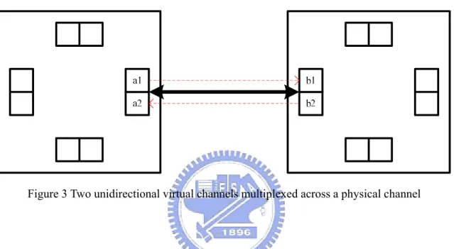
(19) channels, each realized as a pair of buffers multiplexed across a physical channel. For example, in Figure 3 buffer a1 and b1 form a unidirectional virtual channel flowing from a1 to b1; buffer b2 and a2 form another from b2 to a2. Assuming that these two virtual channels share the bandwidth of the physical channel equally, each virtual channel operates as if on a separate physical channel, only with half of the original bandwidth.. Figure 3 Two unidirectional virtual channels multiplexed across a physical channel. By dividing a physical channel into several virtual channels, messages can make progress rather than being blocked. For example, Figure 4 shows two messages crossing the physical channel between switch 1 and switch 2. Without virtual channels, one message may prevent the other from advancing, depending on which gets the privilege of the physical channel first. However, with virtual channels multiplexed across the physical channel, both messages continue to make progress at a rate which is half the achievable if there are no virtual channels. Since the time required for a message to wait until it is transferred is reduced, the average latency is decreased. As a result, the physical channel utilization rate is higher and the network throughput is increased. By continuing to add virtual channels, the overall message latency and network throughput can be improved further—at the cost of more buffer size and 9.
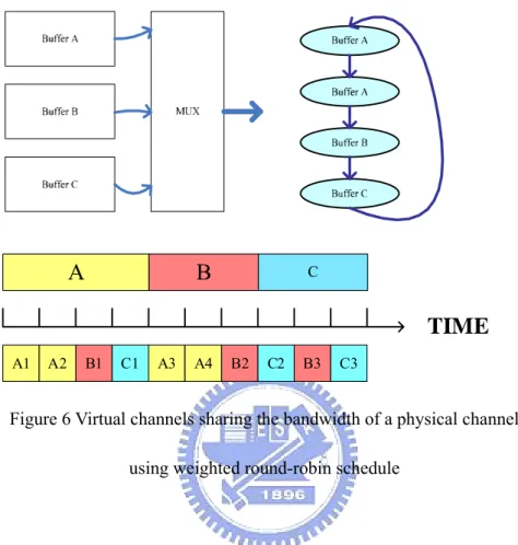
(20) complex multiplexer.. Figure 4 Messages make progress rather than being blocked. Third, although the bandwidth of a physical channel can be equally shared among all virtual channels, this is generally not a good idea. As shown in Figure 5, instead of sharing bandwidth equally, we use a round-robin schedule to grant rights to each virtual channel. Only when messages are to be transmitted over some virtual channels does our round-robin schedule give rights to them. Those virtual channels without data transmission cannot, and do not have to, access the physical channel.. Buffer A Buffer B Buffer C. A. B. C. TIME A1. B1. C1. A2. B2. C2. A3. B3. C3. A4. Figure 5 Virtual channels sharing the bandwidth of a physical channel using round-robin schedule 10.
(21) Moreover, if we find out there is heavy traffic over some virtual channels, we can grant privilege to them more frequently using weighted round-robin schedule shown in Figure 6. All we have to do is to configure our switch.. A. B. C. TIME A1. A2. B1. C1. A3. A4. B2. C2. B3. C3. Figure 6 Virtual channels sharing the bandwidth of a physical channel using weighted round-robin schedule. Last, for traditional networks, the number of nodes is not known and the behavior of communication is not predetermined. This is not true for on-chip networks, where the number of nodes and the behavior of communication can be known before run-time. Therefore, we can have dedicated connection paths established in advance by reserving the corresponding virtual channels for them. With proper configuration, our switching method acts just like circuit switching. Still, if demanded, we can allocate more bandwidth to some connection paths by using the weighted round-robin schedule mentioned above. This suggests that our switching technique can do the same thing as does circuit switching to support real-time applications. To summarize, features of our switch are listed below: 11.
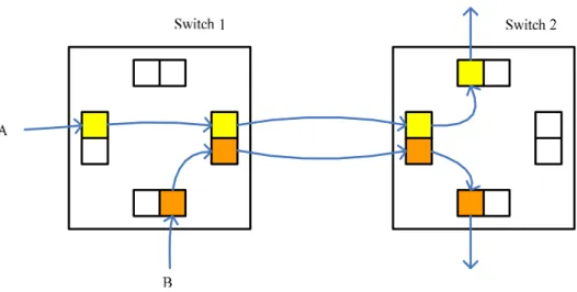
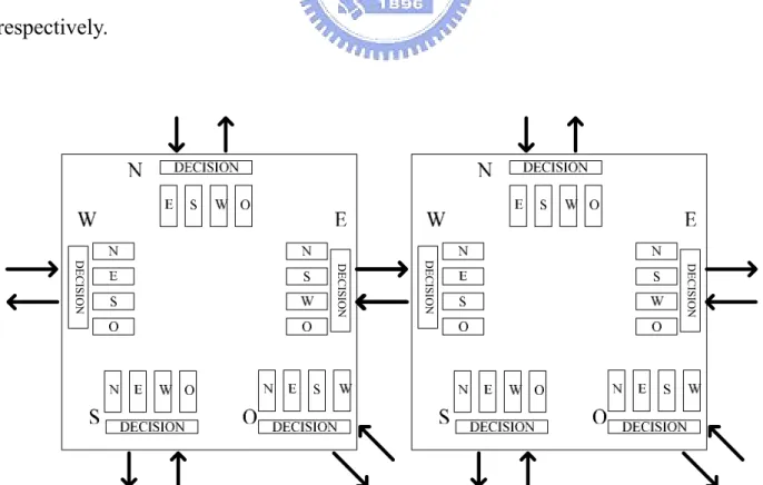
(22) . Small and fast. . Re-configurable. . Provides efficient bandwidth utilization. . Supports for real-time applications: dedicated connection paths can be reserved. . Bandwidth of each connection path can be configured. 2.2.3 Switch Model As shown in Figure 7, each switch has five pairs of input and output ports. Output ports at North (N), East (E), South (S), and West (W) connect to the corresponding input ports of the adjacent switches. The output port at E side of the left switch, for example, connects to the input port at W side of the right switch. The remaining output and input ports at O side connect to and from the local processor respectively.. 12. DECISION. DECISION. DECISION. DECISION. Figure 7 Inside the switch.
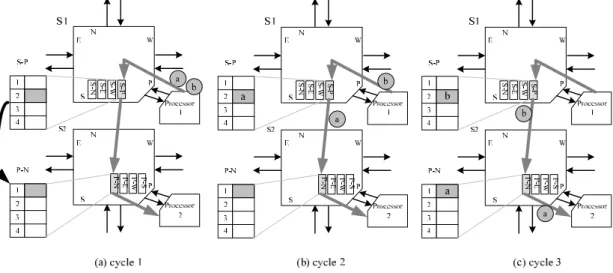
(23) There are four queues at each side. Each queue stores data ready to be transferred to and received from the adjacent switch. For the input part of a queue, the label on it indicates that the received data will be transferred later to that side of the switch. For instance, the input part of the queue labeled N at the E side of a switch stores data to the N side of the same switch. On the other hand, for the output part of a queue, the label on it indicates to which side the stored data is transferred in the adjacent switch. For example, the output part of the queue labeled S at the E side of a switch stores data that will later be transferred to the S side of the adjacent switch. As mentioned in 2.2.2, a physical channel can be divided into several virtual channels. Our switch supports four modes with channel width factors equal to 1, 2, 4, and 8 respectively. Here, the channel width factor indicates the maximum allowable number of virtual channels passing each input/output queue at each side of a switch. Since there are always four input and output queues at each side of a switch, the number of virtual channels connecting to the adjacent switch at each side are four times the channel width factor. Therefore, if the channel width factor is 2, there will be at most 8 virtual channels flowing out and 8 flowing in each side of a switch. Here, data is transmitted over pipeline buses. In Figure 8, a grey line indicates a transmission path from processor 1 to processor 2. Here, processor 1 is trying to send two packets ‘a’ and ‘b’ to processor 2. The transmission steps are as follows: first, in Figure 8(a), processor 1 sends ‘a’ to its local switch, S1; in the next cycle, ‘a’ is sent to S2 while ‘b’ is sent to S1 at the same time as shown in Figure 8(b); then in (c), ‘a’ arrives in its destination, processor 2, while ‘b’ is sent to S2; finally, ‘b’ also arrives at processor 2 at the fourth cycle, finishing the transmission.. 13.
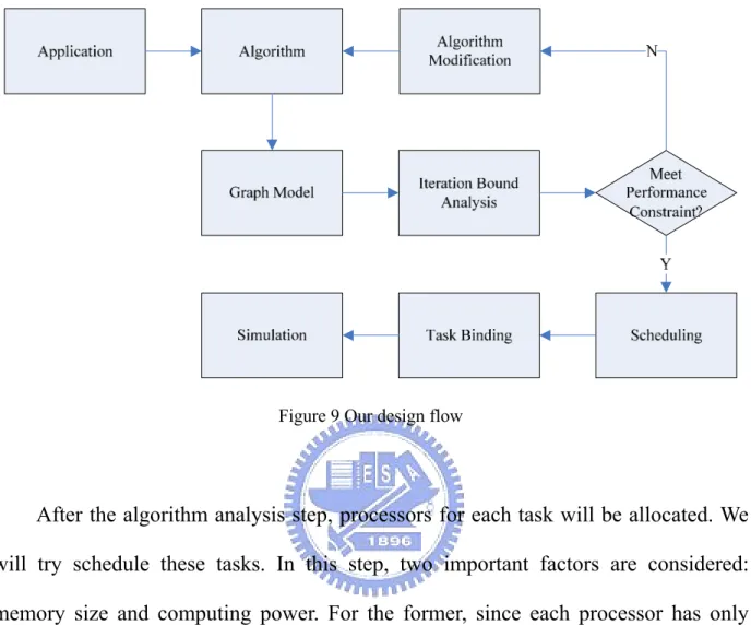
(24) Figure 8 Processor 1 sending two works to processor 2. Since details of a transaction are not our focus in the switch model, we only need to know that it takes three cycles for a packet to pass a virtual channel. Therefore, the latency experienced by each packet is three times the number of virtual channels it passes plus the time this packet waits when it is blocked. In worst case, the bandwidth available to this packet is the minimum one of all virtual channels it passes along the transmission path.. 2.3 Our Design Flow Figure 9 depicts our design flow that starts with an application. Initially, the algorithm for the application is chosen and partitioned into interacting tasks. Then, these tasks and their relationship will be modeled by a graph model. In this graph model, the computation and communication amount required for each individual task and paired tasks will be indicated. Since many algorithms contain feedback loops, an iteration bound, which is the lower bound on the achievable iteration period, will be imposed. It is not possible to achieve an iteration period less than the iteration bound, even when infinite resources are available. Here we will examine if our algorithm 14.
(25) meets the performance constraints. If not, we will modify and repartition the algorithm again, repeating the same procedure until those constraints are met.. Figure 9 Our design flow. After the algorithm analysis step, processors for each task will be allocated. We will try schedule these tasks. In this step, two important factors are considered: memory size and computing power. For the former, since each processor has only limited memory size, we must make sure that the required data for and the intermediate data generated by a task can be stored into a processor. For the latter, we wish to share task loads equally among the allocated processors so that no processor is idle while others are busy. By carefully handling these points, the system performance will be improved because each processor will be utilized to the maximum. The task binding process is performed next. In this step, we decide which task should be mapped onto which processors. The interacting tasks should be always mapped onto processors in the same region, reducing the time spent on their interaction. In our platform, dedicated connection paths reserved in advance are used when processors communicate. When assigning connection paths, we try best to find 15.
(26) the shortest path between each paired processors, while avoiding over usage of routing resources. Finally, all information generated will be collected and fed to our simulator. We can run some applications on our simulator to see if they work well on our platform.. 16.
(27) Chapter 3 Task Binding In this chapter, the task binding problem will be discussed. First, the problem formulation of task binding will be given in 3.1. Then our solution to the problem is presented in 3.2. Finally, details of the techniques we exploit to solve this problem will be shown in 3.3 and 3.4.. 3.1 Problem Formulation Task binding problem can be formulated as:. Given . Applications A1~Ak. . Corresponding task graph (directed-acyclic graph) Gi = G(V, E) for each application Ai. With . Each vertex vЄVi representing a task to run on one processor, and the amount of computation shown in the vertex. . Each edge eЄEi indicating data transmission along the arrow, and the amount of communication shown by the edge. . NVi representing total number of vertices in Gi, and NV representing the 17.
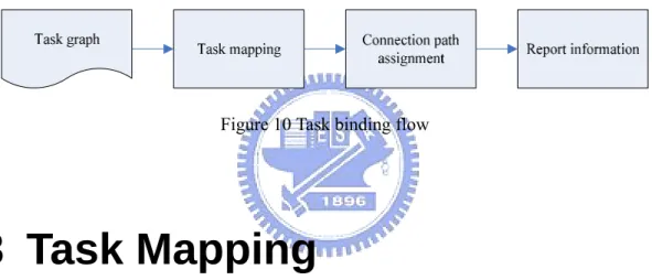
(28) summation of NVi; NV be less or equal to the number of processors available. We wish to . Map each vertex onto a processor. . Place connected tasks as close as possible to reduce interaction time. . Find a corresponding connection path for each edge. . Minimize the total routing resource requirement. 3.2 Task Binding Flow The process of task binding tries to find out a solution that every vertex in task graphs be mapped onto a processor, and for each pair of connected vertices, a connection path be reserved for communication. Here, because of the problem complexity, the process is divided into two parts. The former part of the process, task mapping, is analogous to placement problem in FPGA. But in our problem, instead of determining which logic block within an FPGA should implement each of the logic blocks required by the circuit, we decide which processor should execute which task. The latter part of the process, connection path assignment, does almost the same as does routing techniques in FPGA. In FPGA, there can be one source node and many sink nodes connecting to a signal wire. On the contrary, in our platform, only one source node and one sink node can be connected to the ends of a virtual channel. This is because it is data that we want to pass along a virtual channel, not voltages. In Figure 10, the flow of task binding is shown. First, a task graph containing the 18.
(29) computation/communication information for all tasks is given. Note that this task graph should be a directed-acyclic graph. After this, we exploit placement techniques used in FPGA to map tasks onto processors. If any two tasks communicate, processors in the same region will be allocated for these tasks. Then, we’ll reserve connection paths for these tasks. Therefore, when data transmission is to occur, pre-allocated and dedicated connection paths will be used. Finally, the position information of processor belonging to each task, the information of connection path for any two interconnected processors and the number of virtual channels needed across a physical channel will be reported.. Figure 10 Task binding flow. 3.3 Task Mapping The three major placers commonly in use today are min-cut, simulated annealing, and analytic based placers. Usually, the use of analytic based placers is often followed by iterative improvement [19]. Since design of architecture of on-chip-networks is an important issue, we wish to explore much different architecture. Thus, the optimization goals of our placer may change from architecture to architecture. Among the three types of commonly used placers, the simulated annealing based placer can be more easily adapted to new optimization goals than min-cut and analytic based placers [20]. Therefore, we use simulated-annealing technique to map tasks onto processors.. 19.
(30) 3.3.1 Simulated Annealing Simulated annealing proposed in [21] is a widely used heuristic to solve several combinatorial optimization problems including many well known CAD ones. It belongs to the class of non-deterministic algorithms. As its name suggests, simulated annealing mimics the annealing process used to gradually cool molten metal to produce high-quality metal objects. During the process, a metal is heated to a very high temperature and then slowly cooled down. At some proper cooling rate, the process has a very good chance of producing high-quality metal objects. If we compare optimization to the annealing process, the attainment of a good solution is analogous to that of refined metal objects. For a combinatorial optimization problem, we wish to find out solutions with low costs in the solution space, which is a set containing all possible solutions. Some of these solutions correspond to local optima, while others may be global optima. In Figure 11, the solutions are shown along the x-axis. It is assumed that two consecutive solutions are local neighbors, which are solutions that can be reached from the original one with only a slight change. The cost of solution grows in the positive direction along the y-axis. Here, S1, S2, and L are local optima since all the local neighbors have higher and thus inferior costs. Among these three solutions, L, also called global optimum,. has the minimum cost.. The process of an iterative improvement scheme starts with an initial solution. Then the solution is refined again and again. Finally the procedure stops if it finds an optimum solution. For a greedy algorithm, if we start with an initial solution, say I in Figure 11, we gradually slide down the “hill” because the costs there are lower and stop once we reach S1. Although S1 is the best solution we can ever find, it is still a local optimum solution. The initial solution given prevents us from the global 20.
(31) optimum solution. There is no way for a greedy algorithm to find the global minimum solution under this situation, unless it “climbs the hill”.. Cost. I. S1 S2 L. Solution Space. Figure 11 Local versus global optima. Simulated annealing is such a hill-climbing algorithm. This time the algorithm starts again with the initial solution I and examines its neighborhood. If a neighboring solution has a lower cost, it is always accepted. On the contrary, if a neighboring solution is worse, the algorithm occasionally accepts this inferior solution, since there may be times that the algorithm finds a better solution once it goes beyond the hill. By doing so, the algorithm escapes from getting stuck at a local optimum solution S1. Pseudo-code for a generic simulated annealing based placer is shown in Figure 12. Here, a cost function is defined to assess the quality of the solution. We start with an initial solution by mapping tasks randomly onto processors. Then, a large number of swaps are made within a region, specified by the range limiter R, to gradually improve the solution and the change in cost is calculated. The swap is always accepted should the cost decrease. Otherwise, it still has a chance to be accepted. The probability of acceptance is given by e − Diff / T , where Diff is the change in cost a change makes, and T is a parameter called temperature that controls the likelihood of 21.
(32) accepting moves. Initially, T is very high, which suggests that any move will be easily accepted. Then, it is gradually decreased as the solution is refined. Eventually, the probability of accepting a move that makes the solution worse will be very low.. Figure 12 Pseudo-code for generic simulated annealing placer. 3.3.2 Cost Function In FPGA placement, a placer usually tries to minimize the total wiring (wire-length driven), places blocks so as to balance the wiring density (routability-driven), or to maximize system performance (timing-driven). For a wire-length driven placer, estimation of wire length can be done by using the semi-perimeter method [19]. The method tries to find the smallest bounding box that encloses all the pins to be connected. The estimated wire length is half the perimeter of this rectangle. For example, in Figure 13, the estimated wire length is 9.. 22.
(33) Figure 13 A bounding box. Since in our problem a connection path always connects to only two processors, the semi-perimeter method accurately calculates the distance that the transmitted data would travel. Therefore, if we let the cost of a solution be the summation of all distances between each paired processors, and try to minimize the cost, any pair of connecting processors will be placed as close as possible.. 3.3.3 Annealing Schedule The rate at which the temperature is decreased, the exit criterion to terminate the process, the number of moves attempted at each temperature, and the method by which potential swaps are made are defined by the annealing schedule. A good annealing schedule is essential to make sure high quality solution obtained in a reasonable time. Because we still wish to explore much different architecture, the optimization goals of our placer may change from architecture to architecture. Therefore, a good fixed annealing schedule is still not enough. We need a schedule that automatically adapts to new architecture, no matter what our cost function is. Here we incorporate some best features from [20], [22], [23], and [24]. First, an initial solution is generated and some swaps are made. The initial 23.
(34) temperature is set to twenty times the standard deviation of the costs of these swaps [22]. The temperature is gradually adjusted to stay around a productive temperature where a significant fraction of swaps that makes improvement over the original solution are accepted [20]. Second, the number of moves attempted at each temperature is determined by a function of the number of processors, since the number of processors differs from case to case [24]. Then, the region within swaps are made is adjusted to keep the fraction of swaps accepted around 0.44 for as long as possible [23]. Finally, the procedure terminates when the temperature is less than some small fraction of the average cost of the solutions the algorithm examined [20]. Since detail of the annealing schedule is not our focus, we omit them from this thesis.. 3.4 Connection Path Assignment. 3.4.1 Pathfinder Algorithm Once processors for all the tasks have been chosen, a router tries to assign connection paths between any pair of interconnected processors. Here, we use the router algorithm like the one proposed in [25] to solve this problem. This router is essentially a variant of maze router [26]. It runs Dijkstra’s algorithm [27] to find the shortest, the lowest cost, path between a sender and a receiver processor. The Pathfinder algorithm [25] then performs a multiple of routing iterations to rip up some or all nets and reroute them by different paths, in case there is a competition for routing resources that makes the routing illegal. However, note that ripping up and rerouting these nets only affect the net ordering. These nets are all routed by the same maze routing algorithm. 24.
(35) The cost of using a routing resource n is defined in [25] as: Cost (n) = [b(n) + h(n)] × p(n) , and pseudo-code for the Pathfinder algorithm is shown in Figure 14. The Pathfinder algorithm exploits the idea from Nair [28] to repeatedly rip up and reroute every path until all congestion is resolved. Ripping-up and rerouting every net once is called a routing iteration. During the first iteration, every path is routed for minimum cost, even if this leads to overuse of some routing resources. However, a routing in which some resources are overused is not a legal solution. As a consequence, when overuse exists at the end of a routing iteration, more iteration must be performed to resolve this situation. During each iteration, the present congestion cost, p(n), will be updated every time a path is ripped-up and rerouted. At the end of each iteration, the historical congestion cost, h(n), of overusing a routing resource is updated to record the severity of historical congestion over this routing resource. Therefore, it is less probable for the router algorithm to find a path passing this resource in the next iteration. As a result, all congestion will be gradually resolved.. Figure 14 Pseudo-code for Pathfinder algorithm. 25.
(36) 3.4.2 Routing Resource Graph The internal representation we incorporated here should be as architecture independent as possible, so we can easily describe different architecture without making any change to the algorithm. Here we use routing resource graph representation [25] to describe architecture internally. In routing resource graph representation, processors and buffers over virtual channels become nodes. Virtual channels become directed edges, indicating that data over them flows unidirectionally. For each node, a capacity is assigned to specify the maximum number of different paths that can use this node in a legal routing. And the number of different paths currently using each node is indicated in the occupancy field. Since potential connections all become edges in a routing resource graph, routing a connection corresponds to finding a path in the graph, starting from a SOURCE node to a SINK node. Figure 15 illustrates how the part of the routing resource graph between a processor and its local switch is constructed. For data flowing out the processor, it starts at a SOURCE node and flows to the OUT node. After it arrives at the OUT node, it chooses to which one of the four SW_IN nodes it will go. Here, the label indicated in each SW_IN node suggests that this node will later connect to the SW_OUT node at that side of the switch.. 26.
(37) DECISION. DECISION. Figure 15 Routing resource graph for a processor and its local switch. Since data flowing into the processor may come from any of the four sides of the local switch, there are four corresponding SW_OUT nodes, each connecting to the IN node. The IN node then connects to the SINK node. Once data arrives the SINK node, its journey stops. Here, the capacity of each SW_IN or SW_OUT type node is set equal to the channel width factor. The channel width factor is the maximum allowable number of paths passing these two type nodes. If the channel width factor is four, at most four connection paths may pass any of these nodes. Because data on these nodes may flow into or out SOURCE, OUT, IN, SINK type nodes, the capacity of each these nodes is four times the channel width factor. Figure 16 shows how the part of the routing resource graph inside a switch is constructed. For reason of clarity, we only show edges to and from the local processor. After data flows out from the local processor, it can choose to go to the adjacent switch at any side. This is modeled by four pairs of SW_IN and SW_OUT nodes. On 27.
(38) the contrary, the situation that data can flow from the adjacent switch at each side is modeled by another four pairs of SW_IN and SW_OUT nodes.. DECISION. DECISION. Figure 16 Routing resource graph for a switch. Finally, Figure 17 shows the part of the routing resource graph that will be used when data flows to and from the adjacent switches. In this figure, the data transmitted to the left switch is from any of the four SW_OUT nodes labeled W at the W side of the right switch. A CHANX type node whose capacity is four times the channel width factor is then passed. And, data goes to any of the four SW_IN nodes at the E side of the left switch. If the one labeled N is chosen, for example, data will go to the corresponding SW_OUT node at the N side of the left switch.. 28.
(39) N. W. S. W. CHAN X. O. W. W. W. I N. O U T. O U T. I N. E E E. N CHAN X. E. E O S. Figure 17 Routing resource graph across a physical channel. 3.4.3 Cost Function Here we define the cost of a routing resource somewhat differently than [25]. The cost of using routing resource, n, is defined as:. Cost (n) = b(n) × h(n) × p (n) , where b(n), h(n), and p(n) are the base cost, historical congestion, and present congestion terms mentioned in 3.4.1. Instead of adding b(n) and h(n) together, we multiply them. When adding terms together in cost function, it is very important to make sure that they are properly normalized to the same range of magnitude so that both terms work effectively. We avoid this by multiplying them together. The base cost of a node, b(n), is set to reflect the latency that data transmission will experience when passing this node. A router is encouraged to use as few nodes as possible to route each connection path. Table 2 shows the base cost for each type of routing resource. Note that no matter what exact cost is chosen for each type of 29.
(40) routing resource, the router always makes sure that no routing resource is overused. This is guaranteed by the congestion avoidance factors, h(n) and p(n), in the cost function.. Resource Type. Base Cost. SOURCE, OUT. 0. SW_IN, SW_OUT. 1. CHANX, CHANY. 2. IN, SINK. 0. Table 2 Base cost for each type of routing resource. In fact, SW_IN is a node that does not really exists in our switch. However, since there is only one possible connection from a routing resource of type SW_IN to its corresponding SW_OUT type resource, we can set both their costs to 1, which is half the value of cost for CHANX or CHANY type resource. Somehow, if we set costs of SW_IN and SW_OUT type node to 0 and 2, the router performance will degrade, since the cost of SW_IN will always be 0 no matter what value h(n) and p(n) are. This suggests that our router may not be aware of congestion problem on SW_IN type node and may spend more time to resolve resource congestion problem. On the other hand, since the maze expansion used to route a connection path always begins with a pair of SOURCE and OUT type nodes, the exact costs set for them do not matter. We set them to zero to save some computation. Also, the expansion terminates when it reaches a pair of IN and SINK type node. By setting their costs to zero, some CPU savings can be obtained because the maze expansion tends to stop earlier before it expands further.. 30.
(41) The present congestion penalty is updated whenever any net is ripped-up and re-routed according to. p(n) = 1 + max(0, [occupancy(n) + 1 − capacity(n)]) × p fac ) , where occupancy(n) is the number of connection paths currently using routing resource n and capacity(n) is the maximum allowable number of paths that can legally use node n. The historical congestion factor is updated only after an entire routing iteration. Its value during routing iteration i is: h( n ) i =. 1 h(n) i −1 + max(0, [occupancy(n) − capacity(n)] × h fac ). i =1 i >1. The value of hfac can be kept constant for all routing iterations. The fact that h(n) increments after each iteration already provides sufficient increase in the historical congestion factor. As for pfac, the higher the value, the faster the speed that can be reached when resource congestion problem happens in a routing iteration. However, if it is assigned a small value initially and gradually incremented from iteration to iteration, a better routing quality is obtained. The router under this condition will try to solve congestion problem while maintaining all connection paths short.. 31.
(42) Chapter 4 Experimental Results. 4.1 Experiment Flow Figure 18 shows our experiment flow. First, we exploit Task Graph For Free (TGFF) [29], a user-controllable, general-purpose, pseudorandom task graph generator, to generate many random cases. Then, we extract some information from the generated cases and pass them to our task binding tool. After each task is mapped onto a processor and each connection path is assigned, we incorporate the routing information with our platform simulator and run simulation. Finally, we use some scripts to extract important parameters from the log file and analyze these data.. Figure 18 Our experiment flow 32.
(43) For each case we generated, there will be 1 to 5 independent task graphs, each containing at least 4 to 20 tasks. The maximum number of inputs/outputs of each task is from 2 to 10. Each case is composed of many nodes and arcs. A node represents a task to be run on one processor. An arc drawn from one node to another node indicates that communication exists between these two nodes, flowing from the former to the latter. The amount of computation of a node and the amount of communication of an arc will also be indexed by the numbers shown by the corresponding entries. The mapping between TGFF output file and its corresponding task graph is shown in Figure 19.. TASK t0_0 TASK t0_1 TASK t0_2 TASK t0_3 TASK t0_4 TASK t0_5 TASK t0_6 TASK t0_7 ARC a0_0 ARC a0_1 ARC a0_2 ARC a0_3 ARC a0_4 ARC a0_5 ARC a0_6. TYPE 0 TYPE 1 TYPE 2 TYPE 3 TYPE 4 TYPE 5 TYPE 6 TYPE 7. Computation Amount. FROM t0_0 TO t0_1 TYPE 36 FROM t0_1 TO t0_2 TYPE 24 FROM t0_1 TO t0_3 TYPE 10 FROM t0_0 TO t0_4 TYPE 2 FROM t0_4 TO t0_5 TYPE 47 FROM t0_4 TO t0_6 TYPE 18 FROM t0_4 TO t0_7 TYPE 12. Communication Amount. Figure 19 Mapping between output of each case and its corresponding task graph. Our simulator uses two component models: the processor model and the switch model described in 2.2.3. In our processor model, we assume that a processor begins to operate only when all input data is available and the output buffer size is enough for data that will be later generated. For example, the processor allocated for the task shown in Figure 20 requires two input I0 and I1 from the preceding processors. Once 33.
(44) it gets all the data, the processor checks to see if the buffer size is enough for output data that will be later generated. If so, it begins to operate and puts all output data into the buffer. The corresponding switches then start to send these data to the subsequent processors.. Figure 20 A task with two inputs and three outputs. 4.2 Experimental Results. 4.2.1 Routability Analysis In our platform the minimum channel width factor required is determined by the maximum number of inputs or outputs of all tasks. (The channel width factor indicates the maximum allowable number of virtual channels passing each input/output queue at each side of a switch.) If a task requires five inputs, there is no way for a switch with a channel width factor one to support them because only four connection paths flowing into the corresponding processor could be established. As shown in Figure 21, among the generated 765 cases, only 7 cases require a 34.
(45) channel width factor of 4; and 4 cases, a factor of 6. A platform with a channel width factor of 3 will be able to support all other cases. This suggests that the switch cost can be very small, if the requirement for applications fall into the range of the. Number of Occurence. generated cases.. 400 350 300 250 200 150 100 50 0. 355 241 157. 1. 2. 3. 7. 4. 4. 6. Channel Width Factor. Figure 21 Requirement of channel width factor over 765 cases. 4.2.2 Performance Analysis In our experiment, we assume that the computation amount for a task is the number of cycles the allocated processor takes when it runs this task. Also, if the bandwidth of each physical channel is one unit, we assume that a data transmission runs a minimum of N cycles (under ideal condition), N equaling to the communication amount indicated in the task graph. After simulation, we collect information from the output file, calculate the performance gain of the system and count the utilization rate of each processor. The equations for system performance gain and processor utilization rate are listed in the 35.
(46) shaded box in Figure 22. If an application composed of many tasks runs on only one processor, the total time E required to run this application once will be the summation of the computation time of all tasks. Suppose that the computation load is distributed on N processors. The performance gain will be the system throughput T times E, divided by the number of simulation cycles S. And the utilization rate for each processor will be the performance gain divided by N. Note that in Figure 22 the number of times a task has been executed in S cycles is indicated in the circle. For this case, the system throughput equals to 7.. 10. 9. S = Simulation Cycle E = Execution Time on One Processor T = System Throughput N = Number of Processors. 8. Performance Gain = T*E/S Processor Utilization Rate = T*E/S/N. 7. Figure 22 Performance measurement. We experiment on 765 different cases with different communication loads. The computation amount is set to an average of 200, with minimum and maximum value equal to 100 and 300. The communication amount is set the same way when the ratio of computation to communication equals to 1. Note here that the ratio is defined to be the average computation amount divided by the average communication amount. The relationship between communication load and average processor utilization 36.
(47) rate is shown in Figure 23. Note that if we set the ratio to a value greater than 4, the average processor utilization rate will be higher than 0.6. However, if the communication load is heavier, say with a ratio below 3, the average processor utilization rate falls quickly. This is not a favorable situation. To overcome this problem, a designer may choose a system with greater physical channel bandwidth. For example, if a system with a ratio equal to 2 is run on a platform with the original physical channel bandwidth doubled, the average processor utilization rate will be improved from an average value below 0.5 to an average value higher than 0.6.. Average Processor Utilization Rate. 0.8 0.7 0.6 0.5 0.4 0.3 0.2 0.1 0 0. 2. 4. 6. 8. 10. 12. Ratio of Computation to Communication Figure 23 Relationship between communication load and processor utilization rate. 4.2.3 Scalability Analysis If an application has a maximum number of inputs or outputs greater than 4, there must be some physical channels shared by at least two virtual channels. Therefore, some input/output data is not transmitted at full speed to the subsequent 37.
(48) tasks. Having to wait longer, these tasks lower the system performance. Here we experiment on 765 tasks with a computation to communication ratio of 3. The reason why 3 is chosen is because the impact of maximum degree of inputs or outputs is apparent when communication load is heavy. Otherwise it is not that clear, since there is little traffic on the platform if the communication load is low. In Figure 24, the straight line drawn from the left to the right predicts the processor utilization rate, as a function of the number of processors on the platform. With nearly 70 tasks distributed on our platform under such a heavy communication load, the processor utilization rate still maintains above 0.5. This is because only few physical channels are shared with the maximum number of inputs or outputs equal to 4.. 0.9. Average Processor Utilization Rate. 0.8 0.7 0.6 0.5 0.4 0.3 0.2 0.1 0 0. 10. 20. 30. 40. 50. 60. 70. 80. Number of Processors. Figure 24 Experiment with the maximum number of inputs or outputs equal to 4. On the other hand, the scalability of our platform is not good with maximum number of inputs or outputs equal to 7. In Figure 25, the straight line predicts the processor utilization rate when the number of processors grows. With about 70 tasks distributed on our platform, only processor utilization rate below 0.4 is achievable; 38.
(49) should more tasks be mapped onto the platform, the processor utilization rate may be worse.. 0.9 Average Processor Utilization Rate. 0.8 0.7 0.6 0.5 0.4 0.3 0.2 0.1 0 0. 10. 20. 30. 40. 50. 60. 70. Number of Processors. Figure 25 Experiment with the maximum number of inputs or outputs equal to 7. 39. 80.
(50) Chapter 5 Conclusion and Future Work In this work, the task binding problem is formulated and solved by techniques similar to those of placement and routing in FPGA. By incorporating the processor model, the switch model and the connection path information generated by our task binding tool, systems with different configurations can be simulated in a short time. Some important parameters are then extracted from the simulation output file and the performance of the system can be assessed before the system is implemented. In Chapter 4, performances of systems with different configurations are examined. The results show that the scheduling process discussed in 2.3 must not only take computing power and memory size of each processor into consideration, but they also have to pay close attention to the maximum number of inputs/outputs and the communication load of the system. With our simulation environment feeding back important factors, we wish to find an algorithm to solve the scheduling problem `systematically and efficiently. Also, the buffer size at the input/output of a processor has impact on the system performance. If the buffer size is unlimited, data transmission always finishes as soon as possible since there is always space for data inside a processor. However, since on-chip memory is very expensive, this can never be fulfilled. We wish to solve the problem so that the total buffer size is minimized while the system performance is maintained. Last, since virtual channels may work at full bandwidth of the physical channel if 40.
(51) no other data is transmitted along these virtual channels at the same time. We wish to elaborate an accurate model of traffic contention and improve our task binding algorithm further so that each processor can be utilized to the ultimate. In this way, higher system performance can then be achieved without having to add any resource.. 41.
(52) Reference [1] Axel Jantsch, and Hannu Tenhunen, Networks on Chip, Kluwer Academic Publishers, 2003 [2] Adrijean Adriahantenaina, Hervé Charlery, Alain Greiner, Laurent Mortiez and Cesar Albenes Zeferin, “SPIN: a scalable, packet switched, on-chip micro-network,” in Proceedings of the Design, Automation and Test in Europe Conference and Exhibition, 2003, supplements 70 – 73 [3] Cesar Albenes Zeferino and Altamiro Amadeu Susin, “SoCIN: a parametric and scalable network-on-chip,” in Proceedings of the 16th Symposium on Integrated Circuits and Systems Design, 2003, pages 169 – 174 [4] Partha Pratim Pande, Cristian Grecu, Andre Ivanov and Res Saleh, “Design of a switch for network on chip applications,“ in Proceedings of the 2003 International Symposium on Circuits and Systems, 2003, volume 5, pages 217 – 220 [5] Luca Benini and Giovanni De Micheli, “Networks on chips: a new SoC paradigm,” in Computer , 2003, volume 35, issue 1, pages 70 -78 [6] Shashi Kumar, Axel Jantsch, Juha-Pekka Soininen, Martti Forsell, Mikael Millberg, Johny Öberg, Kari Tiensyrjä and Ahmed Hemani, “A network on chip architecture and design methodology,“ in Proceedings of the IEEE Computer Society Annual Symposium on VLSI, 2002, pages 105 – 112 [7] Daniel Wiklund and Dake Liu, “SoCBUS: switched network on chip for hard real time embedded systems,” in Proceedings of the International Parallel and Distributed Processing Symposium, 2003, pages 78 – 85 [8] Doris Ching, Patrick Schaumont and Ingrid Verbauwhede, “Integrated modeling 42.
(53) and generation of a reconfigurable network-on-chip,” in Proceedings of the 18th International Parallel and Distributed Processing Symposium, 2004, pages 139 – 145 [9] Marcello Coppola, Stephane Curaba, Miltos D. Grammatikakis, Giuseppe Maruccia and Francesco Papariello, “OCCN: a network-on-chip modeling and simulation framework,” in Proceedings of the Design, Automation and Test in Europe Conference and Exhibition Designers’ Forum, 2004, volume 3, pages 174 – 179 [10] Robert Siegmund and Dietmar Muller, “Efficient modeling and synthesis of on-chip communication protocols for network-on-chip design,” in Proceedings of the 2003 International Symposium on Circuits and Systems, 2003, volume 5, pages 81 – 84 [11] Jan Madsen, Shankar Mahadevan, Kashif Virk and Mercury Gonzalez, “Network-on-chip modeling for system-level multiprocessor simulation,” in Proceedings of the 24th IEEE International Real-Time Systems Symposium, pages 265 – 274 [12] Kenichiro Anjo, Yutaka Yamada, Michihiro Koibuchi, Akiya Jouraku and Hideharu Amano, "BLACK-BUS: a new data-transfer technique using local address on networks-on-chips," in Proceedings of the 18th International Parallel and Distributed Processing Symposium, 2004, pages 10 – 17 [13] Mikael Millberg, Erland Nilsson, Rikard Thid, Shashi Kumar and Axel Jantsch, "The Nostrum backbone - a communication protocol stack for networks on chip," in Proceedings of the 17th International Conference on VLSI Design, 2004, pages 693 – 696 [14] Tang Lei and Shashi Kumar, “A two-step genetic algorithm for mapping task graphs to a network on chip architecture,” in Proceedings of the Euromicro 43.
(54) Symposium on Digital System Design, 2003, pages 180 – 187 [15] William J. Dally, “Performance analysis of a k-ary n-cube interconnect networks,” in IEEE Transactions on Computers, 1990, pages 775 – 785 [16] Jose Duato, Sudhakar Yalamanchili, Lionel Ni and Lionel M. Ni, Interconnection Networks: An Engineering Approach, Institute of Electrical & Electronics Enginee, 1997 [17] Li-Shiuan Peh and William J. Dally, “A delay model and speculative architecture for pipelined routers,” in The 7th International Symposium on High-Performance Computer Architecture, 2001, pages 255 – 266 [18] William J. Dally, “Virtual-channel flow control,” in Proceedings of the 17th Annual International Symposium on Computer Architecture, 1990, pages 60 – 68 [19] Sadiq M. Sait and Habib Youssef, VLSI Physical Design Automation: Theory and Practice, World Scientific Publishing Company, 1999 [20] Vaughn Betz, Jonathan Rose, Alexander Marquardt, Architecture and CAD for deep-submicron FPGAs, Kluwer Academic Publishers, 1999 [21] S. Kirkpatrick, C. D. Gelatt Jr. and M. P. Vecchi, “Optimization by simulated annealing,” in Science, 1983, volume 220, pages 498 – 516 [22] MD Huang, Fabio Romeo and Alberto Sangiovanni-Vincentelli, “An efficient general cooling schedule for simulated annealing,” in International Conference on Computer-Aided Design, 1986, pages 381 – 384 [23] Jimmy Lam and Jean-Marc Delosme, “Performance of a new annealing schedule,” in Proceedings of the 25th ACM/IEEE Design Automation Conference, 1988, pages 306 – 311 [24] William Swartz and Carl Sechen, “New algorithms for the placement and routing of macro cells,” in International Conference on Computer-Aided Design, 1990, pages 336 – 339 44.
(55) [25] Carl Ebeling, Lary McMurchie, Scott A. Hauck and Steven Burns, “Placement and routing tools for the Triptych FPGA,” in IEEE Transactions on Very Large Scale Integration Systems, 1995, pages 473 – 482 [26] C. Y. Lee, “An algorithm for path connections and its applications,” in IRE Transactions Electron Computing, 1961, volume EC 10, pages 346 – 365 [27] E. Dijkstra, “A note on two problems in connexion with graphs,” in Numerical Math, 1959, volume 1, pages 269 – 271 [28] Ravi Nair, “A simple yet effective technique for global wiring,” in IEEE Transactions on Computer-Aided Design of Integrated Circuits and Systems, 1987, pages 165 – 172 [29] Robert P. Dick, David L. Rhodes and Wayne Wolf , “TGFF: task graphs for free,” in Proceedings of the 6th International Workshop on Hardware/Software Codesign, 1998, pages 97 – 101. 45.
(56) VITA Chih-Chieh Chou was born in Taipei, Taiwan on November 28, 1979. He received the B.S. degree in Electronics Engineering from National Chiao Tung University in June 2002 and entered the Institute of Electronics, National Chiao Tung University in September 2002. His research interests include electronic design automation (EDA) and VLSI design. He received the M.S. degree from National Chiao Tung University in July 2004.. 46.
(57)
數據
+7
相關文件
– The The readLine readLine method is the same method used to read method is the same method used to read from the keyboard, but in this case it would read from a
• Suppose the input graph contains at least one tour of the cities with a total distance at most B. – Then there is a computation path for
FPPA 是 Filed Programmable Processor Array 的縮寫,簡 單的說:它就是一個可以平行處理的多核心單晶片微控器。與一般 微控器如 8051、pic,…
Only the fractional exponent of a positive definite operator can be defined, so we need to take a minus sign in front of the ordinary Laplacian ∆.. One way to define (− ∆ ) − α 2
The natural structure for two vari- ables is often a rectangular array with columns corresponding to the categories of one vari- able and rows to categories of the second
• A knock-in option comes into existence if a certain barrier is reached.. • A down-and-in option is a call knock-in option that comes into existence only when the barrier is
• A knock-in option comes into existence if a certain barrier is reached?. • A down-and-in option is a call knock-in option that comes into existence only when the barrier is
• A knock-in option comes into existence if a certain barrier is reached.. • A down-and-in option is a call knock-in option that comes into existence only when the barrier is
