行政院國家科學委員會專題研究計畫 期中進度報告
次 32 奈米 CMOS 元件可靠性分析,量子結構效應,與蒙地
卡羅電荷傳輸模擬(第 1 年)
期中進度報告(精簡版)
計 畫 類 別 : 個別型 計 畫 編 號 : NSC 96-2628-E-009-165-MY3 執 行 期 間 : 96 年 08 月 01 日至 97 年 07 月 31 日 執 行 單 位 : 國立交通大學電子工程學系及電子研究所 計 畫 主 持 人 : 汪大暉 計畫參與人員: 博士-兼任助理人員:唐俊榮 博士-兼任助理人員:邱榮標 博士-兼任助理人員:馬煥淇 碩士-兼任助理人員:邱子華 碩士-兼任助理人員:林彥君 碩士-兼任助理人員:趙元鵬 碩士-兼任助理人員:熊勖廷 處 理 方 式 : 期中報告不提供公開查詢中 華 民 國 97 年 05 月 26 日
次 32 奈米 CMOS 元件可靠性分析,量子結構效應,
與蒙地卡羅電荷傳輸模擬(1/3)
Sub-32nm CMOS Device Reliability, Quantum Structure Effects and
Carrier Transport Simulation by Using a Monte Carlo Method (1/3)
計畫編號:96-2628-E-009-165-MY3 執行期間:96 年 08 月 01 日 至 97 年 07 月 31 日 主持人:汪大暉 交通大學電子工程系教授 中文摘要 利用自行組裝之量測電路於高介電常數閘極 介電層之研究,吾人發現有不規則之負偏壓溫 度不穩定性。在某種加壓加溫之條件下,觀察 到汲極電流增加之行為。且隨著時間和電壓變 化時,汲極電流產生反轉之現象。吾人也發現 在 p 型電晶體中加壓後之電流衰減以及 n 型電 晶體中加壓後之電流回復之現象。吾人提出一 物理模型—雙極性電荷捕捉,來解釋實驗現 象;最後,由於雙極性電荷捕捉,吾人發現在 加壓之後單一電子和電洞自高介電常數閘極 介電層的缺陷中散逸之行為。同時藉由電荷幫 浦實驗及載子分離等實驗來驗證物理模型之 正確性。最後,評估負偏壓溫度不穩定性之電 壓、溫度、及時間因素對汲極電流之影響。 Abstract
Negative bias-temperature (NBT) stress induced drain current instability in a pMOSFET with a HfSiON-SiO2 gate stack is investigated by using a fast transient measurement technique. We find that in certain stress conditions the NBT induced current instability evolves from enhancement mode to degradation mode, giving rise to an anomalous turn-around characteristic with stress time and stress gate voltage. Persistent
post-stress drain current degradation is found in a pMOSFET, as opposed to drain current recovery in its n-type MOSFET counterpart. A bipolar charge trapping model along with trap generation in a HfSiON gate dielectric is proposed to account for the observed phenomena. Post-stress single charge emissions from trap states in HfSiON are characterized. Charge pumping and carrier separation measurements are performed to support our model. The impact of NBT stress voltage, temperature and time on drain current instability mode is evaluated.
Index Terms: HfSiON, negative bias temperature instability, bipolar charge trapping, single charge emission
I. Introduction
NBT instability has been recognized as a major reliability concern in ultra-thin gate dielectric MOSFETs. It occurs in p-type devices and manifests itself as negative shifts of threshold voltage due to positive oxide charge trapping under negative gate voltage stressing. As compared to a SiO2 gate dielectric, the NBTI in high permittivity (high-k) gate dielectric MOSFETs has been less explored. In previous
NBTI studies [1-3], a conventional “stress-and-sense” method was used, which introduces a switching delay between stress and sense up to a few seconds. For high-k gate dielectrics such as HfSiON, a significant post-stress transient effect was reported due to high-k dielectric charge trapping/detrapping. The ignorance of high-k charge trapping/detrapping in a switching delay may lead to an erroneous interpretation of measurement data and underlying physical mechanisms. Thus, to retrieve the important information between stress and sensing, a fast transient measurement technique [4,5] with a resolution of microseconds is employed in this work. By using this technique, the mode of the NBT induced drain current instability is characterized. Both current enhancement and degradation modes are observed in a HfSiON pMOSFET. A physical model based on bipolar charge trapping and trap generation in a high-k gate dielectric is proposed to explain the instability modes.
The devices used here are p-type MOSFETs with a polysilicon electrode and a HfSiON-SiO2 gate stack. The gate length ranges from 0.08 m to 1.2 m, and the gate width ranges from 0.16 m to 10 m. The physical thickness of the high-k layer and the interfacial SiO2 layer (IL) is 2.5nm and 1.4nm, respectively. The equivalent oxide thickness is 1.8nm. Detailed fabrication process and device characteristics were reported in [6,7]. To reduce the switching delay in characterization, our measurement system is computer-automated, including high-speed switches, an operational amplifier, and a digital oscilloscope (Fig. 1). The detailed measurement procedures were described in [4,5]. Other measurement techniques, such as charge
pumping (CP) technique, single charge emission measurement and carrier separation measurement are utilized to monitor charge trapping/detrapping and trap generation.
II. NBTI Measurement Results
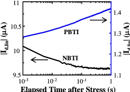
Fig. 2 shows the evolutions of NBT stress induced linear drain current change (ΔId,lin) in control SiO2 and HfSiON pMOSFETs by using the fast transient measurement system. The device dimension is W/L=10μm/0.2μm. The stress Vg is -2.8V, and the linear drain current (Id,lin) is measured at Vg/Vd= -1.2V/-0.2V. As shown in the figure, ΔId,lin decreases monotonically with stress time in a SiO2 control device, while a turn-around characteristic of ΔId,lin versus stress time is obtained in a HfSiON MOSFET. Note that one may fail to observe this anomalous turn-around behavior by using a conventional measurement setup such as Agilent 4156 due to a switching delay. Furthermore, the NBTI and its counterpart PBTI in a nMOSFET are compared in Fig. 3. The ΔId,lin in a nMOSFET (PBTI) is negative in the entire stress period and no turn-around feature like the NBTI is observed. More interestingly, the NBTI and the PBTI in HfSiON MOSFETs exhibit distinctly different post-stress drain current evolutions (Fig. 4). The PBTI exhibits a drain current recovery, as reported in literature [4]. However, the NBTI shows persistent drain current degradation after stress. The post-stress Id,lin degradation in a high-k pMOSFET implies trapped electron emission from a high-k gate dielectric after stressing Vg is removed. In Fig. 5 (a) and (b), NBT induced ΔId,lin at various stress Vg and temperatures are shown. The stress Vg ranges from -1.6V (result not shown in Fig. 5) to -2.8V with all other terminals grounded and the
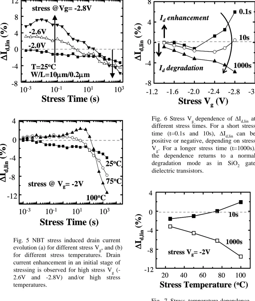
temperature is from 25°C to 125°C. For a stress Vg weaker than -2V (selectively shown for clarity), ΔId,lin is negative (degradation mode) and decreases monotonically with stress time. The degradation aggravates with a larger stress |Vg| (more negative). For a stress Vg stronger than -2V or a higher stress temperature, the drain current instability shows a different feature. The Id,lin initially increases with stress time (enhancement mode) and shortly evolves into degradation mode (ΔId,lin<0), featuring a turn-around characteristic in Fig. 5 (a) and (b). The drain current enhancement has a positive dependence on stress |Vg| and temperature. The transition time for the Id,lin evolving from enhancement mode to degradation mode is mostly within seconds in the bias range of interest. Fig. 6 demonstrates the dependence of ΔId,lin on stress Vg at different stress times. For t=0.1s, a lower stress |Vg| (-1.4V~ -2V) induces a Id,lin degradation while a larger stress |Vg| results in an enhancement. This trend remains for t=10s, but the turn-around |Vg| is slightly increased. For a longer stress time (e.g., t=1000s), the dependence of ΔId,lin on Vg returns to a normal degradation mode as in SiO2 gate dielectric transistors, and a larger stress |Vg| results in a larger degradation [8,9]. The stress temperature dependence of ΔId,lin is shown in Fig. 7. For a short stress time (e.g., t=10s), ΔId,lin changes from negative at low temperatures to positive at high temperatures. But for a longer stress time (e.g., t=1000s), the Id,lin degradation increases monotonically with stress temperature. The positive temperature dependence of the Id,lin degradation in a high-k MOSFET can be realized due to temperature accelerated
high-k/IL trap generation because of thermo-chemical reaction [10].
III. Bipolar Charge Trapping Model In a negative Vg stress, two carrier injection processes affect Id instability, (i) valence band electron injection from the p+ poly-gate into high-k traps (Id enhancement mode) and (ii) hole injection from the inverted channel into high-k/IL traps (Id degradation mode). Thus, available trap states in a high-k dielectric, either pre-existing traps or stress generated traps, and injected carrier fluence should be considered in a NBT instability model. Fig. 8 illustrates the energy band diagrams in equilibrium (Fig. 8(a)) and in various NBT stress conditions, for example, low Vg and low temperature stress (Fig. 8(b)), low Vg and high temperature stress (Fig. 8(c)), and high Vg and low temperature stress (Fig. 8(d)). In thermal equilibrium, trap states with energy (Et) below the Fermi level (EF) are occupied by electrons while those above EF are empty. The shaded area in Fig. 8 represents the occupied states in the high-k layer. When a low stress |Vg|/ temperature is applied (Fig. 8(b)), the empty high-k traps available for poly-gate valence electron injection are very limited due to a small band-bending ( Et) in a high-k gate dielectric. In this case, electron trapping into the high-k layer is negligible, and Id,lin is dominated by hole injection from the inverted channel, leading to a Id,lin degradation. In this regime, a larger |Vg| aggravates Id,lin due to a larger hole injection current, which is in agreement with our measured result in Fig. 6. As stress temperature or |Vg| increases, more poly-gate electrons can inject into pre-existing high-k traps either because of thermally assisted tunneling (Fig.8(c)) or because of more available
empty states due to a larger band-bending (Fig.8(d)). In these stress conditions, both electron trapping and hole trapping into the high-k layer are possible. The measurement result in Fig. 5(a) and (b) implies that electron trapping is dominant in the initial stress period and hole trapping gradually supersedes electron trapping due to new hole trap creation in the high-k and IL layers, thus resulting in a turn-around feature of the Id,lin evolution.
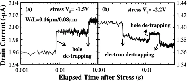
To confirm our bipolar charge trapping model for NBT instability, post-stress trapped charge emissions are characterized. The purpose of this characterization is to identify injected charge species during stress. The detail of this method was described in our previous papers for trapped electron emission from HfSiON in a nMOSFET [4] and trapped hole emission from SiO2 in a pMOSFET [11]. Fig. 9 shows our measured Id evolution patterns after low (-1.5V) and high (-2.2V) Vg stress, respectively. The transistors have W/L=0.16 m/0.08 m. The stress time (or exactly the charge filling time) for both cases is 0.2s, and the post-stress measurement condition is Vg~Vt and Vd=-0.2V. In Fig. 9, trapped charge emission is manifested by a staircase-like jump in the drain current. For a pMOSFET, an upward shift (increase in |Id|) corresponds to a single hole emission, and a downward shift corresponds to a single electron emission. Notably, only trapped hole emissions are found for the low Vg stress (Fig. 9(a)) while both electron and hole emissions are obtained for the high Vg stress (Fig. 9(b)). This single charge emission result provides direct evidence of bipolar charge trapping in a high Vg stress condition. It should be remarked that we did not observe any random telegraph signal at the
post-stress measurement biases, indicating that the observed current jumps in Fig. 9 are attributed to injected charge emissions.
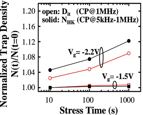
We also characterize high-k/IL trap generation for low and high Vg stress by using a charge pumping method. A two-frequency (5kHz and 1MHz) technique is used to separate IL/Si interface traps (Dit) from bulk high-k traps (NHK) [12]. The high frequency CP current is contributed by Dit and the difference between the CP currents of the two frequencies reflects high-k trap density NHK. Fig. 10 shows the extracted Dit and NHK versus stress time for stress Vg=-1.5V and -2.2V. No new traps are created in a low Vg (-1.5V) stress even for a stress time of t=1000s, indicating that the Id,lin degradation at a low stress Vg is mainly attributed to hole trapping into pre-existing high-k traps. On the other side, both interface trap and bulk high-k trap generation is observed in a high Vg (-2.2V) stress.
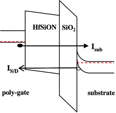
In addition to available traps for electron and hole injection, another factor affecting NBT instability mode is the fluence of injected carriers during stress. A carrier separation measurement was performed to explore the effect of injected carrier fluence on Id instability. Fig. 11 illustrates the carrier flow in a high-k pMOSFET under –Vg stressing. The hole injection current from the inverted channel constitutes the source/drain current (i.e., IS/D) and the electron injection current from the p+ poly-gate flows to the substrate (i.e., Isub). Fig. 12(a) shows the measured hole and electron currents versus stress gate voltage at T=25°C. Two points are worth noting; (i) Holes are the dominant conduction carrier at a low stress |Vg|. As a stress |Vg| increases, an electron current
becomes dominant. Thus, electron filling effect is more significant than hole filling at a higher stress |Vg|. This trend is consistent with the measured result in Fig. 6, i.e, Id,lin degradation in a low Vg region and Id,lin enhancement in a high Vg region in the initial stress period.
As stress temperature increases to 100°C (Fig. 12 (b)), the electron current is enhanced to a larger extent, compared to the hole current and thus it supersedes the hole current at a smaller stress Vg. This result is in agreement with our thermally-assisted electron tunneling model in Fig. 8(c) and can well explain the increased Id,lin enhancement at a higher temperature in a low stress Vg region (Fig. 5(b)).
IV. Conclusion
In this work, various NBT induced drain current instability modes in HfSiON pMOSFETs are investigated. The drain current enhancement is observed in the initial stress period in certain stress conditions. Electron trapping, hole trapping and new trap generation are found to be responsible for the drain current instability modes. The impact of stress Vg, temperature and stress time on NBT instability is characterized. In high |Vg| and/or high temperature stress, electron trapping into pre-existing high-k traps is dominant in the initial stress period, thus causing an Id enhancement. As stress continues, hole injection and new hole trap creation in HK/IL layers eventually become dominant, giving rise to a turn-around characteristic of the drain current evolution with time. For low Vg stress, the Id instability is dictated by hole injection throughout the entire stress period
References
[1] S. Zafar, B. H. Lee, J. Stathis, A. Callegari, and T. Ning, “A model for negative bias temperature instability (NBTI) in oxide and high k pFETs,” VLSI Tech. Dig. pp. 208-209, 2004 [2] M. Houssa, S. De Gendt, J. L. Autran, G. Groeseneken, and M. H. Heyns, “Detrimental impact of hydrogen on negative bias temperature instability in HfO2-based pMOSFETs,” VLSI
Tech. Dig. pp. 212-213, 2004
[3] M. Houssa, M. Aoulaiche, S. Van Elshocht, S. De Gendt, G. Groeseneken, and M. M. Heyns, ”Impact of Hf content on negative bias temperature instabilities in HfSiON-based gate stacks,” Appl. Phys. Lett., vol. 86, pp. 173509, 2005
[4] T. Wang, C. T. Chan, C. J. Tang, C. W. Tsai, H. C.-H. Wang, M. H. Chi, and D. D. Tang, “A novel transient characterization technique to investigate trap properties in HfSiON Gate Dielectric MOSFETs – from single electron emission to PBTI recovery transient,” IEEE
Trans. on Elec. Dev., vol. 53, pp. 1073-1079,
2006
[5] C. T. Chan, C. J. Tang, T. Wang, H. C.-H. Wang, and D. D. Tang, “Positive bias and temperature stress induced two-stage drain current degradation in HfSiON nMOSFET’s,”
IEDM Tech. Dig., pp. 571-574, 2005
[6] H.C.-H. Wang, S.-J. Chen, M.-F. Wang, P.-Y. Tsai, C.-W. Tsai, T.-W. Wang, S.M. Ting, T.-H. Hou, P.-S. Lim, H.-J. Lin, Y. Jin, H.-J. Tao, S.-C. Chen, C.H. Diaz, M.-S. Liang, and C. Hu, “Low power device technology with SiGe channel, HfSiON, and poly-Si gate,” IEDM Tech.
[7] H.C.-H. Wang, C. W. Tsai, S. J. Chen, C. T. Chan, H. J. Lin, Y. Jin, H. J. Tao, S. C. Chen, C. H. Diaz, T. Ong, A. S. Oates, M. S. Liang, and M. H. Chi, “Reliability of HfSiON as gate dielectric for advanced CMOS technology,”
VLSI Tech. Dig. pp. 170-171, 2005
[8] N. Kimizuka, T. Yamamoto, T. Mogami, K. Yamaguchi, K. Imai, and T. Horiuchi, “The impact of bias temperature instability for direct-tunneling ultra-thin gate oxide on MOSFET scaling,” VLSI Tech. Dig. pp. 73-74, 1999
[9] S. Mahapatra, P. Pharath Kumar, and M. A. Alam, “Investigation and modeling of interface and bulk trap generation during negative bias temperature instability in p-MOSFETs,” IEEE
Trans. on Elec. Dev., vol. 51, pp. 1371-1379,
2004
[10] T. Yamaguchi, I. Hirano, R. Iijima, K. Sekine, M. Takayanagi, K. Eguchi, Y. Mitani, and N. Fukushima, “Thermochemical understanding of dielectric breakdown in HfSiON with current acceleration,” Proc. Int.
Reliab. Phys. Symp., pp. 67-74, 2005
[11] C. T. Chan, H. C. Ma, C. J. Tang, and T. Wang, “Investigation of post-NBTI stress recovery in pMOSFETs by direct measurement of single oxide charge de-trapping,” VLSI Tech.
Dig. pp. 90-91, 2005
[12] R. Degraeve, A. Kerber, P. Roussell, E. Cartier, T. Kauerauf, L. Pantisano, G. Groeseneken, “Effect of bulk trap density on HfO2 reliability and yield,” IEDM Tech. Dig., pp. 935-938, 2003
Digital Osc. OpAmp R Stress Meas. Stress Stress Meas. Meas. G D S Digital Osc. OpAmp R Stress Meas. Stress Stress Meas. Meas. G D S
-8
Δ
I
d, lin(%
)
-4
12
8
4
0
Stress Time (s)
10
-310
-110
110
3HfSiON
pMOS
SiO
2pMOS
-8
Δ
I
d, lin(%
)
-4
12
8
4
0
Stress Time (s)
10
-310
-110
110
3HfSiON
pMOS
SiO
2pMOS
Fig. 1 Schematic diagram for the transient measurement system. The high speed switches minimize a switching delay down to microseconds between stress and drain current measurement.
Fig. 2 NBT stress induced linear drain current change (ΔId,lin) in SiO2 and HfSiON pMOSFETs. The stress Vg is -2.8V and the linear drain current (Id,lin) is measured at Vg/Vd=-1.2V/-0.2V.
8
0
-8
4
-12
T=25
oC
Δ
I
d, li n(%
)
10
-310
-110
3Stress Time (s)
10
112
-4
NBTI
PBTI
HfSiON MOSFETs
8
0
-8
4
-12
T=25
oC
Δ
I
d, li n(%
)
10
-310
-110
3Stress Time (s)
10
112
-4
NBTI
PBTI
HfSiON MOSFETs
Fig. 3 Linear drain current change (ΔId,lin) in a pMOSFET (NBTI) and in a nMOSFET (PBTI). The stress Vg is -2.8V for the pMOSFET and 2.2V for the nMOSFET.
10-3 10-2 1
Elapsed Time after Stress (s)
10-1 11 10.5 10 9.5 1.1 1.3 1.4 1.2
|I
d, li n| (
μA)
NBTI PBTI|I
d, li n| (
μA)
10-3 10-2 1Elapsed Time after Stress (s)
10-1 11 10.5 10 9.5 1.1 1.3 1.4 1.2
|I
d, li n| (
μA)
NBTI PBTI|I
d, li n| (
μA)
Fig. 4 |Id,lin| as a function of elapsed time after stress. The drain current recovery is observed in a nMOSFET, while the NBTI shows persistent post-stress current degradation.
Stress Time (s)
-8
0
4
8
12
Δ
I
d, lin(%
)
-4
10
-310
-110
110
3T=25
oC
-2.0V
-2.6V
stress @Vg= -2.8V
W/L=10
μm/0.2μm
Stress Time (s)
-8
0
4
8
12
Δ
I
d, lin(%
)
-4
10
-310
-110
110
3T=25
oC
-2.0V
-2.6V
stress @Vg= -2.8V
W/L=10
μm/0.2μm
-12
-4
0
4
Δ
I
d, lin(%
)
-8
10
-310
-110
110
3stress @ V
g= -2V
25
oC
100
oC
75
oC
Stress Time (s)
-12
-4
0
4
Δ
I
d, lin(%
)
-8
10
-310
-110
110
3stress @ V
g= -2V
25
oC
100
oC
75
oC
Stress Time (s)
Fig. 5 ΝΒΤ stress induced drain current evolution (a) for different stress Vg, and (b) for different stress temperatures. Drain current enhancement in an initial stage of stressing is observed for high stress Vg (-2.6V and -2.8V) and/or high stress temperatures.
0.1s
10s
1000s
-8
0
4
8
Δ
I
d, li n(%
)
-4
Stress V
g(V)
-1.2
-1.6
-2.0
-2.4
-2.8
-3.2
I
denhancement
I
ddegradation
0.1s
10s
1000s
-8
0
4
8
Δ
I
d, li n(%
)
-4
Stress V
g(V)
-1.2
-1.6
-2.0
-2.4
-2.8
-3.2
I
denhancement
I
ddegradation
Fig. 6 Stress Vg dependence of ΔId,lin at different stress times. For a short stress time (t=0.1s and 10s), ΔId,lin can be positive or negative, depending on stress Vg. For a longer stress time (t=1000s), the dependence returns to a normal degradation mode as in SiO2 gate dielectric transistors.
-12
-4
0
4
Δ
I
d,lin(%
)
-8
Stress Temperature (
oC)
100
40
20
60
80
10s
1000s
stress V
g= -2V
-12
-4
0
4
Δ
I
d,lin(%
)
-8
Stress Temperature (
oC)
100
40
20
60
80
10s
1000s
stress V
g= -2V
Fig. 7 Stress temperature dependence of ΔId,lin.
E
FpE
FnΔE
t(b)
(a)
ΔE
t(d)
ΔE
t(c)
thermally-assisted tunnelingthermal equilibrium
(pre-stress)
low |V
g| / low T stress
high T / low |V
g| stress
high |V
g| / low T stress
HK IL Si
E
F poly-gateE
FpE
FnΔE
t(b)
(a)
ΔE
t(d)
ΔE
t(c)
thermally-assisted tunnelingthermal equilibrium
(pre-stress)
low |V
g| / low T stress
high T / low |V
g| stress
high |V
g| / low T stress
HK IL Si
E
Fpoly-gate
Fig. 8 Schematic representation of an energy band diagram and charge injection processes in (a) thermal equilibrium, (b) low |Vg|/ low T stress, (c) high T/ low |Vg| stress, and (d) high |Vg|/ low T stress. The shaded area represents the occupied trap states in the high-k layer. Electron injection from the poly gate and hole injection from the channel are illustrated.
Drai
n C
u
rren
t
(-μA)
0.001 0.01 1.94 1.96 1.98 2.00 2.02 2.04 (a) stress Vg= -1.5V W/L=0.16μm/0.08μm hole de-trapping 0.001 0.01 1.34 1.36 1.38 1.40 1.42 1.44 (b) stress Vg= -2.2V hole de-trapping electron de-trappingElapsed Time after Stress (s)
Drai
n C
u
rren
t
(-μA)
0.001 0.01 1.94 1.96 1.98 2.00 2.02 2.04 (a) stress Vg= -1.5V W/L=0.16μm/0.08μm hole de-trapping 0.001 0.01 1.34 1.36 1.38 1.40 1.42 1.44 (b) stress Vg= -2.2V hole de-trapping electron de-trappingElapsed Time after Stress (s)
Fig. 9 Post-stress Idevolution patterns in small-area devices after (a) a low |Vg| (-1.5V) stress and (b) a high |Vg| (-2.2V) stress. The post-stress measurement condition is Vg~Vtand Vd=-0.2V.
Stress Time (s)
10
100
1000
N
o
rm
a
li
zed T
rap D
ens
it
y
N(
t)
/N(
t=
0
)
1.20
1.16
1.04
open: D
it(CP@1MHz)
solid: N
HK(CP@5kHz-1MHz)
V
g= -1.5V
V
g= -2.2V
1.08
1.12
1.00
Stress Time (s)
10
100
1000
N
o
rm
a
li
zed T
rap D
ens
it
y
N(
t)
/N(
t=
0
)
1.20
1.16
1.04
open: D
it(CP@1MHz)
solid: N
HK(CP@5kHz-1MHz)
V
g= -1.5V
V
g= -2.2V
1.08
1.12
1.00
Fig. 11 Interface traps (Dit) and bulk high-k traps (NHK) growth rates in NBT stress at Vg=-1.5V and Vg=-2.2V. A two-frequency charge pumping method is used.
C
hannel Current
(
μA)
0.92
0.96
Elapsed Time after Stress (s)
10
-3 pre-stress post-stress recovery W/L=0.16μm/0.08μm10
-210
-110
01.00
1.04
1.08
0.88
C
hannel Current
(
μA)
0.92
0.96
Elapsed Time after Stress (s)
10
-3 pre-stress post-stress recovery W/L=0.16μm/0.08μm10
-210
-110
01.00
1.04
1.08
0.88
Fig. 10 Poststress Id evolution patterns after stress at Vg = 0.7 V for 0.2 s in an nMOSFET. The poststress measurement condition is Vg/Vd =0.3 V/0.2 V.
I
S/DHfSiON SiO
2I
subsubstrate
poly-gate
I
S/DHfSiON SiO
2I
subsubstrate
poly-gate
T=25oC Jsub(e) JS/D(h) 0 -0.5 -1 -1.5 -2 -2.5 -3Gate Voltage (V)
10 1 10-1 10-2 10-3Current D
en
sit
y
(A
/c
m
2)
T=25oC Jsub(e) JS/D(h) 0 -0.5 -1 -1.5 -2 -2.5 -3Gate Voltage (V)
10 1 10-1 10-2 10-3Current D
en
sit
y
(A
/c
m
2)
Fig. 12 Illustration of carrier flow in a high-k pMOSFET under –Vg stressing. Isub denotes the electron injection current from the p+ poly-gate to substrate, and IS/Dstands for hole injection current from the inverted channel.
T=100oC Jsub(e) JS/D(h) 0 -0.5 -1 -1.5 -2 -2.5 -3
Gate Voltage (V)
10 1 10-1 10-2 10-3C
u
rren
t D
en
sity
(A
/c
m
2)
T=100oC Jsub(e) JS/D(h) 0 -0.5 -1 -1.5 -2 -2.5 -3Gate Voltage (V)
10 1 10-1 10-2 10-3C
u
rren
t D
en
sity
(A
/c
m
2)
Fig. 13 Gate voltage dependence of hole injection current (IS/D) and electron injection current (Isub) in a high-k pMOSFET, measured at (a) T=25°C and (b) T=100°C.