Characterization of environment-dependent hysteresis in indium gallium zinc oxide
thin
film transistors
Yu-Chun Chen
a, Ting-Chang Chang
a,b,⁎
, Hung-Wei Li
c, Wan-Fang Chung
d, Shih-Cheng Chen
e,
Chang-Pei Wu
a, Yi-Hsien Chen
a, Ya-Hsiang Tai
f, Tseung-Yuen Tseng
d, Fon-Shan Yeh(Huang)
ea
Department of Physics, National Sun Yat-Sen University, Kaohsiung, Taiwan, ROC
b
Center for Nanoscience & Nanotechnology, National Sun Yat-Sen University, Kaohsiung, Taiwan, ROC
c
Department of Photonics & Institute of Electro-Optical Engineering, National Chiao Tung University, Hsinchu, Taiwan, ROC
d
Department of Electronics Engineering & Institute of Electronics, National Chiao Tung University, Hsinchu, Taiwan, ROC
eDepartment of Electrical Engineering & Institute of Electronic Engineering, National Tsing Hua University, Taiwan, ROC f
Department of Photonics & Display Institute, National Chiao Tung University, Hsinchu, Taiwan, ROC
a b s t r a c t
a r t i c l e i n f o
Available online 7 March 2012 Keyword:
Indium gallium zinc oxide Thinfilm transistors Hysteresis
This study investigates environmentally dependent electrical performance as a function of hysteresis phe-nomena for amorphous indium–gallium–zinc-oxide (a-IGZO) thin film transistors (TFTs). Because ambient gas has a great influence on the electrical characteristics of zinc oxide-based TFTs during electrical measure-ments, the hysteresis for current–voltage and capacitance–voltage measurements are employed in different ambient gases (ambient air, vacuum, oxygen ambient and moisture ambient) to study this issue. Although the hysteresis phenomenon has been explained by the charge trapping and de-trapping model, in order to obtain stable electrical characteristics it is necessary to clarify the original principal mechanism leading to threshold voltage instability under gate bias operations in different environments. Also, the relationship be-tween de-trapping rate and electrical hysteresis is investigated by prolonging the integration time of the semiconductor parameter analyzer. This study may be of importance in explaining the dynamic relationship between the TFT electrical characteristics and ambient gas, as well as providing a better understanding of the environment-dependent hysteresis phenomenon of the IGZO TFTs.
© 2012 Elsevier B.V. All rights reserved.
1. Introduction
Recently, amorphous oxide semiconductors (AOSs) have been considered appropriate for application in thinfilm transistors (TFTs) for use in large-areaflexible electronic devices due to the great elec-trical uniformity and process advantage of being deposited at room temperature [1–4]. Compared to hydrogenated amorphous silicon (a-Si:H), they have excellent electron mobility and a reduced density of band tail state because their conduction band is composed of spherical overlapping orbital[5]. In particular, ZnO-based semicon-ductors incorporate indium-oxide and gallium-oxide or hafnium-oxide as a carrier mobility enhancer and as a structure suppressor for amorphous phase, respectively, to achieve channel material re-quirements of highfield effect mobility and low leakage current, such as In–Ga–Zn–O and Hf–In–Zn–O[6–8]. Moreover, due to the high carrier mobility of AOSs, transparent andflexible nonvolatile memories can be developed by incorporating AOSs, in order to meet the future goals of system-on-panel applications[9,10]. In previous
studies, the ambient gas causes a notable reliability on the electrical characteristic of ZnO-based TFTs under a gate bias stress[11–14]. Al-though some proper passivation layers to eliminate the influence of ambient gas on the active layer have been studied[15–17], it is advis-able to establish the principal ambient-induced mechanism which can be expected to decrease any environment ambient effects with-out a passivation layer and therefore reduce panel cost. However, very little research has focused on the electrical hysteresis phenome-na of a-IGZO TFT under rapid on-state or off-state operation in actual display applications[18].
2. Experiment detail 2.1. TFT fabrication
In this article, we investigate the environmental effect on the elec-trical hysteresis by current–voltage (I–V) and capacitance–voltage (C–V) measurements. For this purpose, passivation-free bottom gate coplanar a-IGZO TFTs are adopted to examine the electrical hysteresis of a-IGZO TFTs in different ambient gases. First, the patterned Ti/Al/Ti (50/200/50 nm) tri-layer gate electrodes on glass substrate were capped with SiOx (300 nm)film as gate insulator, which was grown
Surface & Coatings Technology 231 (2013) 531–534
⁎ Corresponding author at: Department of Physics, National Sun Yat-Sen University, Kaohsiung, Taiwan, ROC.
E-mail address:[email protected](T.-C. Chang). 0257-8972/$– see front matter © 2012 Elsevier B.V. All rights reserved. doi:10.1016/j.surfcoat.2012.02.057
Contents lists available atScienceDirect
Surface & Coatings Technology
j o u r n a l h o m e p a g e : w w w . e l s e v i e r . c o m / l o c a t e / s u r f c o a tby plasma enhanced chemical vapor deposition (PECVD) at 370 °C. The source/drain electrodes were formed by DC sputtering with Ti/ Al/Ti (50/200/50 nm) and then patterned by wet-etching. The active layer, composed of 30 nm thick a-IGZO, was deposited by DC magne-tron sputtering system at room temperature, using a target of In:Ga: Zn = 1:1:1 in atomic ratio. The process was performed with a plasma discharge power of 300 W, and in a 5 mTorr (0.6 Pa) working pres-sure of argon ambiance with oxygen partial prespres-sure ratio of 6.7%. The patterned dimensions of the channel are 10–15 μm in width and 10μm in length. Finally, all of the devices were annealed in an oven in an ambient air at 330 °C for 2 h in an O2gas with the H2O
par-tial pressure ratio of 19.7%. 2.2. TFT characterization
The I–V and C–V characteristics of a-IGZO TFTs were measured at room temperature by an Agilent B1500 semiconductor parameter an-alyzer. The probe station is set in a vacuum chamber with gasflow control and moisture feeding equipment[19]. All of the electrical op-erations under different ambient gas were performed in the dark at room temperature. The VTwas determined by using the constant
cur-rent method as the gate voltage which induces a drain curcur-rent of L/ W × 1 nA, and subthreshold swing (SS) is determined by the equation SS = dVGS/ d(log IDS) (V/dec) while the current is between 10− 10and
10− 9A. For the C–V measurement, the VTwas extracted by the gate
voltage (VGS) which induced 1/3 of maximum capacitance.
3. Experiment result and discussions
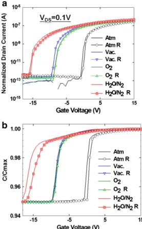
Fig. 1(a) shows the electrical hysteresis of source-to-drain current (IDS) as a function of VGSwith thefixed drain voltage (VDS) at 0.1 V in
linear regime of a-IGZO TFTs under different environments of ambi-ent air, 1 × 10− 4Torr vacuum, H2O/N2 (moisture ambient), and
oxygen ambient. The VGSis swept by 0.75 V increments along a
for-ward sweep from a negative voltage to a positive voltage, and along a reverse sweep from positive voltage back to the starting negative voltage (e.g.,−30 to 30 to −30 V). Clockwise hysteresis of transfer curves with different VTbetween forward sweep and reverse sweep
are observed in different ambiences. Recently, a-IGZO TFTs have been shown to be basically n-type devices with a positive bias gener-ating an accumulation layer of electrons in a channel close to the channel/dielectric interface[7]. The electrical hysteresis phenomenon has been explained by the variations of interface state occupancy be-tween the insulator and channel in a-Si:H TFTs[20]. Our experiment results showed clear hysteresis in atmosphere and moisture ambient but minimal hysteresis in vacuum for the same device, indicating that the charge trapping model cannot entirely explain the hysteresis be-havior, as shown inFig. 1(a). Meanwhile, the estimated SS value dif-ferences between forward sweep and reverse sweep in atmospheric and moisture ambient are both about 0.2. This indicates that the in-terface states of a-IGZO TFTs were altered in ambient air and moisture ambient[19,21,22]. Thus, to investigate the various subgap states of the channel layer or the gate insulator (GI)/semiconductor interface characteristics in detail, electrical hysteresis in the C–V measurement at 100 kHz frequency with 0.75 V increment of gate voltage was per-formed and shown inFig. 1(b). Compared to the I–V measurement without any apparent change, the C–V measurement is more sensi-tive to the variation of the interface state of the device. It has been reported that environment effects such as bias-induced oxygen ad-sorption or metastable gap state induced by moisture could acceler-ate the instability of a-IGZO TFTs [14,19,24]. These phenomena imply that a complex mechanism causes the electrical hysteresis in ambient air, as will be discussed later.
Fig. 2shows the I–V and C–V hysteresis of the a-IGZO TFTs mea-sured in a vacuum environment. Clearly, no abnormality between the forward sweep and reverse sweep both in the I–V and C–V hyster-esis measurements can be observed. In general, because of the ab-sence of ambient gas, this result has been suggested to be due to electron trapping in the preexisting traps located at the GI/semicon-ductor interface. Note that the interface-trapped electron interrupts the subsequentflow of electron in the channel layer. As a result, even the stop sweep VGSwas doubled from 15 V to 30 V, and no I–V
hysteresis was found, which clarifies that no more electron traps exist at the GI/ a-IGZO interface. Literature has implied that the band tail state generated from structural disorder and defects may be eliminated by incorporating hydrogen into a-IGZO during active layer deposition or thermal annealing at the end of the fabrication process.[5,25]
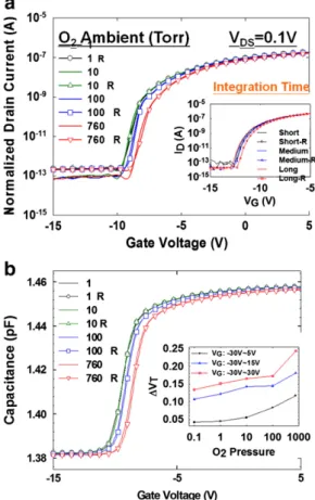
InFig. 3(a) and (b), the I–V and C–V hysteresis measurement are shown for a-IGZO TFTs in oxygen ambient pressures of 1 Torr, 10 Torr, 100 Torr and 760 Torr, respectively. The SS of the forward and reverse sweeps are similar, exhibiting no defect creation at the
Fig. 1. Electrical hysteresis of (a) IDs–VGscharacteristics withfixed drain voltage (VDS)
at 0.1 V and (b) C–V characteristics of a-IGZO TFTs in linear regime for a-IGZO TFTs under ambient air, vacuum, moisture ambient, and oxygen ambient.
Fig. 2. I–V and C–V hysteresis characteristics of a-IGZO TFTs measured with different gate sweep ranges in vacuum environment.
GI/semiconductor interface under different oxygen partial pressures. In the inset ofFig. 3(a), the estimated delta VTfrom I–V hysteresis
of a-IGZO TFT increases with increasing oxygen partial pressure. These results indicate that two responsible mechanisms for the delta VTcan be proposed: (1) simple charge trapping phenomenon
and (2) environment effects. Moreover, the same tendency of the C–V hysteresis measurement without any distortion was observed inFig. 3(b). The delta VTof the C–V hysteresis measurement in
oxy-gen ambient with different ending of positive sweep VGSis depicted
in the inset ofFig. 3(b). The experimental results inFig. 3(b) demon-strate that the more oxygen that surrounds a-IGZO TFTs, the more delta threshold voltage is measured. A previous study suggested that the surrounding oxygen molecules can capture electrons from the conduction band and then adsorb on the device as a form of O2+ e−→O2−(ads), resulting in a depletion layer in the active
back-channel[23]. If the electron trapping/de-trapping mechanism domi-nates the hysteresis phenomenon of a-IGZO TFTs in oxygen ambient by prolonging the measurement integration time, the de-trapping rate would be enhanced and electrical hysteresis would be reduced
[20]. Because the de-trapping rate increases with longer integration time, the electron released from trapping states helps the current flow in the reverse sweep, so a smaller positive shift of reverse sweep curve would be observed.
The inset ofFig. 3(a) represents the I–V hysteresis of a-IGZO TFT with short (20 ms), medium (40 ms) and long (2 s) integration times. For the long time, the reverse sweep shows a clear increase of VT in the inset of Fig. 3(a), which seems to be different from
those found in previous work[20]. Even the oxygen in ambient and the interface trap act in the same role to trap electrons and cause an increase in VT; nevertheless, the de-trapping time of chemisorbed
electrons from oxygen is longer than interface trapped electron. Thus, this phenomenon may be associated with more bias-induced adsorption oxygen on the back channel of a-IGZO TFTs during the on-state period. We assume that during forward measurement, one oxygen molecule in environment can capture an electron from the conduction band during large electrical currentflow in the channel layer. A schematic of the possible mechanism during rapid operation in oxygen ambient is depicted inFig. 4(a). With increasing VGS, the
bent energy band of a-IGZO causes the chemisorption of oxygen which lowers the Fermi level. During the reverse sweep, in
Fig. 4(b), the oxygen chemisorbed on the back channel of a-IGZO TFTs screens the applied gate voltage, which produces a lower VGS
re-quired to turn off the a-IGZO TFTs during reverse sweep. Therefore, the more time during the on state, the more chemisorption of oxygen occurs, as shown in the inset ofFig. 3(b).
Fig. 1(a) and (b) shows about−14 V VTshift, a 0.5 degradation in
SS for the I–V curve and a distorted C–V curve for the device in mois-ture ambient when compared to atmosphere ambient. This implies that the creation of subgap states in a-IGZO arise from the moisture ambient[21–23]. For the hysteresis C–V measurement inFig. 1(b), it can be assumed that the creation states in the GI/channel layer in-terface screen the applied gate voltage in moisture ambient, leading to a C–V measurement that is largely stretched out. It should be noted that the distorted C–V of a pristine device is particularly ranged in a gate voltage regime that corresponds to the off-state in the I–V measurement. In order to investigate the cause of this phenomenon, we measured the hysteresis C–V characteristics by two different gate voltage sweep ranges. One is from off state to close to the
on-Fig. 3. The evolution of (a) IDs–VGsand (b) C–V hysteresis measurement for a-IGZO TFTs
in oxygen ambient pressures of 1 Torr, 10 Torr, 100 Torr and 760 Torr. The inset of fig-ure (a) shows the I–V hysteresis measfig-urement with different integration times. The inset offigure (b) shows the delta threshold voltage of C–V hysteresis measurement with different VG sweep ranges in oxygen ambient pressures of 1 Torr, 10 Torr,
100 Torr and 760 Torr.
Fig. 4. Schematic band diagram explaining the experiment result, which are (a) chem-isorption of oxygen with increasing VGduring the on-state of a-IGZO TFTs (b)
chemi-sorbed oxygen on the back channel of a-IGZO TFTs screen the applied VGduring the
reverse sweep.
Fig. 5. C–V hysteresis measurement with VGsweep range from−30 V to 15 V and VG
sweep range from−15 V to 30 V (inset) in the moisture ambient of pressures of 1 Torr, 10 Torr, 100 Torr and 760 Torr.
533 Y.-C. Chen et al. / Surface & Coatings Technology 231 (2013) 531–534
state (−30 V to 15 V), and the other is from subthreshold state to the on-state (−15 V to 30 V). InFig. 5, C–V curves which sweep range is from off state to on-state are stretched-out toward the negative direction as environmental moisture increases. In literature, the chemisorption of moisture molecules seems to act as a donor-like trap in a-IGZO[26]. Nev-ertheless, Nomura et al. reported a high density of occupied sub gap states near the valence band maximum in a-IGZO[5]. However, the inset ofFig. 5demonstrates that the significant on-state degradation in the C–V measurement can be attributed to the generation of acceptor-like traps by the adsorption of moisture on the shallow traps in a-IGZO. The VTshift by this interface charge increases as the gate voltage sweeps
toward the positive direction, indicating that they are negative when traps are occupied by electrons, as acceptor-like states. We assume that the adsorption of moisture is uniform in the channel layer by reaction as a form of H2O +M\O\M→M\OH+M\OH+Vo++e−, where M
is the metal cation and Vo+is the oxygen vacancy. The O-vacancies of
ZnO-based semiconductors are easily hydroxylated due to residual water[27,28]. Hence, in this case, it is possible that the acceptor-like traps and donor-like traps are generated in an a-IGZO channel layer due to the adsorption of moisture molecules.[26]
InFig. 6, as the sweeping gate voltage becomes more positive, the positive shift of VTin the reverse C–V measurement occurs, which
re-sults in a decreasing magnitude of capacitance for the same applied gate voltage. In general, the total capacitance can be ascribed to the product of the total balance charge and VGS. The balance charge can
be expressed as the sum of a-IGZO charge (QS) and interface trapping
charge (QI), while the QSis constant under the same VGSin the
for-ward sweep. Thus, the delta capacitance in hysteresis C–V measure-ment is induced by electron trapping in the defect states created from adsorption of moisture. For a higher positive starting gate volt-age in the reverse voltvolt-age sweeps, since the Fermi-level is nearer to the conduction band, many acceptor-like traps arefilled, resulting in an increasing hysteresis C–V phenomenon.
4. Conclusions
In summary, the electrical hysteresis phenomenon of a-IGZO TFTs is analyzed in different environments by I–V and C–V measurement. In oxygen ambient, the parallel shift between forward sweep and re-verse sweep from the I–V or C–V characteristics of a-IGZO TFTs can be thought of as the chemisorption of oxygen for increasing VGduring
the on-state. On the contrary, the hydroxylated O-vacancies forming O\H species in a-IGZO are generated from dissociation of H2O
molecules in the environment, which causes more defect states in a-IGZO. Moreover, the created state from moisture increases the hys-teresis C–V phenomenon by accelerating the electron trapping rate. These results indicate that the electrical hysteresis phenomenon of a-IGZO TFTs in atmospheric ambient can be regarded as the combina-tion of the hysteresis characteristics in the oxygen ambient and mois-ture ambient.
Acknowledgment
This work was performed at National Science Council Core Facilities Laboratory for Nano-Science and Nano-Technology in Kaohsiung-Pingtung area. The authors would like to acknowledge thefinancial sup-port of the National Science Council of the Republic of China under con-tract no. NSC-100-2120-M-110-003.
References
[1] K. Nomura, H. Ohta, A. Takagi, T. Kamiya, M. Hirano, H. Hosono, Nature 432 (2004) 488.
[2] David Seo, Sanghun Jeon, Sunae Seo, Ihun Song, Appl. Phys. Lett. 97 (2010) 172106.
[3] Mandar J. Gadre, T.L. Alford, Appl. Phys. Lett. 99 (2011) 051901.
[4] Min-Chen Chen, Ting-Chang Chang, Sheng-Yao Huang, Hung-Wei Li, Appl. Phys. Lett. 94 (2009) 162111.
[5] Toshio Kamiya, Kenji Nomura, Hideo Hosono, J. Disp. Technol. 5 (2009) 273. [6] Chang-Jung Kim, Sangwook Kim, Je-Hun Lee, Jin-Seong Park, Appl. Phys. Lett. 95
(2009) 252103.
[7] Toshio Kamiya, Kenji Nomura, Hideo Hosono, Sci. Technol. Adv. Mater. 11 (2010) 044305.
[8] Wan-Fang Chung, Ting-Chang Chang, Hung-Wei Li, Shih-Ching Chen, Appl. Phys. Lett. 98 (2011) 152109.
[9] Huaxiang Yin, Sunil Kim, Chang Jung Kim, Ihun Song, Appl. Phys. Lett. 93 (2008) 172109.
[10] Min-Chen Chen, Ting-Chang Chang, Sheng-Yao Huang, Shih-Ching Chen, Electro-chem. Solid-State Lett. 13 (2010) H191.
[11] Jae Kyeong Jeong, Hui Won Yang, Jong Han Jeong, Yeon-Gon Mo, Appl. Phys. Lett. 93 (2008) 123508.
[12] Te-Chih Chen, Ting-Chang Chang, Chih-Tsung Tsai, Tien-Yu Hsieh, Appl. Phys. Lett. 97 (2010) 112104.
[13] M.E. Lopes, H.L. Gomes, M.C.R. Medeiros, P. Barquinha, Appl. Phys. Lett. 95 (2009) 063502.
[14] Yu-Chun Chen, Ting-Chang Chang, Hung-Wei Li, Shih-Ching Chen, Appl. Phys. Lett. 96 (2010) 262104.
[15] Shinhyuk Yang, Doo-Hee Cho, Min Ki Ryu, Sang-Hee Ko Park, Appl. Phys. Lett. 96 (2010) 213511.
[16] Sheng-Yao Huang, Ting-Chang Chang, Min-Chen Chen, Shih-Ching Chen, Electro-chem. Solid-State Lett. 14 (2011) H177.
[17] Te-Chih Chen, Ting-Chang Chang, Tien-Yu Hsieh, Chih-Tsung Tsai, Appl. Phys. Lett. 97 (2010) 192103.
[18] Te-Chih Chen, Ting-Chang Chang, Tien-Yu Hsieh, Wei-Siang Lu, Appl. Phys. Lett. 99 (2011) 022104.
[19] Kwang-Hee Lee, Ji Sim Jung, Kyoung Seok Son, Joon Seok Park, Appl. Phys. Lett. 95 (2009) 232106.
[20] Jae-Hoon Lee, Kwang-Sub Shin, Joong-Hyun Park, Min-Koo Han, J. Korean Phys. Soc. 48 (2006) s76.
[21] Jin-Seong Park, Jae Kyeong Jeong, Hyun-Joong Chung, Yeon-Gon Mo, Appl. Phys. Lett. 92 (2008) 072104.
[22] Wan-Fang Chung, Ting-Chang Chang, Hung-Wei Li, Chi-Wen Chen, Electrochem. Solid-State Lett. 14 (2010) H114.
[23] Y. Takahashi, M. Kanamori, A. Kondoh, H. Minoura, Jpn. J. Appl. Phys., Part 1 33 (1994) 6611.
[24] Wan-Fang Chung, Ting-Chang Chang, Hung-Wei Li, Shih-Ching Chen, Electro-chem. Solid-State Lett. 14 (6) (2011) H235.
[25] S.W. Tsao, Ting-Chang Chang, Sheng-Yao Huang, Min-Chen Chen, Solid State Elec-tron. 54 (2010) 1497.
[26] Himchan Oh, Sung-Min Yoon, Min Ki Ryu, Chi-Sun Hwang, Appl. Phys. Lett. 97 (2010) 183502.
[27] Kenji Nomura, Toshio Kamiya, Hiromichi Ohta, Masahiro Hirano, Hideo Hosono, Appl. Phys. Lett. 93 (2008) 192107.
[28] Olga Dulub, Bernd Meyer, Ulrike Diebold, Phys. Rev. Lett. 95 (2005) 136101. Fig. 6. C–V hysteresis measurement with different ending of positive gate voltages. The
inset shows the estimated delta VTfrom C–V hysteresis measurement for different
end-ing of positive gate voltages.