Study on the Second-Order Sustaining Driver for Plasma Display Panel
Chern-Lin Chen Shin-Tai Lo Cheng-Chang Liu Homg-Bin Hsu Kelvin Lee Department of Electrical Engineering Acer Display Technology
National Taiwan University Hsin-Chu, Taiwan
Abstract
The sustaining driver for plasma display panel (PDP) should provide alternating high voltage pulses to ignite plasma and recover the energy stored in the intrinsic capacitance between the scanning and sustaining electrodes inside the panel. Second-order circuits utilizing the series- connected or parallel-connected external inductance and intrinsic capacitance have been successfully adopted for the sustaining driver. In this way, high efficiency and low component count can be achieved. In this paper, the electrical characteristics of second-order drivers in the sustaining operation mode are investigated and influence of the ignited plasma discharging current on the driver performance is discussed.
141
I. Introduction
Plasma display panels which have the large view angle and potentially large screen dimensions take advantages over the other competing flat panel technologies and are expected to be the displays of the next generation. PDPs comprise a structure including a pair of substrates respectively supporting scanning, sustaining and addressing electrodes each coated with a dielectric layer. A desired color light display function is achieved by exciting those phosphors on the dielectric layer to emit visible light with the ultraviolet photons generated by the gas discharge.
PDPs are arrays of individually controllable electric discharges in short gaps [l] and its fimdamental driving operations are addressing and sustaining. In the addressing period, selective- write discharges can be initiated at given discharge cells by applying data pulses to the addressing electrodes and scanning pulses to the scanning electrodes at the same timings. Afterwards, the discharges at the selected cells can be continuously “sustained” between sustaining electrodes and adjacent scanning electrodes by applying alternating voltage pulses which themselves are insufficient to initiate a discharge. The intrinsic panel inter-electrode capacitance is formed because a dielectric layer exists between scanning and sustaining electrodes and there is unacceptably high power dissipation for large diagonal panels in the plasma display sustaining driver. With the view of high efficiency, not only should provide alternating voltage pulses to ignite plasma, the sustaining driver but also recovers the energy stored in the intrinsic panel capacitance.
In Section 11, two types of second-order sustaining drivers that utilize effects of series- resonance and parallel-resonance respectively are discussed. As a result of the electric breakdown of
the gas mixture when charging the intrinsic panel capacitance, the subsequent transient electric discharges causes an ignited plasma discharging current. In Section 111, a mathematical attempt is made to analyze the influence of the discharging current on the two types of second-order sustaining drivers.
11. Series-Resonance and Parallel-Resonance
Sustaining Drivers
To provide alternating sustaining voltage across the intrinsic panel capacitance, the plasma display sustaining driver generally includes a charging and discharging circuit and a voltage clamping circuit. The intrinsic panel capacitance is dependent on the panel size. Among different kinds of sustaining drivers, a voltage clamping circuit that adopts the full bridge configuration is usually utilized. The panel electrodes are connected between the two legs of the full bridge circuit. ‘The intrinsic panel capacitance is then charged and discharged through an inductor instead of through the lossy resistance of switches [2]. Two typical second-order sustaining drivers are respectively shown in Fig. 1 and Fig.2.
A. Series-Resonance Sustaining Driver [3]
The sustaining driver in Fig.1 comprises two independent charging and discharging circuits. One is on the scanning side and the other is on the sustaining side. Considering only the scanning side circuit, the intrinsic panel capacitance
c,
and the energy recovery capacitancecs
are series connected by an external inductor L and the sustaining driver utilizes the series resonance amongcP
, L , andcs
to charge or discharge the intrinsic panel capacitance. In other words, the energy discharged from the energy recovery capacitancecs
is used to charge the intrinsic panel capacitancecp
and the energy discharged142 ASID‘99
from the intrinsic panel capacitance
c,
can also be temporarily stored in the energy recovery capacitancec,.
Therefore, most energy is recovered and high efficiency is achieved.We assume the voltage across the intrinsic panel capacitance
c,
initially is zero and the voltage of the energy recovery capacitancec,
has reached the steady state, one half of the sustain voltagev,.
When the intrinsic panel capacitancec,
is charged, the voltage across the panel can be expressed asFrom the equation (l), the intrinsic panel capacitance
c,
can be charged to the voltagev,
-
during one half of the resonance period with the help of the bi-directional switch that is made up of M5, M6, D1, and D2. Note that for high power efficiency, the energy recovery capacitancec,
must be much larger than the intrinsic panel capacitancec,.
However, it takes considerable time until the steady state is reached.To solving this problem, an additional start-up circuit is necessary to charge the large energy recovery capacitance
c, .
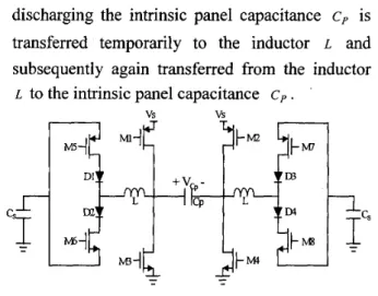
B. Parallel-Resonance Sustaining Driver [4]
The parallel resonance between the intrinsic panel capacitance
c,
and the external inductor Lin Fig.2 is the other energy recovery method. If the
voltage across the intrinsic panel capacitance
c,
initially is-v,
and the inductor current L is zero, then c,+c,
(2) 1 vc, ( t ) =-v, cos(-f)
.
JLCP
The equation (2) means that during one half of the resonance period the intrinsic panel capacitance
c,
can be charged again to the opposite polarity by a resonant current generated when the intrinsic panel capacitancec,
is discharged. The energy indischarging the intrinsic panel capacitance
c,
is transferred temporarily to the inductor L and subsequently again transferred from the inductorL to the intrinsic panel capacitance
c p .
Fig. I Series-resonance sustaining driver
M 3
Fig.2 Parallel-resonance sustaining driver
111. Influences of the Discharging Current on the Sustaining Drivers
Due to the generation of the ignited plasma discharging current when charging the intrinsic panel capacitance to exceed the firing voltage
vr
,something different affects the performance of the sustaining drivers. In order to evaluate the influence of the discharging current and avoid the degradation of the sustaining drivers, we should model the panel as a capacitance, parallel connected with a current source i d ( t ) . i d ( t ) can be
expressed as
(3)
T 0, t = t 2 - -
I
2where the voltage of the intrinsic panel
143
capacitance at t = tl is equal to the firing voltage
v,
and at the same time the discharging currentI~ is generated and maintained until t = t 2 . T
represents the resonance period. The simplified charging and discharging circuit of the series- resonance sustaining driver is illustrated in Fig.3. According to the initial conditions such as
v c p ( t = o ) = o , i L ( t = o ) = o , and vc,(t=o)=% the
2 '
following equation (4) can be derived and the voltage waveform across the intrinsic panel capacitance is drawn in Fig.4.
I I
The voltage across the lntnnslc Panel Capacitance
1%
time
Fig.4 Influence of the discharging current on the series- resonance sustaining driver
(Vs = 200V,Vf = 150V,Z, = 20A,t2 - t , = loons)
Fig.5 is the simplified charging and discharging circuit of the parallel-resonance sustaining driver. According to the initial conditions such as
vcP
( t = 0 ) = -V, and iL ( t = 0) =o ,
the following equation (5) can be derived and the voltage waveform across the intrinsic panel capacitance is drawn in Fig.6.I - vs cos(-I),
$
6
r=o-t,, t = t 1 - r 2 , ( 5 ) T r = I 2--
2 'Fig.3 The simplified charging and discharging circuit of the series-resonance sustaining driver
(C, = 20nF,Cs = 660pF,L = 5 p H )
L
Fig.5 The simplified charging and discharging circuit of the parallel-resonance sustaining driver (C, = 2OnF, L = 5,&)
144
The Voltage acro5s the lnlnnsl~ Panel Capacnance
I
0 5 1 1 5 2
x lo=
TtmHrec )
Fig.6 Influence of the discharging current on the parallel- resonance sustaining driver
(Vs = 200V, VI = 150V, Io = 20A,t2 - t, = 1 OOns)
Fig.7 is the experimental voltage waveform between the scanning and sustaining electrodes and the influence of the discharging current on the sustaining drivers is shown in the dashed-circle. From Fig.4, Fig.6 and Fig.7, the designed resonance condition is destroyed because the discharging current would dissipate some of the energy used to charge the intrinsic panel capacitance. Therefore, while the discharging current appears, the voltage across the intrinsic panel capacitance may decline sharply and the best power efficiency cannot be achieved by means of the previous switching time of the bi-directional switch. Furthermore, we find that using a smaller inductor is able to improve the decline of the voltage across the intrinsic panel capacitance somewhat but the inductor current becomes larger. Besides, from Fig.4 and Fig.6, the intrinsic panel capacitance could be charged to a higher voltage by the series-resonance charging circuit than by the parallel-resonance charging circuit. The reason is that the energy stored in the energy recovery capacitance can be served to generate the discharging current.
:“ ,---;:
, 100 \I I
Fig.7 The experimental voltage waveform between the scanning and sustaining electrodes
IV. Conclusion
According to the analysis in Section 11, we find that the parallel-resonance sustaining driver does not need the energy recovery capacitance cs in comparison with the series-resonance sustaining driver but the energy recovery function is also achieved. In addition, the discharging current would affect the performance of the two sustaining drivers. To reduce the influence on the sustaining drivers and still keep the best power efficiency, we should use a smaller inductor or adjust the switching time of the bi-directional switch.
V. References
J. P. Boeuf, L. C. Pitchford, “Calculated characteristics of an ac plasma display panel cell,” IEEE Trans. Plasma Science, vol. 24, pp. 95-96, 1996.
L. F. Weber, “Color plasma displays,” SID Int. Symp. Seminar Lecture Notes, voll , pp.611- 6/41, 1996.
L. F. Weber, K. W. Warren, “Power efficient sustain drivers and address drivers for plasma panel,” U.S. Patent Number 5,081,400.
M. Ohba, Y. Sano, “Energy recovery driver for a dot matrix ac plasma display panel with a parallel resonant circuit allowing power reduction,” U.S. Patent Number 5,670,974.
145