Influence of geometrical factors on angled broad-area semiconductor
lasers for high output power with good beam quality
Chih-Hung Tsai
a, Yi-Shin Su
a, and Ching-Fuh Lin
a, b aInstitute of Electro-Optical Engineering, National Taiwan University, Taipei, Taiwan, R.O.C.
bDepartment of Electrical Engineering and Institute of Electronics Engineering, National Taiwan
University, Taipei, Taiwan, R.O.C.
ABSTRACT
High-power semiconductor lasers with good beam quality are important for many applications. Angled broad-area waveguide structure could increase the output power and the beam quality is maintained at good quality. In this paper, we report the in-depth investigation on the geometrical factors that influence the performance of angled broad-area semiconductor lasers. The angled broad-area laser diodes are based on InGaAsP/InP materials. The waveguide is oriented at an angle from the normal of the cleaved facets. Our investigation shows that the waveguide width, the device length, and the tilted angle have to follow a certain relation in order to have the light propagate along a zigzag path inside the broad-area waveguide. When such a mode oscillates, the output light emits along the normal of the cleaved facet, showing no filamentation. Over 1 W of output power can be obtained with a good beam quality. Our investigation also discovers that devices with 100μm waveguide width perform better than devices with 50μm waveguide width.
Keywords: high-power semiconductor lasers, broad-area laser diode, beam quality, filamentation.
1. INTRODUCTION
High-power laser diodes offer a variety of advantages compared to gas or solid-state lasers such as small dimensions, low prices, and high efficiencies1. Many applications like material treatment, spectroscopy, and pumping of solid-state lasers and fiber amplifiers are possible using these high-power broad-area laser diodes2. Furthermore, high-power broad-area laser diodes can easily be fabricated in large quantities, offer high powers, and are available for a large spectral range. Broad Area Diode Lasers are high power diode lasers with output power values in the order of thousand milliwatts. In comparison to conventional Fabry Perot Diode Lasers, the emitter width is enlarged from typically ~3 -7μ m up to ~50-200μm3. Broad area diode lasers are spatially and longitudinally multimode mode4. Typical geometrical sizes of the laser chip are 1000μm x 500μm x 200μm (length x width x height). The laser chip is grown by metal organic vapor phase epitaxy (MOVPE) of compound semiconductor material. The optical gain is provided by double heterostructure which include several quantum wells for electronic confinement. The surfaces of the laser chip act as cavity mirrors due to the difference of the refractive index of the laser material and the surrounding air.
To make a diode laser emit optical power at thousands of milliwatts, the emitting facet must be large enough to prevent catastrophic optical damage (COD). Even with a high COD threshold (10MW/cm2)5, the emitting facet is required to be large to make COD threshold three times higher than the optical intensity for 1 watt operation. Thus, a high power diode laser is usually broad and flat. More than 30μm broad emitting facets are necessary for watt-range operation6. But the broad-area waveguide leads to the small difference of the threshold gain between the high-order modes and the fundamental mode7. In addition, the nonlinear interaction between carriers and light will produce filamentation of optical power distribution8-10. All these reasons make high-order transverse modes excited in broad-area Fabry-Perot laser diodes and the spatial coherence of emissions on every part of the facets is poor. It is important to resolve the filamentation problem and investigate a new type of semiconductor laser that can provide high power and the beam quality is maintained at good quality.
In this paper, we investigate a new type of broad area laser diodes that is capable of emitting good beam quality with watt-range output power and with good beam quality. For the new design of the waveguide, the laser diodes are fabricated with a broad-area waveguide that is oriented at an angle from the facet normal. Here we report the in-depth investigation on the geometrical factors that influence the performance of angled broad-area semiconductor lasers. The structures of the devices and the fabrication processes will be described in detail. Then, the measurement results of the laser diodes such as L-I curves, spectra, near fields and far fields will be described.
2. Device Structure
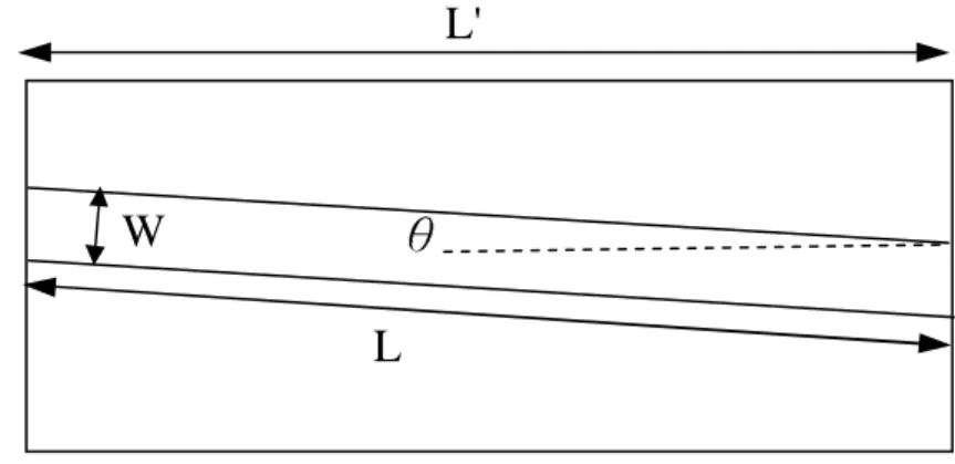
The fabrication of the device is a four-mask process. The laser diodes are fabricated on the wafer with multiple quantum wells (MQWs) designed for the wavelength at 1.3μm. Unlike conventional Fabry-Perot laser diodes, the waveguide direction is not perpendicular to the cleaved facet, but tilted at an angle. The devices have a double channel ridge waveguide created by reactive ion etching (RIE). The process gases are CH4 and H2. The channel button is 100nm~200nm above the undoped optical confinement layer. After the waveguide fabrication, silicon oxide grown by plasma enhanced chemical vapor deposition (PECVD) is used as the insulating dielectric. The contact metal is Ti/Pt/Au on the p-side and AuGe/Ni/Au on the n-side. No coatings are applied. After processing, the devices are cleaved apart. The cleaved device must be mounted on a copper heatsink for temperature control and ease of handling. The device is soldered on the heatsink by indium. The geometrical structure of the device is shown in Fig.1. W is the width, L is the length and θ is the tilted angle of the waveguide. L' is the length of the device. In the fabrication, θ=7°, W=50μm, L'=800μm, 1000μm, 1200μm length devices are cleaved, respectively. Another type of device is θ=6°,W=100μm, L'=1960μm.
Figure 1: Structure of the laser diode. W is the width, L is the length and θ is the tilt angle of the waveguide. L' is the length of the device.
3. Device Performance
Light-current (L-I) curve, spectrum, near field and far field are necessary to characterize a semiconductor laser. For a laser diode, operation threshold and efficiency are of great concern and can be obtained from L-I curve. The output beam quality is evaluated by measuring the near field and the far field. The spectral properties such as central wavelength and bandwidth can be obtained from spectrum. The devices with 50μm waveguide width are first introduced. The waveguide is tilted at 7°from the facet normal. The lengths of these devices are cleaved in 1200μm, 1000μm and 800μ m, respectively. Fig. 2 shows the L-I curve of the laser diodes. The threshold current of these devices is 1.2Amp. The devices have three regions of operation. The details of each region will be discussed in the following. Fig.2 shows the L-I curves of 1200μm, 1000μm, and 800μm, respectively.
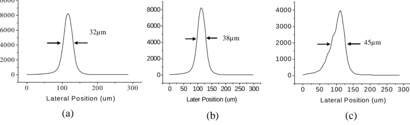
The laser diode with 50μm waveguide width and 1200μm device length is first described. As the current is below 0.6Amp, the output power is very low. Only 2mW output power is measured even when the pumping current is 0.5Amp. Fig. 3 shows the spectra of the 1200μm device. As the injection current is 0.5 Amp, the spectrum is broad with a full width at the half maximum (FWHM) of 42nm. The spectrum indicates that there is no oscillation in this region of operation. Fig. 4 and Fig. 5 show the near field and far field patterns of this device, respectively. When the current is 0.5 Amp, the FWHM of the near-field distribution is about 30μm and is mainly emitted from the waveguide region at the
L
W
L'
light path is approximately along the waveguide direction. Thus the output light is emitted at 24° from the facet normal according to the Snell's law.
Figure 2: L-I curves of the devices with 50μm waveguide width and (a) 1200µm (b) 1000µm and (c) 800µm device length As the pumping current is between 0.6Amp and 1.2Amp, the emission power significantly increases with the injection current. The output power is up to 40mW as the current is 1.2Amp. In this region of operation, the emission spectrum shrinks slightly. Fig. 3 (b) shows the spectra of the device at 1Amp. The FWHM of the spectrum is 26nm. Fig. 4 (b) and Fig. 5 (b) are the near field and far field patterns of this device at 1Amp, respectively. The near field slightly broadens and mainly distributes within the waveguide with a FWHM of 35μm at the facet.
Figure 3: Spectra of 1200µm device length at (a) 0.5A, (b) 1A, and (c) 6A
0 2 4 6 8 10 0 200 400 600 800 1000 P o w e r (m W ) Current (A) (b) 0 2 4 6 8 10 0 200 400 600 800 1000 P o w e r (m W ) Current (A) (c) 0 2 4 6 8 10 12 0 200 400 600 800 1000 Po w e r (m W ) Current (A) (a) Current: 0.5A 42nm Current: 1A 26nm Current: 6A 3nm 1200nm 1400nm
(a)
1100nm 1400nm(b)
1200nm 1400nm(c)
Figure4: Near fields of 1200µm device length at (a) 0.5Amp (b) 1Amp and (c) 6Amp
Figure5: Far fields of 1200µm device length at (a) 0.5Amp (b) 1Amp and (c) 6Amp
When the current is 1Amp, the horizontal far field has FWHM angle of 15°, which shrinks slightly in comparison with the measurement for current below 0.6Amp. The reduced spectral width, the increased output power, and the reduced far-field angle indicate that the light is amplified as it propagates along the waveguide because of the significant amplified spontaneous emission. As the pumping current is between 0.6Amp and 1.2Amp, the L-I curve also shows that the light power has significantly super-linear increases with the injection current. However, the device is not oscillating because the light path along the tilted waveguide provides no feedback in this region of operation. The high power and the broad spectral width make this device in this operation region a good candidate of high-power superluminescent diodes (SLDs). As the current is 1Amp, the light beam is emitted at 25°from the facet normal. It still satisfies the Snell's law. The reason for the reduced angle of peak emission is due to the carrier-induced reduction of refractive index at an increased injection current level.
When the current is beyond 1.2Amp, the laser oscillation begins. Output power of this device can increase up to 1 watt as the pumping current is 12Amp. The differential efficiency of this device is 0.12mW/mA per facet. Above the threshold current of 1.2Amp, the spectrum becomes very narrow. Fig. 3(c) shows the spectra of the device at 6Amp. The
0 30 60 90 120 150 180 0 40 80 120 160 Angle
(a)
0 100 200 300 0 2500 5000 7500 30µm Lateral Position (µm) Current: 0.5A 0 100 200 300 0 3000 6000 9000 35µm(b)
Current: 1A 60 70 80 90 100 110 120 0 200 400 600 800 1000 1200 1400 Angle4.5°
(c)
0 30 60 90 120 150 180 0 4000 8000 12000 Angle15°
(b)
0 100 200 300 0 1500 3000 4500 42µm Current: 6A22°
Lateral Position (µm)
(c)
Lateral Position (µm)(a)
However, the major power is still within the waveguide. The FWHM of the near field pattern is 42μm. The far field emits along the normal direction of the cleaved facet when the operation current is above 1.2 Amp. Fig. 5 (c) shows the far field pattern of the device for the pumping current of 6Amp. The horizontal FWHM of the far field pattern is 4.5°. This angle is only twice of the diffraction-limited value corresponding to the near field shown in Fig. 4(c). Fig. 5(c) also shows that a side lobe is at 24°from the facet normal and the FWHM angle of this lobe is 15°. In the L-I curve experiment, the brightness of both the normal lobe and side lobe are taken into account. The reason of the side lobe will be discussed later.
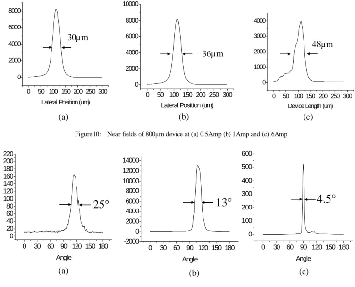
Fig. 6, Fig. 7 and Fig.8 show the spectra, near fields and far fields of the device with 50μm waveguide width and 1000μm length device at different injection current. Fig. 9, Fig. 10 and Fig.11 are the spectra, near fields and far fields of the 800μm length device at different injection current. Compare the results of 1000μm and 800μm length device with 1200μm length device, the threshold current, differential efficiency, spectra and near fields are similar. However, the far field is different from the 1200μm length device as the current is above threshold. The ratio of side lobe to normal lobe of 800μm length device and 1000μm are smaller than that of 1200μm. It indicates that the device length influences the far field patterns. As the device is operated above the threshold current, the measured spectrum of the 1000
μm device consists of many modes with the spectral spacing of 0.247nm. It indicates that the optical-path length is 1015 μm, which is longer than the device length. Thus the light path is zigzag instead of straight path oscillation. The mode
spacing of 1200μm device length is 0.198nm. It indicates that the optical-path length is 1219μm. The mode spacing of 800μm is 0.3nm, the optical-path length is 817μm. From these results, the light path is zigzag instead of straight path oscillation.
Figure 6: Spectra of the 1000µm device at (a) 0.5A, (b) 1A, and (c) 6A Current: 0.5A
45nm
1100nm 1500nm(a)
Current: 1A22nm
1250nm 1350nm(b)
3nm
Current: 6A 1200nm 1400nm(c)
Figure7: Near field of 1000µm device at (a) 0.5Amp (b) 1Amp and (c) 6Amp
Figure 8: Far fields of 1000µm device at (a) 0.5Amp (b) 1Amp and (c) 6Amp
(a)
0 100 200 300 0 2000 4000 6000 8000 10000L ateral P o sition (um )
32µm 0 50 100 150 200 250 300 0 2000 4000 6000 8000
Later Position (um)
38µm
(b)
0 50 100 150 200 250 300 0 1000 2000 3000 4000Lateral P osition (um)
45µm
(c)
0 30 60 90 120 150 180 0 3000 6000 9000 12000 15000 Angle20°
(a)
0 30 60 90 120 150 180 0 200 400 600 800 1000 Angle15°
(b)
0 30 60 90 120 150 180 0 500 1000 1500 2000 2500 3000 3500 Angle4.5°
(c)
Current: 0.5A42nm
(a)
1250nm 1350nm Current: 6A3nm
1250nm 1350nm(c)
Current: 1A28nm
1250nm 1350nm(b)
Figure10: Near fields of 800µm device at (a) 0.5Amp (b) 1Amp and (c) 6Amp
Figure 11: Far fields of 800µm device at (a) 0.5Amp (b) 1Amp and (c) 6Amp
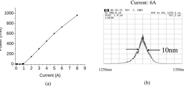
Another new type of high-power laser diodes with angled broad-area waveguide is also fabricated. The waveguide is tilted at 6°from the facet normal and the width of waveguide is 100μm. The lengths of these devices are cleaved in 1960μm. The L-I curves, spectra, near-field patterns and far-field patterns of the angled broad-area laser diode are measured. Fig. 12 (a) shows the L-I curve of this laser diode. The threshold current of this device is 1 Amp. The slope efficiency is 0.15W/A. The output power can achieve 1W per facet when the current is 8Amp. The spectrum above the threshold is shown in Fig. 12 (b). The lasing wavelength is centered at 1.3μm with a FWHM spectral width of 10nm. The measured spectrum consists of many modes with the spectral spacing of 0.122nm. It indicates that the optical-path length is 1978μm. Near-field patterns and far-field patterns are also measured. Fig. 13 (a) shows the near-field pattern and Fig. 13 (b) shows the far-field pattern of the device. From the near field, it shows that the output light is mainly emitted from the waveguide region. The width of the near-field distribution is around 40μm. No filamentation is observed. The corresponding diffraction-limited angle of the far field is 2.27°. As the pumping current is above the threshold current, the light beam emits from the facet normal. The far field pattern shows that light does not go along the tilted waveguide. Instead, it goes straight out of the facet. The FWHM of the far field is 4.2°, which corresponds to 1.85 times of the diffraction-limited value of the near-field pattern.
0 30 60 90 120 150 180 0 20 40 60 80 100 120 140 160 180 200 220 Angle
25°
(a)
0 30 60 90 120 150 180 -2000 0 2000 4000 6000 8000 10000 12000 14000 Angle13°
(b)
0 30 60 90 120 150 180 0 100 200 300 400 500 600 Angle4.5°
(c)
0 50 100 150 200 250 300 0 2000 4000 6000 8000Lateral Position (um)
36µm
0 50 100 150 200 250 300 0 2000 4000 6000 8000 10000Lateral Position (um)
0 50 100 150 200 250 300 0 1000 2000 3000 4000
Device Length (um)
(a)
(b)
(c)
36µ m
48µ m
30µ m
Figure 12: (a) L-I curve and (b) Spectrum of 100μm waveguide width and 1960μm device length laser diode
Figure 13: (a) Near field and (b) far field of 100μm waveguide width and 1960μm device length laser diode
4. Discussion
To estimate the optical-path in the waveguide, the formula D = λ2 / 2nΔλ is used, where λ is oscillation wavelength, D is the optical-path, n is the refraction index of the waveguide and Δλ is the mode spacing. The factor n is first determined by the mode spacing measurement of a 1.31μm wavelength and 700μm long Fabry-Parot laser diode. The mode spacing of 700μm device length is 0.35 nm. Then the refraction index n=3.5 can be obtained by using D = λ2 / 2nΔλ formula. The mode spacing of 1200μm device length is 0.198nm. It indicates that the optical-path
Current: 6A
10nm
1250nm 1350nm 0 1 2 3 4 5 6 7 8 9 0 200 400 600 800 1000 Po w e r ( m W) Current (A)(a)
(b)
0 100 200 300 400 500 600 0 1000 2000 3000 4000Lateral position (um)
40µm
0 30 60 90 120 150 180 0 300 600 900 1200 1500 1800 Angle4.2 º
Current: 6A
Current: 6A
(b)
(a)
For such a mode to oscillate, the device length should be properly chosen to satisfy the zigzag path11. The optical-path length would be D=2mW/sin(θ), the waveguide length would be L=2mWcos(θ) / sin(θ), and the device length would be L'=2mWcos(θ) / tan(θ), where m is any positive integer. m=1 means that light in the waveguide is reflected twice at the waveguide boundary. Too long or too short waveguide for the devices will cause some portion of the output beam to emit toward other directions. For W=50μm and θ=7°, L' should be 808μm. Therefore, Fig. 5 (c) shows that the far field of a 1200μm length device has the side lobe emitted at about 24°from the facet normal because some portion of the light still propagates along the waveguide instead of the zigzag path. The side lobe almost vanishes for the 800μm device. This kind of light path can average out the fluctuation induced by the interaction between carriers and light, so filamentation is significantly reduced. Compare 50μm waveguide widthμm with 100μm waveguide width device, the slope efficiency of 100μm waveguide width is 0.15W/A and the slope efficiency of 50μm waveguide width is 0.12W/A. It shows that devices with 100μm waveguide width perform better than devices with 50μm waveguide width. For the magnitude of the tilted angle of the waveguide is considered, the tilted angleθshould be properly chosen to satisfy the formula L'=2mWcos(θ) / tan(θ).
5. Conclusion
In conclusion, a new type of angled broad-area waveguide laser diodes is fabricated on a substrate with MQWs designed for 1300nm. These device lengths are 1200μm, 1000μm, and 800μm. The waveguide is 50μm wide and tilted at 7°from the facet normal. The devices have three regions of operation. For the injected current between 0.6Amp and 1.2Amp, it behaves like a SLD with a spectral width of about 40 nm and the output power of 40 mW. Without facet coating, as the current is above 1.2Amp, this device oscillates and could emit 1 W output power per facet at 12Amp. The far field pattern has direction changes between below and above the threshold current. When the device is oscillating, the far field emits along the facet normal. The horizontal far-field angle is only twice of the diffraction-limited value. Compared with conventional broad area waveguide lasers, the near field patterns of angled broad area lasers are smoother and almost free of filamentation. No DFB or photonic-crystal structures are required, the fabrication is much simpler and suitable for mass production. A 100μm waveguide width angled broad-area semiconductor laser has also been fabricated. The device perform better than devices with 50μm waveguide width. It could emit 1 W output power per facet at 8 Amp. Under proper design of the geometrical factors, the beam quality is good and the near field shows no filamantation. The horizontal far-field angle is only twice of the diffraction-limited value.
6. References
1. P. Bousselet, C. Simonneau, C. Moreau, L. Provost, P. Lambelet, X. Rejeaunier,F. Leplingard, L. Gasca, and D. Bayart, “+33 dBm output power from a full C-bandcladding diode-pumped EDFA,” in ECOC 2002, Copenhagen, 2002.
2. C. Codemard, K. Yla-Jarkko, J. Singleton, P. W. Turner, I. Godfrey, S.-U. Alam,J. Nilsson, J. Sahu, and A. B. Grudinin, “Low noise, intelligent cladding pumpedl-band EDFA,”in ECOC 2002, Copenhagen, 2002.
3. P. Loosen, H.-G. Treusch, C. R. Haas, U. Gardenier, M. Weck, V. Sinnho, St. Kasperowsky, and R. vor dem Esche, "High-power diode lasers and their direct industrial applications," SPIE Proc.2382, pp.75-78, 1995.
4. S. D. de Mars, K. M. Dzurko, R. J. Lang, D. F. Welch, D. R. Scifres, and A. Hardy, "Angled grating distributed-feedback laser with 1W single-mode, diffraction-limited output at 980nm," Techn. Digest CLEO 96, pp.77-78, 1996.
5. M. Mikulla, "Improved beam quality for high-power tapered diode lasers with LMG eptitaxial layer structures," SPIE Proc.3284, pp.72-79, 1998.
6. M. Fukuda, "Reliability and degradation of semiconductor lasers and LEDs", Boston, MA: Artech, 1991.
10. M. A. Emanuel, N. W. Carlson, "High-efficiency AlGaAs-based laser at 808nm with large transverse spot size," IEEE Photon. Technol. Lett., vol. 8, pp.1291-1293, 1996.
7. Jie-Wei Lai and Ching-Fuh Lin, "Carrier diffusion effect in flared semiconductor-laser amplifier," IEEE J. Quantum Electron. 34, pp.1247-1256, 1998.
8. J. S. Osinski, K. M. Dzurko, J. S. Major, R. A. Parke, D. F. Welch, " Electronically tunable, 1 W CW, diffraction-limited monolithic flared amplifier-master oscillator power amplifier (MFA-MOPA)," Semiconductor Laser Conference, 1994., 14th IEEE International, p.161-162, 1994.
9. D. Mehuys, D. Welch, and L. Goldserg, "2W CW Diffraction-limited Tapered Amplifier With Diode Injection," Electron. Lett. Vol. 28, No. 8, 1992.
10. W. D. Herzog, B. B. Goldberg, and M. S. Unlu, "Beam steering in narrow-stripe high-power 980-nm laser diodes," IEEE Photonics Technology Letters, Vol.12, No.12, 2000.
11. Chih-Hung Tsai, Yi-Shin Su, Chia-Wei Tsai, D.P. Tsai and Ching-Fuh Lin, "High-power angled broad-area 1.3μm laser diodes with good beam quality," IEEE Photon. Technol. Lett., vol.16, pp.2412-2414, 2004.