Leakage Performance and Breakdown Mechanism of
Silicon-Rich Oxide and Fluorinated Oxide Prepared by
Electron Cyclotron Resonance Chemical Vapor Deposition
Kow Ming Chang, ShihWel Wang,Ta I-hun Yeb, Cliii Horng Li, and Jiunn Jye Luo
Departmentof Electronic Engineering and Institute of Electronics, National Chiao Tang University, National Nano Device Laboratory, Hsinchu, Taiwan
ABSTRACT
The characteristics of silicon-rich oxide and fluorinated oxide (FSiO4) films deposited in an electron cyclotron res-onance chemical vapor deposition system with SiR4 and 02 as the oxide sources and CF4 as the fluorinating precursor are investigated in this work. According to experimental results, the dangling bonds in Si-rich oxide behave as positively by charged electron traps and degrade the dielectric strength by lowering the barrier height for Fowler-Nordheim tunnel-ing. On the other hand, a small amount of incorporated F atoms will passivate and neutralize these excess Si dangling bonds, thereby elevating the dielectric strength. However, too much incorporated F will degrade the pretunneling leak-age performance owing to the porosity and fatigues structure in FSiO4 film. The high leakleak-age and even breakdown at low field strongly limits the incorporated F concentration in FSi04 film and the lowering of dielectric constant.
Infroduction
Advancesin ultralarge-scale integrated circuits have led to the necessity for an intermetal dielectric (TMD) with the dielectric constant (k) as low as possible to overcome the limitation of signal delay. As a candidate for low-k IMD material, chemical vapor deposition of inorganic fluori-nated silicon oxide (FSi04) has received extensive interest due to its easily integratable properties and various read-ily available precursorst'2 In addition to low dielectric constant, maintaining the other properties desirable for
IMD applications (such as low leakage current, low
mechanical stress, high thermal stability, and low mois-ture absorption) is also important. However, only a few studies have been published on these issues,"13 especially for those dedicated to the leakage performance and dielec-tric strength of FXSiOY. On the other hand, Si-rich oxide
(Si03, p
2) prepared by electron cyclotron resonance chemical vapor deposition (ECR-CVD), capable of pre-venting moisture permeation and avoiding hot carrier effects, is very important to back-end applications.'2"7 Similarly, there has been very little work on the leakage performance and dielectric strength of ECR-Si04.In this work, ECR-CVD Si-rich SiO,,, and FXSiOY films for IMD applications were fabricated, with SiR,, and 02 as the oxide sources and CF4 as the fluorinating precursor. According to experimental results, the change in stoi-chiometry, controlled by the flow ratio of SiH4/02, heavily affects the dielectric constant and electrical performance of Si-rich SiO3. The excess Si dangling bonds, acting as positively charged electron traps, are shown to degrade the dielectric strength of the oxide. On the other hand, not only reducing the dielectric constant, the small amount of incorporated F atoms will passivate and neutralize these excess Si dangling bonds and be of benefit to the dielectric strength of the deposited film. However, too much incor-porated F leads to a porous and fatigued oxide network, The pretunneling leakage performance of FXSiOY is found to degrade with the increase of F concentration and even break down at a low field. Such an event strongly affects the reliability and applicability of FSiO5. The mecha-nisms contributing to these results are discussed in this paper.
Experimental
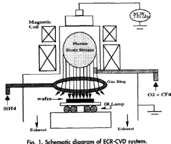
Figure1 shows the schematic diagram of the FCR sys-tem used in this work. High-density plasma of 02/CF4 was ignited by microwave (MW) with a frequency of 2.45 GHz and magnetic field at 875 G. The 02/CF4 plasmas down-stream and react with SiH4 injected from the gas ring. The SiO and FSiO4 films were deposited on 4 in., (100)-ori-ented, p-type silicon wafers. The wafers were treated with
RCA cleaning and dipped in HF solution (1/100) before loading. The 02 flow rates were fixed at 85 sccm while the SiH,, flow rates were varied from 2 to 10 sccm, and the CF4 flow rates were varied from 0 to 20 sccm. The deposition pressure was kept at 3 mTorr. The deposition temperature (T) was varied from 25 to 300°C and MW power was set at 250 or 300 W.
The composition and chemical bonding structure of deposited films were investigated by x-ray photoelectron spectroscopy (XPS) and Fourier transform infrared spec-troscopy (FTIR), respectively. The dielectric constants (k) were measured from C-V characteristics using a Keithley C-V system with a simple metal-insulator-semiconductor (MIS) structure at 1 MHz. The refractive index and thick-ness of the deposited films werc determined by ellipsome-try at a frequency of 632.8 nm (He-Ne laser). The I-V char-acteristics and variation of voltage drop on the deposited film, under constant current stress, were investigated by using an HP4145B system with MIS structure.
Resultsand Discussion
Figure2 depicts the typical XPS spectra of ECR-Si04
(CF4 = 0sccm) and FXSiO4 films. Four main elements: Si
(2s, 2p), C (is), 0 (Is), and F (is), are observed in the
deposit-ed films. The incorporatdeposit-ed F concentration (is, 687 eV) increases with the increased CF4 flow rate. The high flow ratio of 02 to CF4 effectively limits the concentration of incorporated C to less than 2 atomic percent (a/o) due to
1754 J. Electrochem. Soc., Vol. 144, No. 5, May 1997 The Electrochemical Society, Inc. Fig. L Schematic diagram of ECR-CVD system.
J. Electrochem. Soc., Vol. 144, No. 5, May 1997 © The Electrochemical Society, Inc. o. Cn 0 CU 700 600 500 400 300 200 100
Binding Energy (eV)
Fig. 2. Typical XPS spectra of the FSiOy film with different CF4
flow rates.
the oxidation effect. Quantitative measurement from XPS spectra also demonstrates that ECR-SiOy is nonstoichio-metric and Si-rich in composition. From Fig. 3a, a higher flow ratio of SiH4 over 02 results in a richer Si in oxide
composition. From FTIR spectra, such stoichiometric change of oxide with SiH4/O, flow ratio is reflected in the
variation of Si-O-Si stretching vibration frequency, as shown in Table I. The stretching vibration frequency of ther-mal oxide (1000°C, 0, dry oxidation) is about 1087.7 cm-'. On the other hand, for ECR-SiO, films deposited at 300°C, the vibration frequency shifts from 1074.4 cm-' for SiH4/O, = 2/85 sccm, to 1057.6 cm ' for SiH4/O2 = 10/85
sccm. According to the work of Kobeda et al.,"8 the stretch-ing vibration frequency (v) of Si-O-Si in glass network depends on its common angle [0, where v cc sin (0/2)]. Additionally, the Si-rich oxide tends to have a smaller 0 according to the structure-induced charge-transfer model (SICT).'9Therefore, the decrease of Si-O stretching vibra-tion frequency accounts for the richer Si in oxide compo-sition. The richer Si in ECR-SiO, oxide results in a higher dielectric constant (k) than that of stoichiometric thermal oxide, as shown in Table I. This is due to the excess Si (dangling bonds) which results in the strain and disturbs the balance position of other atoms in ideal oxide and induces an excess dipole moment.
Not only the stoichiometric ratio of Si over O, the SiH4/O2flow ratio also affects the incorporated F
concen-tration in FSiO when CF4 is added. The stoichiometry y
value of FSiOy film almost keeps constant, while the x value monotonically increases with an increasing CF4 flow
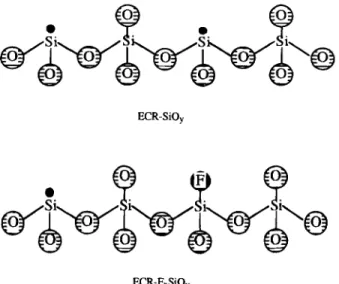
rate (0 to 20 sccm), as shown in Fig. 3a and b, respective-ly. This result demonstrates that with both behaving as the electron acceptors, there is no competition between active F and O species if there is enough Si source for a reaction. The incorporated F atoms passivate and reduce the Si dangling bond concentration with the formation of Si-F bonds, as shown in Fig. 4. Moreover, the ECR-FSiOy with richer Si in composition (i.e., higher SiH4/O, ratio) will
involve more incorporated F. In Fig. 3a and b, the incorpo-rated F concentration rises from 3.9 a/o for SiH,/O, =
1.85 1.80 1.75 I n I.65 1.65 1.60 1 ,c .JJ 1.50 1.45 0.20 0.15 0.10 0.05 0.00 o SiH4 = 4 sccm 0 SiH4 = 8 sccm a SiH4 = 10 sccm 0O O O T0 o o Oo 0 ... . ... M/,W 250W, 25°C, 02 = 85 sccm: 0 5 10 15 20 25 CF4 Flow Rate (sccm) (a) MW 250W, 250C, 02 = 85 sccm 0 , 0 0 SiH4 4sccm _°o [ D] 0 0 SiH4 = 8 sccm A SiH4 = 10 sccm . I . I ...-0 5 10 15 20 25 CF4 Flow Rate ( sccm )
Fig. 3. Variations of (a) y value and (b) x value in stoichiometry of FSiOy films, with different SiH4, CF4flow rates.
4/85, 4.6 a/o for SiH4/O, = 8/85, toward 5.9 a/o for
SiH4/O, = 10/85 sccm, with the same CF4 (20 sccm) added.
The dielectric constant of F.SiOy film also decreases from 3.13 for SiH4/O2/CF4 = 8/85/20 sccm to 2.98 for
SiH4/O2/CF4 = 10/85/20 sccm, correspondingly.
According to the work of Takahashi et al.,'4 the dangling bonds belonging to Si atoms in ECR oxide are amorphous centers (Si3 = Si-) and E' centers (, Si-) or oxygen
vacancies. The water-blocking ability comes from these defect centers and hydrogen-passivated Si bonds (Si-H).'4-"7 The hot carrier degradation was shown to be reduced with increasing the SiH4/O2flow ratio during deposition of the
ECR-SiOy water blocking layer." Unfortunately, according to our experimental results, the dielectric strength of ECR-SiOy heavily degrades with an increasing SiH4/O2
flow ratio. Figure 5 shows the time-zero dielectric break-down characteristics of thermal oxide (1000°C, 0, dry oxi-dation) and ECR-SiOy films (300°C, with various SiH4/O2
flow ratios) taken at room temperature. The thickness of
Table I. Changes in FTIR Si-O stretching vibration frequency, dielectric constant (1 MHz), and barrier height for Fowler-Nordhein tunneling'2 at an Al-insulator interface for thermal oxide (dry oxidation) and ECR-CVD oxides (3000C, MW 300 W, 85 sccm 02) deposited
with various SiH4flow rates.
Insulator type FTIR Si-O stretching peak Dielectric F-N barrier height
(-100 nm) (cm-') constant (eV)
Thermal oxide (0,, 1000'C) ECR oxide, 2 seem SiH, ECR oxide, 4 seem SiH4 ECR oxide, 8 seem SiH, ECR oxide, 10 seem SiH4
1087.7 1074.4 1066.6 1059.3 1057.6 3.98 4.22 4.39 4.51 4.57 3.304 2.316 2.259 2.248 0.533 1755 i
1756 .1 Electrochem. Soc., Vol. 144, No. 5, May 1997 The Electrochemical Society, Inc.
0
0
ECR-SiO ECR-F5SiO -5 -4 -3 -2 -1 0 1.2 t.0 0.8 0 0.6 LI 0.4 0.2 0.0 V (volts)Fig.6. High-frequency C-V characteristics of thermal oxide,
[CR-Si07 and F,,5i08 (MW 300 WI 3 mlorr and 300°C), with thickness around 100 nm.
tronsresult in impact ionization near the anode (>9 eV)26 due to the large voltage drop on the oxide even under a low
electric field. Therefore, dielectric strength rapidly
degrades with an increasing SiH4/02 flow ratio.
Concurrently, a large amount of defect centers (E' center and Si—H bonds) in Si-rich oxide is also responsible for dielectric breakdown.23 Researchers on E' centers have suggested that they act as hole traps,27 some electron traps,28 and still others that they are both electron traps and hole traps.29-33 In the present work, the trapping
cen-ters in ECR-Si05 are shown to be electron traps and
increase in amount with the SiH4/02 flow ratio. Figure 7 reveals the changes of voltage drop on the oxide (Al V0-VFBI) under constant current stress in the range of F-N tunnel-ing. The increase of voltage drop, required to maintain a constant current, reflects the existence of electron trap-ping centers in oxide.34 It is found that the voltage drop on thermal oxide almost keeps constant without change, while the voltage drop on ECR-Si09 increases during stress. On the other hand, the change of voltage drop on ECR-Si00 also increases with increasing the SiH4/02 flow ratio under the same charge fluence. As a result, the rich-er the Si in oxide composition, more trapping centrich-ers are present. The Si dangling bonds may be passivated with —H bonds in more humid air. However, the Si—H bonds are eas-ily broken by energetic electrons (>2 eV)20 and become E'
30 25 20 0 '— 15
a
>- 10 ci 0 -5 -10 30 40 50 60 Injected Charge ( >< 62.5 nC/cm2)Fig. 7. The changes of voltage drop (Al Va — I) on various
oxide films during the constant current stress The stress current was
0.1 nA with density —623 nA/cm2, in the range of F-N tunneling. Fig. 4. Hypothesized local structures in Si-rich ECR-5i07 and
F,SiO film networks. Part of Si dangling bonds (•) are passivated with bonds with the addition of CF4.
alldielectrics is around 100 nm. Polarity of the field caus-es carrier accumulation at the Si surface corrcaus-esponding to electron injection from the metal gate. The breakdown field degrades rapidly with the increasing SiH4/02 flow ratio, in comparison to that of near-stoichiometric thermal oxide. From the current density (3) vs. electric field (F) curves, the linearity for the in (.1/F2) vs. 1/F relationship demonstrates that the barrier for Fowler-Nordhein tun-neling20 generally decreases with increasing the SiH4/O2 flow ratio, as shown in Table I. The measured slope, corre-sponding to barrier height at the aluminum/oxide interface, drops from 3.304 eV for thermal oxide toward 0.533 eV for ECR-SiO5 with SiH4/O2 = 10/85 sccm. According to
Maserjian and Zamani,2' Balland,22 and Hasegawa et at. theoxygen vacancies induce positive fixed charges in the oxide. Figure 6 compares the high-frequency C-V curves for well-controlled thermal oxide and Si-rich ECR-Si09. The negative shifting of flatband voltage (VEB) accounts for the existence of positive charges in ECR-SiO94. As a result,
the barrier lowering is assumed to be due to the image
force effect of positive oxide charges acting on the
metal/oxide interface.24 In addition, the local potential well of positive charged centers also contributes to the tunneling current.25 For a thick oxide, the injected
elec-10.10
-iooo°coon&
—fl-—— S1H4IO2 =4185scemö
io.'
—a-—— 5014/02=8/85scm
-—a---— S1H4/02 =10/85sccm -—14 • I I I I • I • I I • I I 10 0 -2 -4 -6 -8 -10 -12 Electric Field ( MV/cm)Fig. 5. Time-zero dielectric breakdown characteristics of the
thermal oxide (dry oxidation, 1000°C) and the ECR-5i01 films
(MW 300 W, 3 mTorr, and 300°C) deposited with different SiH4/02
flow ratios. A 1000°C Dry Oxide 51114/02=2/85seem. 300°C
•
51114/02 = 8/85seem, 300°C S1H4/02/CF4=8/85/4 seem, 30(1°C -0--— Sil-14/02/CF4 =8/85/10seem, 0 10 20J. Electrochem. Soc., Vol. 144, No. 5, May 1997 The Electrochemical Society, Inc. 1757 ,.. E r1 = L)
centers again. This result supports the conclusion in
Hasegawa et al's work.23 From literature reviews,3539 elec-tron traps contribute to dielectric breakdown because the trapping of injected electrons will modulate the conduc-tion band of the oxide and increase the positive feedback current.
On the other hand, it was found that the dielectric was strengthened with suitable incorporation of F. Figure 8 compares the time-zero dielectric breakdown characteris-tics of the ECR-SiO and FSiO films deposited at 300°C. The destructive breakdown fields of ECR-SiO films (with SiH4/02 =8/85and 10/85 seem) were enhanced with a lit-tle CF4 added (4 seem). From previous discussion and the comparison between C-V curves of ECR SiO,, and FSiO in Fig. 6, the incorporated F atoms passivate and neutral-ize the positive charged Si dangling bonds with the for-mation of Si—F bonds. The decrease of positive charges in
the oxide accounts for the positive shifting of the C-V curve with the addition of CF4. Therefore, the image force
effect on barrier lowering, due to the positive oxide
charge, is suppressed and responsible for the enhancement of breakdown field. From Fig. 8, the barrier height for F-N tunneling at the aluminum/oxide interface increases from 2.248 eV of ECR-SiO (SiH4/02 =8/85seem) to 2.288 eV of
FSiO (SiH4/02/CF4 = 8/85/4 seem), correspondingly. The Si—F bond has been shown to have higher strength (—5.73 eV) than that of the Si—H bond (—5.45 eV) to resist energetic electrons.4° Such a decrease in electron trap concentration with the addition of CF4 will be ref lect-ed in the change of voltage drop on the oxide during con-stant current stress. As shown in Fig. 7, the change of volt-age drop during stress on FSiO, with SiH4/02/CF4 = 8/85/4 seem, is suppressed compared to that on ECR-.SiO without adding CF4.
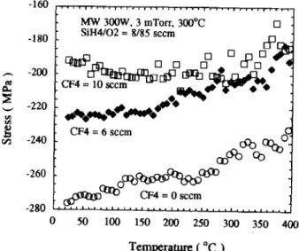
However, the pretunneling leakage performances of FSiO were found to degrade with further increasing the CF4 flow rate. As shown in Fig. 8, the preturmeling leak-age current of FSiO, with a higher amount of incorporat-ed F (SiH4/O2/CF4 = 10/85/12 seem) ramps-up rapidly with field and even wears out a low field. Such a degrada-tion of pretunneling leakage performance heavily impacts the applicability of FSiO within the normal operation range of IMD. According to experimental results, the high leakage current strongly correlates to the porous, fatigued structural network of FSiO. From prior reports,'213 the incorporation of F results in a porous oxide network due to its high electronegativity in nature and nonbridging ter-mination with Si atoms. The porosity of the oxide can be determined from the changes in refractive index,'2 mois-ture permeation,'2 deposition rate,'3 and mechanical stress during the thermal cycle, with the addition of CF4. Fig-ure 9 depicts the variation of film stress during thermal
cycling (25 to 400°C) with different F concentrations. The measured stress (crt,,,) for the deposited film is the combi-nation of intrinsic stress (or,,,,) and thermal stress (th).4'The intrinsic stress is created when the film network is formed while the thermal stress is induced by the difference between the thermal expansion coefficient of the Si sub-strate (as)andthat of the deposited film (a,) when the film is cooled from the deposition temperature (Td,P)toroom temperature (TRT)
0total = 0int + 0th [1]
0th = [j__](as — af)(TRT —
TdepO) [2]
In Eq. 2, E and v stand for Young's modules and Poisson's ratio of the deposited film, respectively. In Fig. 9, the high-er thhigh-ermal expansion coefficient of the Si substrate than that of the oxide in the elastic range contributes to the compressed stress of deposited films. The 300°C deposited FrSIOy film does not absorb moisture'2 and shows no hys-teresis variation in stress during thermal cycles. This means no plastic deformation and structure change in the deposited film during the thermal cycle, and the stress at 300°C will be the intrinsic component. Therefore, the intrinsic (compressed) stresses are shown to relax with the addition of F On the other hand, the stress variation with temperature in the elastic range is governed by the follow-ing equation
______= .!?ii- =[———1(a — a ) [3] dT
dT L1v]
From Fig. 9, the dath/dT of the oxide decreases with the incorporation of F. This is due to the decrease of E or the increase of a1. In FSiO films, the F atom forms a non-bridge terminal bond on one Si atom without linking to
the other Si atoms. Additionally, the repulsive force
between Si-F and Si-F bonds, or Si-F and Si-O bonds, further fatigues the oxide structure; thus, the resulting less rigid glass network and lower Young's modulus are reasonable.
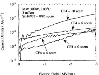
Figure 10 reveals the general effect of incorporated F concentration on the pretunneling leakage performance of FSiO films about 250 nm thick. The leakage current den-sity is about 1 nA/cm2 at 1 MV/cm for ECR-SiO, and there
is about an order of magnitude increase (—20 nA/cm2) when 10 seem of CF4 is added. On the other hand, a lower
-160 -180 io-3
l0
10"
-200 -220 -240 -260 -280 MW 300W, 3 mlorr, 300°C0
S1H4/02 = 8/85 sccmo0p
nfL-
0
D 0
0
CF4 =10
CF4 = 6 sccm GD CF4 0 seem 0 -2 -4 -6 -8 -10 Electric Field ( MV/cm)Fig.8. Time-zero dielectric breakdown characteristics of ECR-SiO
and F,SiO films deposited with different Sil44/02/CF4 flow ratios (MW 300 W,3 mlorr and 300°C).
0
50 100 150 200 250 300 350 400
Temperature (°C)Fig.9. Variation of mechanical stressduringthermal cycles, from
25 to 400°C, for ECR-SiO and F,SiO films deposited with different
1758 .J. Electrochem. Soc., Vol. 144, No. 5, May 1997 The Electrochemical Society, Inc. E a '2 a Eleciric Field (MV/cm)
Fig. 10. Variation of FSiO2 film pretunneling leakage
perfor-mance with different CF4 flow rates.
deposition temperature has been shown to result in a less dense stack and a higher, but unstable, incorporated F concentration in FSiO2 film.'2 Figure 11 depicts the gen-eral variation of pretunneling leakage current with elec-tric field for the FSiO2 films deposited at various temper-atures. The leakage performance generally degrades with decreasing deposition temperature. Besides, thermal sta-bility of F also demonstrates the correlation between the F concentration and leakage performance. From prior
work,'2 FXSiOY films deposited at 300°C were able to withstand annealing temperature above 700°C (N2 ambi-ent, 30 mm) while the films deposited at 25°C could only withstand temperature about 500°C. Here we find that the leakage performance of FSiO4 films shows a similar ten-dency. Figure 12 depicts the pretunneling leakage of 3 00°C deposited film and those with subsequent annealing at 500, 600, 700, and 800°C (N2 ambient, 30 mm). Only slight changes were found at annealing temperatures above 700°C. On the other hand, the leakage performance of FXSiOY films deposited at 25°C shows profound changes after each temperature annealing, as shown in Fig. 13.
From this evidence, it can be seen that F incorporation indeed elevates the low-field leakage current in FXSO, films. Although the Si dangling bonds can be passivated by F atoms, the porous structure and even micropores existing in the FSiO2 network additionally induces hole
trap formation. Such an event can be realized by the
decrease of voltage drop on FSiO2, with SiH4/02/CF4 =
Electric Field (MV/cm)
Fig.12. Variation of pretunneling leakage performance for FSiO
films, deposited at 300°C, before and after annealing at 500,
700, and 800°C (30 mm in N2 ambient).
8/85/12 sccm, during the constant current stress, as shown in Fig. 7. According to Dumin and Muddux,42 Rofan and flu,43 and Olivo et al.,44 stress-induced traps and defects or weak spots in thin oxide are responsible for the excess low-level pretunneling current. In the present work, the fatigued structure and traps, contributing to a high pre-tunneling leakage current and catastrophic breakdown at
low field through localized weak spots, are induced with the incorporation of F Therefore, the power consumption and reliability problems which arise will limit the incor-porated F concentration and hence the lowering of the dielectric constant of FSiO2 for IMD applications.
Conclusions
In summary, the stoichiometric change in Si-rich ECR-SiO relies on the flow ratio of SiH4 over 02. The Si dan-gling bonds (E' centers or oxygen vacancies) behave as the electron traps with positive charged. The image force induced by these positive oxide charges, effectively lower-ing the barrier height on aluminum/oxide interface for
Fowler-Nordhein tunneling, heavily degrades the break-down strength of ECR-Si02 with an increasing SiH4/03 flow ratio. On the other hand, in a suitable amount, the incorporated F atoms are shown to passivate and neutral-ize these charged traps, which benefits the breakdown field of FSOr However, nonbridge Si-F termination and repulsive force between F and 0 atoms result in a porous
Electric Field (MV/cm)
Fig. 11. Variation of F,5i07 film pretunneling leakage
perfor-mance with different deposition temperatures.
Fig. 13. Variation of pretunneling leakage performance for FXSiOJ,
films, deposited at 25°C, before and after annealing at 400, 500, 600, 700, and 800°C (30 mm in N2 ambient). 1W6 io8 U '4: a '2
0
I
io'o 0 -l -2 no-annealing, 500°C,600°C MW 300W, 3 mToxr 300°C SiH4/02/CF4=8/85/10sccm l010 0.0 -1.0 -2.0 -3.0 -4.0 -3 10.6 E -12 2-a 430
I
l0
E 2-aC0
I
i o5 106i
o-7 10.8 io9 10.10 io-'o MW 300W, 3niTorr SiH4/02/CF4= 8/85/10 sccm 0-l
-2 -3 -4 MW 300W, 3mTorr Room Temperature S1H4/02/CF4 =8/85/10sccm 0 -1 -2 -3 -4 -5 Electric Field (MV/cm)J. Electrochem. Soc., Vol. 144, No. 5, May 1997 The Electrochemical Society, Inc. 1759
oxide network and hole traps. The excess low-level pre-tunneling leakage current was shown to increase with the incorporated F concentration and even wear out and break down at low field through localized weak spots. Therefore, too much F incorporation in FrSOY raises power consumption and reliability problems. The
incorpo-rated F concentration and hence the lowering of the
dielectric constant of FSiO will be limited. Acknowledgment
Thiswork is supported under Taiwan R.O.C. National Science Council Contract No. NSC 85-2215-E009-061.
Manuscript submitted July 1, 1996; revised manuscript received March 5, 1997.
National Chiao TungUniversityassisted in meeting the publication costs of this article.
REFERENCES 1. R. K. Laxman, Semicond. mt., 71 (1995).
2. T. Fukada and T. Akahori, in Proceedings of the First International Dielectrics for VLSI/ULSI Multilevel Interconnection Conference, p. 43, IEEE, Santa
Clara, CA (1995).
3. L. A. Quain, H. W. Fry, G. Nobinger, J. T. Pye, M. C. Schmidt, and J. Cassillas, ibid., p. 50 (1995). 4. 5. Takeishi, R. Shinohara, H. Kudoh, A. Tsukune, Y.
Satoh, H. Miyazawa, H. Hrada, and M. Yamada,
ibid., p. 257 (1995).
5. T. Homma, R. Yamaguchi, and Y. Murao, This Journal, 140, 680 (1993).
6. T. Usami, K. Shimokawa, and M. Yoshimara, Jpn. J. Appl. Phys., 33, 408 (1994).
7. T. Matsuda, M. J. Shapiro, and S. V. Nguyen, in Proceedings of the First International Dielectrics for VLSI/ULSI Multilevel Interconnection Conference, p. 22, IEEE, Santa Clara, CA (1995).
8. K. Musaka, S. Mizuno, and K. Hara, in International Conference of Solid-State Devices and Materials, p. 510, Makuhari, Japan (1993).
9. V. L. Shannon and M. Z. Karim, Thin Solid Films, 270, 498 (1995).
10. S. W Lim, Y. Shimogaki, Y. Nakano, K. Tada, and H. Komiyama, Appl. Phys. Lett., 68, 832 (1996). 11. S. Takeishi, H. Kudoh, R. Shinohara, A. Tsukune, Y.
Satoh, H. Miyazawa, H. Harada, and M. Yamada, This Journal, 143,381(1996).
12. K. M. Chang, S. W. Wang, C. J. Wu, T. H. Yeh, C. H. Li, and J. Y. Yang, AppI. Phys. Lett., 69, 1238 (1996). 13. K. M. Chang, S. W. Wang, C. H. Li, T. H. Yeh, and J. Y.
Yang, ibid., Submitted.
14. J. Takahashi, K. Machida, N. Shimoyama, and K.
Minegishi, ibid., 62, 2365 (1993).
15. M. T. Takagi, I. Yoshii, and K. Hashimoto, Tech. Dig. Electron Devices Meet., 703 (1992).
16. N. Shimoyama, K. Machida, J. Takahashi, K. Murase, K. Minegishi, and T Tsuchiya, IEEE Trans. Electron.
Devices, ED-40, 1682 (1993).
17. K. Machida, N. Shimoyama, J. Takahashi, V.
Takahashi, N. Yabumoto, and E. Arai, ibid., ED-41, 709 (1994).
18. E. Kobeda, M. Kellam, and C. M. Osburn, This
Journal, 138, 1846 (1991);
19. F J. Grunthaner, B. F. Lewis, N. Zamini, and J.
Maserjian, IEEE Trans. Nucl. Sci., NS-27, 1640
(1980).
20. M. Lenzlinger and E. H. Snow, J. Appi. Phys., 40, 278 (1969).
21. J. Maserjian and N. Zamani, J. Vac. Sci. Technol., 20, 743 (1982).
22. B. Balland, in Instabilities in Silicon Devices, Vol. 1, G.
Barbottin and A. Vapaille, Editors, p. 130,
North-Holland, Amsterdam (1989).
23. E. Hasegawa, A. Ishitami, K. Akimoto, M. Tsukiji, and N. Ohta, This Journal, 142, 273 (1995).
24. B. Balland and G. Barbottin, in Instabilities in Silicon
Devices, Vol. 2, G. Barbottin and A. Vapaille,
Editors, p. 44, North-Holland, Amsterdam (1989). 25. F M. Fowkes and D. W. Hess, Appl. Phys. Lett., 22, 377
(1973).
26. D. J. DiMaria, E. Cartier, and D. Arnold, J. Appl.
Phys., 73, 3367 (1993).
27. A. H. Edwards and W. B. Fowler, J. Phys. Chem.
Solids, 46, 841 (1985).
28. A. J. Lelis, H. E. Boesch, Jr., T. R. Oldman, and F. B. Mclean, IEEE Trans. Nuci. Sci., NS-35, 1186 (1988). 29. J. K. Rudra and W. B. Fowler, Phys. Rev. B, 35, 8223
(1987).
30. K. L. Yip and W. B. Fowler, ibid., 23, 2327 (1975). 31. A. J. Bennett and L. M. Roth, J. Phys. Chem. Solids,
32, 1251 (1971).
32. H. Harberland, Phys. Status Solidi B, 110,521(1982).
33. H. Mizuno, Y. Ohki, K. Nagasawa, R. Tohmon,
V. Shimpgachi, and V. Hara, Phys. Rev. Lett., 62, 1388 (1989).
34. M. K. Mazumber, K. Kobayashi, T. Ogata, J.
Mitsuhashi, Y. Mashiko, and H. Koyama, This
Journal, 143, 368 (1996).
35. I. C. Chen, S. E. Holland, and C. Hu, IEEE Trans.
Electron Devices, ED-32, 413 (1985).
36. T. H. DiStefano and M. Shatzkes, J. Vac. Sci. Technol., 13, 50 (1976).
37. M. V. Fischetti, Phys. Rev., 31, 2099 (1985).
38. T. Nishioka, V. Ohji, and T. P Ma, IEEE Electron.
Device Lett., EDL-12, 134 (1991).
39. P D. Apte, T. Kubota, and K. C. Saraswat, This
Journal, 140,770(1993).
40. L. Vishnubhotla, T. Ma, H. Tseng, and P J. Tobin, IEEE' Electron, Device Lett., EDL-14, 196 (1993).
41. J. A. Taylor J. Vac. Sci. Technol., A9, 2464 (1991). 42. D. J. Dumin and J. R. Muddux, IEEE Trans. Electron.
Devices, ED-40,963(1993).
43. R. Rofan and C. Eu, IEEE Electron. Device Lett.,
EDL-12, 633 (1991).
44. P Olivo, T. N. Nguyen, and B. Ricco, IEEE Trans.