762 IEEE ELECTRON DEVICE LETTERS, VOL. 29, NO. 7, JULY 2008
Investigation on the Validity of Holding Voltage
in High-Voltage Devices Measured by
Transmission-Line-Pulsing (TLP)
Wen-Yi Chen, Student Member, IEEE, Ming-Dou Ker, Fellow, IEEE, and Yeh-Jen Huang
Abstract—Latch-up is one of the most critical issues in
high-voltage (HV) ICs due to the high power-supply high-voltages. Because the breakdown junction of an HV device is easily damaged by the huge power generated from a dc curve tracer, the device immunity against latch-up is often referred to the transmission-line-pulsing (TLP)-measured holding voltage. An n-channel lateral DMOS (LDMOS) was fabricated in a 0.25-µm 18-V bipolar CMOS DMOS process to evaluate the validity of latch-up susceptibility by referring to the holding voltage measured by 100- and 1000-ns TLP systems and curve tracer. Long-pulse TLP measurement re-veals the self-heating effect and self-heating speed of the n-channel LDMOS. The self-heating effect results in the TLP system to over-estimate the holding voltage of HV n-channel LDMOS. Transient latch-up test is further used to investigate the susceptibility of HV devices to latch-up issue in field applications. As a result, to judge the latch-up susceptibility of HV devices by holding voltage measured from TLP is insufficient.
Index Terms—Bipolar CMOS DMOS (BCD) process,
electro-static discharge (ESD), holding voltage, latch-up, lateral DMOS (LDMOS).
I. INTRODUCTION
T
HE DEMANDS of high-voltage (HV) ICs are increas-ing rapidly due to their thrivincreas-ing applications in automo-tive electronics, liquid-crystal display, and light-emitting-diode driver ICs. Due to the high power-supply voltage of HV ICs, latch-up issue has become one of the most serious problems in HV applications, particularly on the power-rail electrostatic-discharge (ESD) protection devices [1], [2]. Furthermore, HV ICs usually have high junction breakdown voltage and high gate-oxide breakdown voltage; therefore, the ESD design effort is focused on increasing the holding voltage (Vh) andminimiz-ing the latch-up sensitivity.
To analyze the device characteristics under ESD stresses, 100-ns transmission-line-pulsing (TLP) system has been widely adopted to measure device parameters such as trigger voltage (Vt1), holding voltage (Vh), and secondary breakdown current
(It2) [3]. TLP is a system which precharges the transmission Manuscript received March 18, 2008; revised April 9, 2008. This work was supported in part by the National Science Council, Taipei, Taiwan, R.O.C., under Contract NSC 96-2221-E-009-182, and in part by Vanguard International Semiconductor Corporation, Hsinchu, Taiwan. The review of this letter was arranged by Editor Y. Taur.
W.-Y. Chen and M.-D. Ker are with the Nanoelectronics and Gigascale Systems Laboratory, Institute of Electronics, National Chiao-Tung University, Hsinchu 300, Taiwan, R.O.C.
Y.-J. Huang is with the Technology Division, Vanguard International Semi-conductor Corporation, Hsinchu 300, Taiwan, R.O.C.
Digital Object Identifier 10.1109/LED.2008.2000910
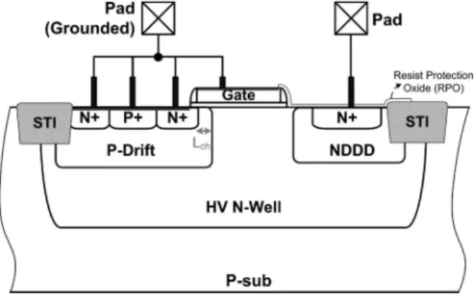
Fig. 1. Device cross-sectional view of the n-channel LDMOS in an 18-V BCD process.
line (T-line) through an HV power supply and then discharges the precharged energy into the device under test (DUT). T-line of a TLP system is equivalent to an impedance-matched capac-itor, which generates a square wave to stress the DUT. While gradually increasing the precharged voltage on T-line, TLP sys-tem is capable of measuring the snapback I–V characteristics of devices. Different from the 100-ns TLP system, a traditional curve tracer which sweeps a low-frequency voltage sine wave over the DUT can also measure the snapback I–V characteris-tics. The frequency of the sine wave is low enough, so that the curve-tracer measurement is considered as a dc measurement. At the same time, due to the long measurement duration, a curve tracer may damage the DUT particularly under the snapback
I–V measurement. Therefore, the holding voltages measured
from the 100-ns TLP are sometimes regarded as reference data to latch-up sensitivity in the IC industry.
In this letter, the holding voltages of an ordinary power-rail ESD protection device in HV CMOS ICs, the n-channel lateral DMOS (LDMOS), have been investigated by TLP systems with different pulsewidths and curve tracer. Transient latch-up (TLU) test was exploited to validate the measurement results.
II. DEVICESTRUCTURE
The device cross-sectional view of the n-channel LDMOS in a 0.25-µm 18-V bipolar CMOS DMOS (BCD) process is shown in Fig. 1. The clearance from drain contact to polygate edge and gate length (Lch) of the n-channel LDMOS are
optimized for ESD robustness. N-type double-diffused drain and P-Drift in Fig. 1 are lightly doped regions. Gate and source
CHEN et al.: INVESTIGATION ON THE VALIDITY OF HOLDING VOLTAGE IN HV DEVICES MEASURED BY TLP 763
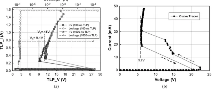
Fig. 2. I–V characteristics of the n-channel LDMOS measured by (a) 100- and 1000-ns TLP and (b) dc curve tracer.
electrodes of the n-channel LDMOS are shorted together through internal metal wiring. The n-channel LDMOS is laid out in finger type, with each finger width of 50 µm, and the total device width is 400 µm.
III. EXPERIMENTALRESULTS ANDDISCUSSION
Device secondary breakdown current (It2) measured by
TLP is usually adopted as a reference of ESD robustness. In order to approximate the device characteristics under human-body-model (HBM) ESD stresses, typical pulsewidth of TLP system is 100 ns [3]. The I–V characteristic of the n-channel LDMOS under 100-ns TLP measurement is shown in Fig. 2(a) (in square). Steps of the T-line precharge voltage are 0.5 V, and the TLP I/V are the averaged data of the measured current/ voltage waveforms from 50% to 90% of the pulse period. It2
of the n-channel LDMOS with a channel width of 400 µm is 1.5 A, and the corresponding HBM ESD robustness can be over the general requirement of 2 kV. From the 100-ns TLP measurement, the n-channel LDMOS shows a holding voltage of 11 V. However, distinct from the results of low-voltage devices, the holding voltage of n-channel LDMOS under curve-tracer measurement shows a substantial inconsistency to that measured by 100-ns TLP. As shown in Fig. 2(b), the holding voltage of n-channel LDMOS under curve-tracer measurement is 5.7 V only.
To investigate the huge Vhrolloff from 100-ns TLP (11 V)
to curve tracer (5.7 V), long-pulse TLP system with 1000-ns pulsewidth [4] was exploited. The long-pulse TLP system is capable of providing pulsewidths longer than 100 ns so that the time-domain device behavior of HV devices af-ter 100 ns can be further observed. As the measured result shown in Fig. 2(a) (in solid triangle), n-channel LDMOS under 1000-ns TLP has Vh of 9.1 V, which is lower than the Vh
under 100-ns TLP measurement but higher than the Vh
un-der curve-tracer measurement. The corresponding time-domain current and voltage waveforms of 1000-ns TLP measurement
Fig. 3. Time-domain waveforms of n-channel LDMOS under 1000-ns long-pulse TLP measurement.
are shown in Fig. 3, where perceptible degradation over time is observed.
From the Wunsch–Bell model, the simplified temperature model T (0, τ ) under the power source of a rectangular pulse with duration τ is T (0, τ ) = (q0/
√
πD)√t(t < τ ) [5]. As a
result, device temperature increases with time (t) during the duration of TLP pulses (τ ). In HV devices, the high device holding voltages can further accelerate the self-heating effect. With the increasing device temperature over time, β-gain of the parasitic bipolar inherent in n-channel LDMOS also increases. The holding voltage of n-channel LDMOS therefore degrades while the time increases, as the waveform shown in Fig. 3. From the measured voltage waveform, the self-heating speed of the LDMOS is found to be 1.5 V/µs. Extrapolating from the measured voltage waveform shown in Fig. 3 with the 1.5-V/µs self-heating speed, the time for n-channel LDMOS to reach Vh
of 5.7 V (that measured by curve tracer) is estimated as 3.2 µs. TLU test has been verified as an effective test method to evaluate the susceptibility of CMOS ICs to the latch-up induced
764 IEEE ELECTRON DEVICE LETTERS, VOL. 29, NO. 7, JULY 2008
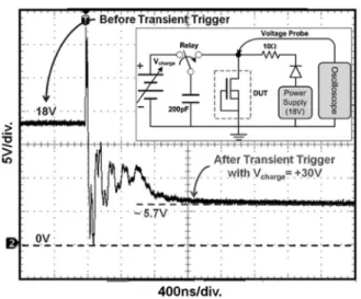
Fig. 4. Time-domain voltage waveform of n-channel LDMOS under TLU measurement with initial positive Vchargeof 30 V.
by transient noises in field applications [6]–[8]. The test setup for TLU is shown in the inset of Fig. 4. In the TLU test, the n-channel LDMOS was initially biased at normal circuit operat-ing voltage of 18 V. A transient noise is injected into n-channel LDMOS from the transient trigger source with precharged voltage Vcharge of +30 V. After the transient triggering, the
n-channel LDMOS was driven into latch-up state and clamped down the supply voltage. From the measured voltage waveform of TLU test shown in Fig. 4, the n-channel LDMOS clamped the supply voltage to∼5.7 V, which is the same value of Vh
under curve-tracer measurement. Moreover, time for n-channel LDMOS to clamp the supply voltage into a steady state is roughly around 1000 ns, whereas the voltage at 1000 ns under 1000-ns TLP measurement in Fig. 3 is∼9 V. In consequence, the TLU test has obviously verified that the TLP system over-estimates the holding voltage of an HV device, which in turn could underestimate its susceptibility to latch-up.
IV. CONCLUSION
The holding voltage of n-channel LDMOS in an HV BCD process has been investigated by TLP measurements with dif-ferent pulsewidths and dc curve tracer. It is found that the holding voltages of an 18-V n-channel LDMOS measured by 100-ns TLP system and curve tracer are substantially different, 11 and 5.7 V, respectively. The self-heating effect which de-grades the holding voltage of n-channel LDMOS over time has been observed. By using the long-pulse TLP, the self-heating speed of the HV transistors can be quantitatively estimated, where the 1.5-V/µs self-heating speed has been found in this letter. TLU test further verifies that TLP systems overestimate the holding voltage of n-channel LDMOS and underestimate its susceptibility to latch-up. As a result, TLP measurement is not suitable for applying to investigate the holding voltage of HV devices for latch-up, whereas the latch-up event is a reliability test with the time duration longer than milliseconds.
REFERENCES [1] S. Voldman, Latchup. New York: Wiley, 2007.
[2] M.-D. Ker and K.-H. Lin, “The impact of low-holding voltage issue in high-voltage CMOS technology and the design of latchup-free power-rail ESD clamp circuit for LCD driver ICs,” IEEE J. Solid-State Circuits, vol. 40, no. 8, pp. 1751–1759, Aug. 2005.
[3] T. Maloney and N. Khurana, “Transmission line pulsing techniques for circuit modeling of ESD phenomena,” in Proc. EOS/ESD Symp., 1985, pp. 49–54.
[4] M.-D. Ker and T.-X. Lai, “Dependence of layout parameters on CDE (cable discharge event) robustness of CMOS devices in a 0.25-µm salicided CMOS process,” in Proc. IEEE Int. Rel. Phys. Symp., 2006, pp. 633–634. [5] D.-L. Lin, “Thermal breakdown of VLSI by ESD pulses,” in Proc. IEEE
Int. Rel. Phys. Symp., 1990, pp. 281–287.
[6] G. Weiss and D. Young, “Transient-induced latchup testing of CMOS integrated circuits,” in Proc. EOS/ESD Symp., 1995, pp. 194–198. [7] M.-D. Ker and S.-F. Hsu, “Physical mechanism and device simulation
on transient-induced latchup in CMOS ICs under system-level ESD test,”
IEEE Trans. Electron Devices, vol. 52, no. 8, pp. 1821–1831, Aug. 2005.
[8] M.-D. Ker and S.-F. Hsu, “Component-level measurement for transient-induced latchup in CMOS ICs under system-level ESD considerations,”