國
立
交
通
大
學
材料科學與工程學系
碩
士
論
文
中尺寸薄膜電晶體液晶顯示器因 COG 封裝所造成局部
翹曲及應力對漏光現象之探討
Effects of Localized Warpage and Stress on
Chip-on-Glass Packaging Induced Light Leakage
Phenomenon in mid-size TFT-LCD
研 究 生:張晉誠
指導教授:呂志鵬 博士
中尺寸薄膜電晶體液晶顯示器因 COG 封裝所造成局部翹曲及應力 對漏光現象之探討
Effects of Localized Warpage and Stress on Chip-on-Glass Packaging Induced Light Leakage Phenomenon in mid-size TFT-LCD
研 究 生:張晉誠 Student:Chin-Cheng Chang
指導教授:呂志鵬 Advisor:Dr. Jihperng Leu
國 立 交 通 大 學 材 料 科 學 與 工 程 學 系
碩 士 論 文
A Thesis
Submitted to Department of Materials Science and Engineering College of Engineering
National Chiao Tung University in partial Fulfillment of the Requirements
for the Degree of Master
in
Materials Science and Engineering July 2009
Hsinchu, Taiwan, Republic of China
中尺寸薄膜電晶體液晶顯示器因 COG 封裝所造成局部翹曲及應力 對漏光現象之探討 學生:張晉誠 指導教授:呂志鵬 博士 國立交通大學 材料與工程學系碩士班
摘 要
漏光Mura 是指在液晶顯示器(LCD)面板上亮度不均勻的瑕疵。此缺陷源自 於Chip-on-Glass (COG) 封裝,由於玻璃基板和矽晶片之間熱膨脹係數的差異, 當矽晶片藉由異方性導電薄膜(ACF)與玻璃基板黏合,將會使面板產生翹曲進而 導致漏光Mura 發生。如今為了滿足顯示器輕量化的需求而使用更薄的玻璃基板 將使得漏光Mura 缺陷更加嚴重。 本論文利用商用模擬軟體 ANSYSTM以有限元素分析法(FEA)建立一 3D 數 值模型來計算 LCD 面板在經過 COG 封裝之後所產生的翹曲及應力,並研究其 與漏光現象的相關性,進而探討 COG 封裝所引起之 Mura 缺陷的成因。接著研 究製程溫度及 ACF 的材料性質還有矽晶片的尺寸大小及排列對 Mura 缺陷的影 響。此外利用量測表面形貌儀器KOSAKA ET4000A,藉由實際的實驗量測來驗 證模擬的可靠度。 根據實驗及模擬計算的結果,發現了面板翹曲、應力分佈和漏光現象之間具 有高度的相關性。根據分析結果探討可能造成漏光缺陷的根本原因,主要是由於液晶分子的指向矢及在配向膜表面的分子鏈排列方向會被COG 封裝所產生的應 力所影響而造成。雖然LCD 為了輕薄化而將玻璃基板厚度從 0.5 mm 降至 0.3 mm 時會產生漏光現象,但藉由將製程溫度由 180 oC 降至 160 oC 及採用低楊氏模數 的 ACF 可以將漏光缺陷有效改善或消除。最後本論文提出其它改善漏光現象的 方法,例如使用薄化的矽晶片、縮減矽晶片的長度或填充材料(dummification)等 方式,並且利用數值模擬來計算其改善漏光的效率。這些方法不僅具有低本成及 高可行性的優勢,從模擬計算結果來看還可以有效解決 Mura 漏光缺陷。
Effects of Localized Warpage and Stress on Chip-on-Glass Packaging Induced Light Leakage Phenomenon in mid-size TFT-LCD
Student: Chin-Cheng Chang Advisor: Dr. Jihperng Leu
Department of Materials Science and Engineering National Chiao Tung University
Abstract
Light leakage Mura i.e. the non-uniform brightness in LCDs, occurred upon the completion of chip-on-glass (COG) packaging of silicon IC drivers through the thermal bonding of anisotropic conducting film (ACF) resulting from the coefficient of thermal expansion (CTE) mismatch between glass substrate and silicon chips. Mura defect deteriorated as thinner glass plates were introduced to meet market demand for light weight and high mobility in mid-size TFT-LCD.
In this study, a 3-D finite element analysis (FEA) model using ANSYSTM was first established to examine the warpage and stress behavior of the glass substrate in order to explore their correlation with light leakage phenomenon. In addition, the simulated warpage data were validated by surface contour measurement tool using surface profiler, KOSAKA ET4000A. Specifically, the root-causes of Mura defect induced by COG package were examined and proposed. Then, the impact of thermal bonding temperature and thermo mechanical properties of ACF on Mura defect was investigated. In addition, the effects of dimension and layout of Si chips were also explored.
Based on experimental data and numerical analysis, a strong relationship among light leakage defect, warpage and stress behavior has been established. Besides, the root-causes of light leakage phenomenon were proposed. The Mura may result from the re-orientation of the director of the liquid crystal molecules and/or the orientation of the polymer chains on the alignment layer surface induced by the non-uniform stress resulting from COG packaging. Although the light leakage Mura appeared when the thickness of glass substrate was decreased from 0.5 mm to 0.3 mm, reducing ACF thermal bonding temperature from 180 to 160 oC or reducing ACF modulus can effectively eliminate Mura defect. Numerical modeling was also utilized to analyze the effectiveness of the dimension and layout of Si chips on Mura improvement. A low cost and effective solution can be achieved through thin silicon die, shorter die in length or the use of dummification.
Acknowledgements
轉眼間兩年的碩士生涯即將結束,在這段日子中,特別要感謝我的父母張耕 山先生及李秀枝女士在背後默默的全力支持,使我可以在無後顧之憂之下順利完 成學業。也非常感謝姊姊雅惠,在我的日常生活上也給予很大的協助。 感謝指導教授呂志鵬老師的協助使本論文得已臻於完善。在碩士求學期間不 厭其煩的教導及觀念上的糾正,使我在學術研究方面有長足的進步。不論是在研 究態度上或是處事方面都從老師那學到了很多經驗,獲益良多。 感謝實驗室的學長姐們,特別是國原學長在學問及生活方面上都不吝給予建 議;欣源學長,教導我模擬的啟蒙老師;牧龍學長在實驗上的協助;昱涵學長、 幸鈴學姐、泰印學長、明義學長、王智學長、弘恩學長、柏村學長的熱心指導, 因為有你們的協助才使得本論文能順利的完成。感謝伯政學弟、瑜修學弟、琬婷 學妹,還有我兩位要好的同學,茹瑛和詩雅在這段不算短的日子中一同打拼一起 成長。 最後我要感謝我最重視的人,珮齡。在這些日子中,當我有挫折或不如意時, 因為你的鼓勵才能讓我重新振作,感謝你長時間以來的關懷及照顧,有你的陪伴 對我來說是最幸福的事。謹以此文獻給我最親愛的你。 感謝奇美電子公司對此研究的經費支持。 張晉誠 國立新竹交通大學 民國九十八年七月Contents
摘 要...i
Abstract... iii
Acknowledgements ...v
Contents ...vi
Table Captions... viii
Figure Captions...ix
Chapter 1 Introduction...1
1.1 Background ...1
1.2 Overview ...4
2.1 Thin Film Transistor Liquid Crystal Display (TFT-LCD)...5
2.1.1 TFT-LCD Structure ...5
2.1.2 Working Principle of TFT-LCD ... 11
2.2 Chip-on-Glass (COG) Package...12
2.3 Anisotropic Conductive Film (ACF) ...13
2.3.1 Structure of Anisotropic Conductive Film...14
2.3.2 Principle of ACF electrical conductivity ...16
2.3.3 Issues of the ACF-typed COG Package...16
2.4 Mura Defects in TFT-LCDs ...17
Chapter 3 Finite Element Analysis and Experimental ...20
3.1 Finite Element Analysis (FEA) Method ...20
3.1.1 Introduction of FEA ...20
3.1.2 Theory of Linear Elastic Deformation ...21
3.2 Setup of Numerical Model Setup...30
3.2.1 COG Processes and Problem Statements...30
3.2.2 Selected Elements...30
3.2.3 Assumptions of FEA Model...33
3.2.4 Transient Thermal Analysis Model ...34
3.2.5 Warpage Analysis Model ...35
3.3 Experimental Measurement of Warpage ...39
Chapter 4 Results and Discussion ...41
4.1 Thermal Transient Analysis ...41
4.2 Warpage Analysis...44
4.3 Stress Analysis ...53
4.4 The Root-Causes of COG-Induced Mura in LCD ...55
4.4.1 Liquid Crystal Molecules ...55
4.4.2 Alignment Layer...57
4.5 Effect of the Thickness of Glass Substrate, Properties of ACF and Layout of Si chips on Mura Defects ...59
4.5.1 Thickness of Glass Substrate ...59
4.5.2 Bonding Temperature, Modulus and CTE of ACF...62
4.5.3 Dimensions and Arrangement of Si chips...71
Chapter 5 Conclusions...82
Table Captions
Table 3.1 Material properties for transient thermal analysis...35
Table 3.2 Geometry dimensions of components in simulation models ...38
Table 3.3 Material properties of components for thermal mechanical analysis...38
Table 3.4 Temperature-dependent Young’s modulus of ACF and LCD sealant ...38
Table 4.1 Localized warpage from outside to central of LCD panel in different sample conditions ...68
Table 4.2 Maximum localized warpage and 1st principle stress corresponding to specific conditions with 0.3mm glass substrate ...81
Figure Captions
Figure 1.1 Schematic illustration of warpage induced after ACF thermal bonding ...3
Figure 1.2 Light leakage Mura in TFT-LCD ...3
Figure 2.1 Schematic illustration of LCD assembly...5
Figure 2.2 Cross-section view of schematic illustration of backlight...6
Figure 2.3 Cross-section view of schematic illustration of cell structure...6
Figure 2.4 Schematic illustration of the TFT pixel unit...7
Figure 2.5 Color filter array in TFT-LCD...8
Figure 2.6 showed a schematic illustration of polarizer working principle...9
Figure 2.7 Simplified representation of rubbing...10
Figure 2.8 (a) Berreman model of alignment and (b) molecular model of alignmen..11
Figure 2.9 Schematic illustration of the operation principle in twisted nematic (TN) cell ...12
Figure 2.10 Schematic illustration of COG package process ...13
Figure 2.11 Application of ACF adhesive...14
Figure 2.12 Schematic illustration of ACF structure ...15
Figure 2.13 Components of conductive particle in ACF ...15
Figure 2.14 Schematic illustration of ACF conduction ...16
Figure 3.1 schematic illustration of stress vector... 22
Figure 3.2 Geometry of SOLID70 element ...31
Figure 3.3 Geometry of SOLID45 element ...32
Figure 3.4 Geometry of SOLID-SHELL190 ...32
Figure 3.5 The normalized maximum deflection as a function of number of elements per edge for SolidShell190 and Solid185 ...33
Figure 3.6 A 3-D FEA model with 1/2 symmetry...37
Figure 3.7 Warpage of TFT-LCD panel as a function of elements number in FEA model ...39
Figure 3.8 Surface contour measurement tool, KOSAKA ET4000...40
Figure 4.1 Temperature distribution of Si-chip after 10s thermal bonding... 42
Figure 4.2 Cross section view of the thermal distribution...42
Figure 4.3 Transient thermal analysis of ACF temperature in 10s ...43
Figure 4.4 (a) Warpage profile of upper glass plate along x-axis near COG packaging and (b) schematic illustration of LCD global model...45
Figure 4.5 Plots of experimental data vs. simulation data for various conditions: (a) 180 oC/0.3 mm, (b) 170 oC/0.3 mm, (c) 160 oC/0.3 mm, (d) 180 oC/0.5 mm, (e) 180 oC/0.5 mm and (f) 180 oC/0.5 mm ...49
Figure 4.6 Surface topography of 180oC / 0.3mm TFT-LCD panel which described in (a) experimental measurements and (b) computer simulation ...51
Figure 4.7 Surface topography of 160oC / 0.3mm TFT-LCD panel which described in experimental measurements...52
Figure 4.8 Pictures of light leakage phenomenon with ACF bonding temperature at (a) 180oC and (b) 160oC...52
Figure 4.9 The stress distribution curve along the bottom edge of the glass substrate53 Figure 4.10 Maximum principle stress distribution contour in LCD glass substrate in 1/2 symmetric model ...54
Figure 4.11 Schematic illustration of root-cause of Mura by liquid crystal reorientation...56
Figure 4.12 Schematic illustration of polymer chains near surface reorientated due to shear stress ...58 Figure 4.13 Maximum localized warpage and first principal stress as a function of
thickness of glass substrate with 180oC ACF bonding temperature...60 Figure 4.14 Photographs of lighted-up LCD panel with (a) 0.3 mm, and (b) 0.5 mm
glass substrate with 180oC ACF bonding temperature ...61 Figure 4.15 A plot of maximum localized warpage and first principal stress as a
function of ACF bonding temperature using 0.3mm glass substrate ...63 Figure 4.16 Photographs of lighted-up LCD panels with ACF bonding temperature at
(a) 180 oC and (b) 160 oC using 0.3 mm glass substrate ...64 Figure 4.17 A plot of maximum localized warpage and maximum first principal stress
as a function of ACF modulus with conditions of 180 oC / 0.3 mm ...66 Figure 4.18 Photographs of lighted-up LCD panels with (a) original ACF modulus
and (b) lower modulus under conditions of 180 oC/0.3 mm ...67 Figure 4. 19 The maximum localized warpage for different conditions...71 Figure 4.20 The maximum localized warpage as a function of dimensions of Si chip72 Figure 4. 21 Stress distribution profile between two adjacent chips at the edge (y=0
plane) for different shrinking percentage of chip’s length...74 Figure 4. 22 The maximum localized warpage as a function of Si chips placement...75 Figure 4.23 Schematic illustration of dummification ...76 Figure 4. 24 Simulation results of (a) warpage profile and (b) stress distribution for
conventional COG and dummification...77 Figure 4.25 The maximum localized warpage comparison of different (a) Young’s
Chapter 1 Introduction
1.1 Background
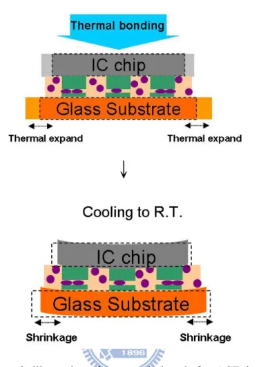
Thin film transistor liquid crystal displays (TFT-LCDs) have been widely used in TVs and monitors for computes, notebooks and hand-held devices. As the demand of LCD package moving towards ultra-thin package, chip-on-glass (COG) package offers the benefits of low-cost, high packaging density, and high pitch precision compared to the conventional package. In the processes of COG package, however, IC drivers are directly mounted on the glass substrate through anisotropic conductive film (ACF) attachment by thermal bonding, in which the mismatch of thermal expansion coefficient (CTE) between the Si chip and glass may induce large stress resulting in warpage as illustrated in Figure 1.1 and/or delamination [1,2]. Thus, the reliability and thermo-mechanical integrity of multilayered structure such as glass/liquid crystal/glass or Si/ACF/glass are the major concerns for COG packaging.
In the notebook market, the trend is moving towards large screen (larger than 10 inches) with ultra-thin and light-weight glass substrate. When the thickness of glass substrate was reduced from 0.5 mm to 0.3 mm and the panel size was increased from 10 to 13.3 inches, Mura defect involving non-uniform brightness in LCD, became severe for a 13.3” TFT-LCD with COG package using 8 IC drivers as shown in Figure 1.2. The light leakage phenomenon appeared only at the edge of LCD panel in half-moon-like shape. In addition, the region of light leakage was related to the IC drivers’ arrangement, appeared between Si chips. These practical observations showed the light leakage had highly relationship with the COG packaging.
The high temperature gradient during the ACF bonding process was reported to cause the warpage of glass substrate due to the CTE mismatch between glass substrate
and silicon-based chips [3,4]. Recently, Tsai et al. investigated the effects of the parameters such as thermal and moisture expansion of the ACF, and its elastic modulus and fillets on the warpage of ACF-bonded COG packages using a test structure (30x20x0.7 mm) [5]. It suggested that warpage of the COG package can be reduced by thermal cycling up to 85 oC and precisely controlling small CTE mismatch between chip and glass substrate, while insensitive to the bonding temperature. Chen et al reported that the light leakage was related to the thermal gradient and nonuniform stress distribution [6,7]. Nevertheless, the root-cause of the light leakage phenomenon in mid-size TFT-LCD panel caused by COG package has not been clearly addressed yet.
In this study, a 3-D finite element analysis (FEA) model was first established by ANSYSTM to examine the relationships among warpage, stress distribution and light leakage phenomenon in order to identify the root-cause of light leakage Mura. Furthermore, the analysis model was also used to explore the influence of various parameters of COG packaging such as thickness of glass substrate, bonding temperature, CTE and modulus of ACF on warpage and stress distribution in LCD panel. Finally, the impact of the layout and dimension of Si chips was analyzed by numerical modeling to explore possible low-cost solutions in eliminating Mura defect.
↓
Figure 1.1 Schematic illustration of warpage induced after ACF thermal bonding
1.2 Overview
The contents of this thesis were organized as following. In chapter 2, the background of LCD, COG package, ACF adhesive and Mura defect were first introduced. In chapter 3, the finite element analysis and experimental validation were described in detail. A 3-D finite element analysis (FEA) model coupled with transient thermal analysis using ANSYSTM was established. Next, in chapter 4, the results were studied to examine the warpage and stress behavior in COG package in order to explore the correlation with light leakage phenomenon. The root-causes of the light leakage phenomenon were related to the liquid crystal molecules and alignment layer. Furthermore, the effects of ACF bonding temperatures, thickness of glass substrate and material properties of ACF on light leakage Mura were studied. As a result, ACF bonding temperature was the most important parameter to recover the light leakage Mura which appeared when thickness of glass substrate decreased. The numerical models were also utilized to analysis and predict the effectiveness of solutions for improving light leakage phenomenon such as dimensions of Si chips and dummification. According to the results, shrinkage of height/length of Si chips and dummification can effectively eliminate light leakage Mura. Finally, conclusions were given in chapter 5 to summarize this work.
Chapter 2 Literature Review
2.1 Thin Film Transistor Liquid Crystal Display (TFT-LCD)
In order to respond the demands for light-weight, small volume and portability in flat panel displays, the liquid crystal display (LCD) was invented to replace the cathode ray tube (CRT) monitors. Thin film transistor liquid crystal display was a variant of liquid crystal displays which used thin film transistor technology to improve image performance such as brightness, contrast and low power consumption [ 8 ]. Nowadays, LCDs are widely used in television sets, computer monitors, notebooks, hand-held devices and personal digital assistants. The market of LCDs had increased tremendously in the recent years. [9]
2.1.1 TFT-LCD Structure
TFT-LCD had a sandwich-like structure with liquid crystal filled between two glass substrates as Figure 2.1 shown. [10]
The TFT-LCD mainly consisted of two parts, backlight system and cell. The backlight system was the light source of the LCD panel. The major components of backlight were an acrylic light pipe, the lamp usually placed at the end of the light pipe and the optical film and reflective film as shown in Figure 2.2. [11] Generally, these units of backlight were consisted to perform a uniform light. The cell part was mainly consisted of a TFT glass, a color filter glass, two polarizers attached to the glass substrate, liquid crystal and spacers filled between the two glass substrates as shown in Figure 2.3. [10]
Figure 2.2 Cross-section view of schematic illustration of backlight [11]
Figure 2.3 Cross-section view of schematic illustration of cell structure [10] Light pipe
Lamp
Light
Optical film
TFT-LCD was composed of complicate materials. The key parts were briefly described in the following:
1. TFT-array substrate:
TFT substrate was composed of millions TFT devices which was arranged as a matrix on an ITO substrate (Indium Tin Oxide, a transparent and electrical conductive material). Figure 2.4 showed a schematic illustration of a TFT pixel unit [12]. TFT manufacturing processes were similar to the lithography in semiconductor industry. The difference was that the TFT grown on a glass substrate, instead of silicon wafer. TFT was just like a switch which controlled the quantity of electrons into the capacitor. When enough electrons flowed into capacitor, the TFT device was shut down and the electrons kept in the capacitor. Therefore, TFT device can determine the strength of electrical field and then affect the orientation of the liquid crystal molecules. Each TFT pixel was operated independent, so that the bright or dark in each pixel can be controlled. Thus, the image can be shown on the screen.
2. Color filter substrate
The multi-color in TFT-LCD panels was attributed to the color filter array as Figure 2.5 shown [10]. Each pixel in TFT-LCD was subdivided into three sub-pixels, where one set of RGB sub-pixels was equal to one pixel. Because of the pixels were too small to distinguish, the color filter appeared to human eyes as a mixture of three colors. Each sub-pixel corresponded to a TFT unit which controlled the electrical field to determine the director of liquid crystal molecules, and then controlled the transparency of the light. Though the light only appeared in black or white (dark or bright) originally, a full-color was exhibited through the color filter.
Figure 2.5 Color filter array in TFT-LCD [10]
3. Polarizer
A polarizer was a film that converted an unpolarized or mixed-polarization beam of electromagnetic waves, e.g., light, into a beam with a single polarization state (usually a single linear polarization). Polarizers were used in many optical techniques
and instruments such as photography and liquid crystal display.
Figure 2.6 showed a schematic illustration of polarizer working principle [13]. A grid polarizer converted an unpolarized beam into one with a single linear polarization. The arrows depicted the electric field vector. The diagonally-polarized waves also contributed to the transmitted polarization. Their vertical components were transmitted, while the horizontal components were absorbed. TFT-LCD utilized the polarizer film to convert the light into polarized beam and controlled the light transparency.
Figure 2.6 showed a schematic illustration of polarizer working principle [13]
4. Alignment layer
The liquid crystal in TFT-LCD needed a method to induce uniform alignment of the liquid crystal molecules near the surface. The alignment layer coated on the glass substrate played the key role. Typically, the alignment layer used in LCD industry was polyimide due to its thermal stability for the application, in addition, cheap and easy to apply. The method of producing alignment layer included unidirectional rubbing of a spin-coated polyimide surface with a velvet cloth as Figure 2.7 shown [14]. Microgrooves were created and the polymer chains were aligned in a uniform direction on the polymer surface by the contact between polymer surface and cloth. The liquid crystal then interacted with such a surface and aligned in a unidirection.
The alignment mechanism of the rubbing process has been discussed for decades. The main ideas for alignment mechanism were roughly divided into two contributing components. One was a physical model, the liquid crystal molecules aligned with the microgrooves on the polymer surface. The other one was a molecular model which the factors for alignment was that molecular interactions between liquid crystal molecules and surface polymer chains. These two models were shown in Figure 2.8. The former model, physical one, was laid by Berreman, in his elastic continuum theory of 1972 [15]. This theory indicated that the liquid crystal molecules orient themselves parallel to the microgrooves. The driving force for this model was to minimizing the surface energy. The later model, molecules interactions one, was proposed by Geary in 1987. [16] The theory suggested that the polymer chain and/or substituents near the surface were aligned by the unidirectional rubbing. This results in that the surface polymer chain can interact with liquid crystal surface in a unidirectional alignment. Recent researches gave more agreement with the molecules interaction models. [17,18]
Figure 2.8 (a) Berreman model of alignment and (b) molecular model of alignment [15]
2.1.2 Working Principle of TFT-LCD
The inexpensive twisted nematic (TN) display was the most common type in TFT-LCD for notebooks. Figure 2.9 showed the schematic illustration of the operation principle in TN cell [19]. In TN cell, two linear polarizers attached on upper and bottom glass substrates were perpendicular to each other. When the nematic liquid crystal material was in the absence of an electrical field (OFF-state), the director of liquid crystal molecules at the top was perpendicular to the director at the bottom, twisted 90 degrees. The light entered the TN cell and its polarization state twisted with the director of the liquid crystal molecules. The light can transparent through the LCD cell appeared bright regions. On the contrary, when the LCD cell was in an electrical field (ON-state), the director of nematic liquid crystal molecules was parallel to the electric field direction and no longer twisted. Therefore, there was no light can transparent through the polarizer in regions where an electrical field was applied, appeared dark against the bright background.
Figure 2.9 Schematic illustration of the operation principle in twisted nematic (TN) cell [19]
2.2 Chip-on-Glass (COG) Package
Packaging technology of LCD IC drivers was an important process in LCD module. For improving the reliability and resolution of TFT-LCDs, the COG package had its benefits of low cost, high packaging density and potential for fine pitch compared to conventional package, for example, the tape automated bonding (TAB) packaging [20]. TAB was a process that places bare chips onto a printed circuit board (PCB) by attaching them to a polyamide film. Instead, COG technology which mounted the IC drivers on the glass substrate directly can save the cost of film substrate in TAB packaging. In the beginning, the COG technology was only applied to the small-sized display. Following the rapid progress of technique, the COG package technology also appeared in large-sized LCD (larger than 10 inches) to fulfill the requirements of high resolution, high I/O density, high performance and low-cost in package technology [21].
Figure 2.10 showed the schematic illustration of COG package process [22]. The IC drivers were directly mounted on the glass substrate by utilizing the anisotropic conductive film (ACF). The conductive particles in ACF deformed after applying temperature and pressure during a period of time, so that the bumps of IC drivers and the circuit on the glass substrate could be interconnected by the conductive particles.
Figure 2.3 Schematic illustration of COG package process [22]
2.3 Anisotropic Conductive Film (ACF)
Anisotropic conductive film was a conductive adhesive tape that had function of conducting electrically in vertical direction while completely insulating in horizontal direction. Besides, ACF tapes provided good mechanical adhesion between the IC drivers and various substrates such as glass, flexible plate and organic board. As Figure 2.11 shown, ACF were widely applied to chip-on-glass (COG), chip-on-film (COF), chip-on-board (COB), flexible-print-circuit (FPC), etc. [ 23 ] The ACF technology concerned to the IC driver package was especially important in LCD module. In addition, the requirement of fine pitch in IC drivers was decided by the properties of ACF such as conductive particle size and reliability.
ACF was mainly applied to the manufacturing processes which can not use the solder bump, for example, the inner circuit connects of LCD. Neither the outer lead
bonding (OLB) in TCP/COF package for LCD or the inner lead bonding (ILB) in COG for IC driver bonding, the ACF was the popular materials.
Figure 2.4 Application of ACF adhesive [23]
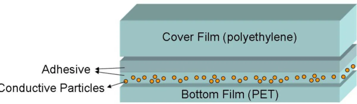
2.3.1 Structure of Anisotropic Conductive Film
Figure 2.12 showed the schematic illustration of ACF structure. ACF had conductive particles distributed randomly in adhesive matrix. The adhesive matrix usually adopted the thermal setting epoxy which had high temperature stability and low CTE as comparing to the thermal plastic epoxy. When the ACF underwent heat and pressure for a while, the compress stress of ACF had a good mechanical force to connect the two different materials. The advantages of ACF included: (1) ACF made as a tape which was easily fabricated, (2) the simplification of processes and equipment which did not require the reflow process and (3) uniform distribution of conductive particles can achieve high density pitch requirement.
Figure 2.5 Schematic illustration of ACF structure
The other important material in ACF was the conductive particles. Figure 2.13 showed the components of conductive particle which the polymer core was coated with Ni/Au. Polymer core can be treated as a buffer material for absorbing the stress induced by the thermal budget. Ni coated first due to Au had poor adhesion with the polymer core. Au had best ductility, little activity, which meant poor reactivity with other material, and good electrically conductivity that only weaker than silver and copper. The usual size of the conductive particle was 3-5 μm. Corresponding to the requirement of fine pitch in COG packaging, the design of the density and size of the conductive particles in ACF was very important. The small size conductive particles can prevent the electrical short in horizontal direction due to particles gathering.
2.3.2 Principle of ACF electrical conductivity
ACF was composed of conductive particles randomly dispersed in an insulator polymer matrix. When utilizing the ACF, cover film was ripped first and pasted on the substrate. Then ripped the other bottom film (PET) and bonded the electronic driver and substrate together after precisely alignment. By applying heat and pressure for appropriate time, the ACF film can provide good mechanical connects between IC drivers and substrate. Furthermore, ACF applied the vertical conducting electrically while insulating in horizontal as Figure 2.14 shown.
Figure 2.7 Schematic illustration of ACF conduction
2.3.3 Issues of the ACF-typed COG Package
The ACF-typed COG package had well-known problems about warpage and stress. The CTE mismatch among the ACF, chips and substrate was the main cause. The reliability of COG package concerned to the electrical short, contact resistivity increment and delamination. In particular, the delamination or crack at the interface of ACF and bumps was the most important issue. The warpage and deformation degree was related to the conductive resistance of the interconnection. The conductive resistance was lower at the center and input positions with larger deformation degree [24], and the outmost bump of IC driver usually had the most severity problems of
delamination and crack [25]. To solve the warpage and stress which were induced by ACF-typed COG package, it had been demonstrated that heating a glass substrate appropriately during COG interconnection and the use of a low stress type of ACF were very effective in reducing the warpage and improving the connection reliability in COG interconnection [26].
In addition, for the fine-pitched bump of IC drivers, fine pitch capability of ACF was desired especially in the COG package. The most important problem in fine-pitched IC was the electrical short in the horizontal direction since the conductive particles of ACF may easily trapped and form an electrical conduction in the small space of the adjacent bumps. Therefore, the size of conductive particles and the uniformity of distribution were important. Accordingly, the new typed ACF had double layer and conductive particles with insulate coated was proposed to improving the reliability of COG package [27]. Besides, the effects of height of bump and thickness of ACF were also reported that the different edged shapes of ACF had similar behavior and the warpage range would be enhanced with the ACF height [28].
2.4 Mura Defects in TFT-LCDs
The ACF-typed COG packaging may induce Mura defect. Nowadays, more than the improvement for LCDs manufacturing technology, the visual quality also became a potential issue. The front-of-screen quality is of considerable important for LCD performance for the costumers. The non-uniform of contrast, brightness and color in LCD were generally called “Mura”. Y. Mori et al reported the possible causes of Mura for TFT-LCDs as Table 2.1 listed [29]. The Mura was induced by many reasons due to the complicated structure and components of LCD panel. If there were problems in any of the manufacturing process, the Mura defect may occur. In this study, the type of Mura was classified to the light leakage Mura.
The visual performance of LCD had usually been evaluated by visual inspection. However, the Mura with low contrast was hard to inspect by a naked eye. The Mura can be characterized by using an original algorithm for uniformity extraction had been reported by Y. Mori et al [24]. Besides, different systems to quantitate the Mura were also reported [30,31,32,33].
Typically, the thermal stress was the major concern on the Mura defect of LCD TVs. The high temperature gradient caused by the backlight unit resulted in the warpage and stress concentration in LCD substrate. For solving the stress problem, Y. Shin et al. reported that by (1) Using glass with low photo-elastic coefficients to reduce stress-induce birefringence, (2) Reduction of heat stress on glass by means of change the configuration of compensation film of polarizer and (3) Improvement of spatial temperature variation of BLU (Back Light Unit) can improve the Mura on Diagonal Direction [34]. M. Lin et al. reported that the Mura was related to the ripple of the optical film which caused by the back light unit [35]. In addition, A. Ogasawaea et al. reported that the polarizer film shrinkage by heat and humidity, and improved the Mura by studying the adhesive with stress relaxation property [36]. However, the root-cause of the light leakage phenomenon in mid-size TFT-LCD panel caused by COG package has not been clearly addressed yet. The causes of the light leakage phenomenon will be discussed in the following chapter.
Table 2.1 Causes of Mura in TFT-LCDs [24]
Classification Causes
Cell
1. Nonuniform thickness of TFT array layer 2. Nonuniform density of liquid crystal 3. Nonuniform gap between glasses 4. Nonuniform color of color filter
Backlight
5. Nonuniform lamp rays 6. Wrinkled optical filter 7. Warped light pipe
Chapter 3 Finite Element Analysis and Experimental
The light leakage Mura in TFT-LCDs with COG packaging was found to be induced after ACF thermal bonding process to connect silicon IC drivers and wirings on the bottom glass. In this thesis, various manufacturing processes parameters of COG packaging (e.g. ACF curing temperature, CTE and modulus of ACF, and dimensions of COG packaging) were studied by a Finite-Element-Analysis package tool, ANSYSTM, to examine their effectiveness in reducing the warpage and thermal stress in LCD structure.
A brief introduction to the history of FEA and the basic theory of the numerical analysis will be given in this chapter. Moreover, the assumptions in this simulation and numerical model construction will be described in details. Finally, the experiment measurement for validating the simulation results will be also described.
3.1 Finite Element Analysis (FEA) Method
3.1.1 Introduction of FEA
In the beginning, the finite element method [37] was invented to investigate the complex elasticity and structural analysis problems in civil and aeronautic engineering. Its origin can be traced back to the research by Alexander Hrennikoff and Ricahrd Courant [38]. Development of the finite element method in the 1950s for airframe and structural analysis at University of Stuttgart through the work of John Argyris and at Berkeley through the work of Ray W. Clough in the 1960s for use in civil engineering [39]. The key concepts of stiffness matrix and element assembly used in today were established by late 1950s [40].
usually complex. For example, analyzing the deformation of a car in a crash, it is almost impossible to use only mathematical partial differential equations to describe and solve such a complicated problem. However, the finite element method can cut the complex structure into lots of small unit elements, and then the partial differential equations were created for each element which underwent an external force field. Based on the finite element method, each element pieced together and set the boundary conditions. Then the complex structural model for numerical analysis can be established. Finite element method allowed detailed visualization of where structures bend/twist and showed the distribution of stresses and displacements. Therefore, the engineers can construct, refine and optimize the whole design before manufacturing. Modern finite element method packages including components such as thermal, mechanic, elastic (or plastic) deformation analysis, electromagnetic and fluid has been well developed.
3.1.2 Theory of Linear Elastic Deformation [41]
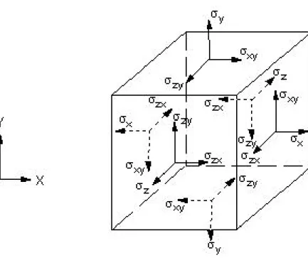
In this study, the COG packaging processes were analyzed by a FEA simulation tool, ANSYSTM, to investigate the deformation and stress distribution caused by the thermal bonding process. The materials used in this numerical model were assumed to be linear elastic. The relationship between stress and strain in linear elastic materials can be described by the Hook’s Law:
} ]{ [ } { el D ε σ = (3- 1) } { } { } {εel = ε − εth (3- 2) where:
} {σ = stress vector = T xz yz xy z y x ]
[σ σ σ σ σ σ , stress vector as Figure 3.1 shown ]
[D = elasticity or elastic stiffness matrix or stress-strain matrix }
{εel = elastic strain vector } {ε = T xz yz xy z y x ]
[ε ε ε ε ε ε , total strain vector }
{εth = thermal strain vector
Figure 3.1 schematic illustration of stress vector
Equation 3-1 may also be inverted to:
} { ] [ } { } {
ε
=ε
+ −1σ
D th (3- 3)T se z se y se x th T[ 0 0 0] } {
ε
=Δα
α
α
(3- 4) where: se xα = secant coefficient of thermal expansion in the x direction, if materials is isotropic, then se x α = se y α = se z α ref T T T = − Δ
T = current temperature at the point in question
ref
T = reference (strain-free) temperature
The flexibility or compliance matrix, [ ]−1
D is:
⎥
⎥
⎥
⎥
⎥
⎥
⎥
⎦
⎤
⎢
⎢
⎢
⎢
⎢
⎢
⎢
⎣
⎡
−
−
−
−
−
−
=
− xz yz xy z z yz z zx y yz y y yx x xz x xy xG
G
G
E
E
E
E
E
E
E
E
E
D
/
1
0
0
0
0
0
0
/
1
0
0
0
0
0
0
/
1
0
0
0
0
0
0
/
1
/
/
0
0
0
/
/
1
/
0
0
0
/
/
/
1
]
[
1υ
υ
υ
υ
υ
υ
(3- 5) where:Ex = Young's modulus in the x direction νxy = major Poisson's ratio
νyx = minor Poisson's ratio
If the material is isotropic, then:
Ex = Ey = Ez = E (3- 6)
νxy = νyx = νyz = νzy = νxz =νzx = ν (3- 7)
Gxy = Gyz = Gxz = G = E/2(1+ν) (3- 8)
Expanding Equation 3-3 with Equation 3-4 through Equation 3-8 and writing out the six equations below:
x z xz x y xy x x x x E E E T σ υ σ υ σ α ε = Δ + − − (3- 9) y z yz y y x x xy y y E E E T υ σ σ υ σ α ε = Δ − + − (3- 10) z z y y yz x x xz z z E E E T
υ
σ
υ
σ
σ
α
ε
= Δ − − + (3- 11) xy xy xy Gσ
ε
= (3- 12) yz yz yz Gσ
ε
= (3- 13) xz xz xz Gσ
ε
= (3- 14) where,εx = direct strain in the x direction σx = direct stress in the x direction εxy = shear strain in the x-y plane
σxy = shear stress on the x-y plane
Alternatively, Equation 3-1 may be expanded by Equation 3-5 and the combining that result with Equation 3-4 and Equation 3-6, 3-7 and 3-8 to give six equations below:
) )( ( ) ( ) ( ) ( ) ( 1 2 T h E T AB E E h E T E E h E z z xy yz xz z y y y z yz xz xy y x x y z yz x x Δ − + + Δ − + + Δ − ⎟ ⎟ ⎠ ⎞ ⎜ ⎜ ⎝ ⎛ − = α ε υ υ υ α ε υ υ υ α ε υ σ (3- 15) ) ( ) ( ) ( 1 ) ( 2 T E E h E T E E h E T E E h E z z x y xy xz yz z y y x z xz y x x y z yz xz xy y y Δ − ⎟⎟ ⎠ ⎞ ⎜⎜ ⎝ ⎛ + + Δ − ⎟⎟ ⎠ ⎞ ⎜⎜ ⎝ ⎛ − + Δ − ⎟ ⎟ ⎠ ⎞ ⎜ ⎜ ⎝ ⎛ + = α ε υ υ υ α ε υ α ε υ υ υ σ (3- 16)
(
)
) ( ) ( 1 ) ( ) ( 2 T E E h E T E E h E T h E z z x y xy z y y x y xy xz yz z x x xy yz xz z z Δ − ⎟⎟ ⎠ ⎞ ⎜⎜ ⎝ ⎛ − + Δ − ⎟⎟ ⎠ ⎞ ⎜⎜ ⎝ ⎛ + + Δ − + = α ε υ α ε υ υ υ α ε υ υ υ σ (3- 17) xy xy xyG
ε
σ
=
(3- 18) yz yz yzG
ε
σ
=
(3- 19) xz xz xzG
ε
σ
=
(3- 20) where, x z xz yz xy x z xz y z yz x y xy E E E E E E E E h=1−(υ )2 −(υ )2 −(υ )2 −2υ υ υ (3- 21)0 0 0 2 1 2 1 2 1 2 1 2 1 2 1 ε ε ε ε ε ε ε ε ε ε ε ε − − − z yz xz yz y xy xz xy x ] [ 1 2 3 0 ε ε ε ε = (3- 22)
Maximum strain difference εI:
] [ε1 ε2 ε2 ε3 ε3 ε1
εI = MAX − − − (3- 23)
The principal stress can be presented as σ0:
0 0 0 σ σ σ σ σ σ σ σ σ σ σ σ − − − z yz xz yz y xy xz xy x ] [ 1 2 3 0 σ σ σ σ = (3- 24)
Maximum stress difference σI:
] [σ1 σ2 σ2 σ3 σ3 σ1
σI = MAX − − − (3- 25)
3.1.3 Theory of thermal conduction and convection [25]
In this study, the thermal conduction and convection model were also employed. The first law of thermodynamics states that thermal energy is conserved. The first law of thermodynamics to a differential control volume can be describe as following:
q q L T L v t T c T ⎟+ T =&&& ⎠ ⎞ ⎜ ⎝ ⎛ + ∂ ∂ } { } { } { } { ρ (3- 26) where:
ρ= density c= specific heat T = temperature t = time ⎪ ⎪ ⎪ ⎭ ⎪ ⎪ ⎪ ⎬ ⎫ ⎪ ⎪ ⎪ ⎩ ⎪ ⎪ ⎪ ⎨ ⎧ ∂ ∂ ∂ ∂ ∂ ∂ = z y x L} { = vector operator = ⎪ ⎪ ⎭ ⎪⎪ ⎬ ⎫ ⎪ ⎪ ⎩ ⎪⎪ ⎨ ⎧ = z y x V V V v}
{ velocity vector for mass transport of heat
}
{q = heat flux vector q&&
& = heat generation rate per unit volume
Next, Fourier’s Law is used to relate the heat flux vector to the thermal gradients:
T L D q} [ ]{ } { =− (3- 27) where: ⎥ ⎥ ⎥ ⎥ ⎦ ⎤ ⎢ ⎢ ⎢ ⎢ ⎣ ⎡ = zz yy xx K K K D 0 0 0 0 0 0 ] [ = conductivity matrix
Kxx, Kyy, Kzz = conductivity in the element x, y and z directions, respectively
q T L D L T L V t T c T ⎟= T +&&& ⎠ ⎞ ⎜ ⎝ ⎛ + ∂ ∂ ) } ]{ ([ } { } { } { ρ (3- 28)
Equation 3-28 is then expand to its more familiar form:
⎟ ⎠ ⎞ ⎜ ⎝ ⎛ ∂ ∂ ∂ ∂ + ⎟⎟ ⎠ ⎞ ⎜⎜ ⎝ ⎛ ∂ ∂ ∂ ∂ + ⎟ ⎠ ⎞ ⎜ ⎝ ⎛ ∂ ∂ ∂ ∂ + = ⎟⎟ ⎠ ⎞ ⎜⎜ ⎝ ⎛ ∂ ∂ + ∂ ∂ + ∂ ∂ + ∂ ∂ z T K z y T K y x T K x q z T V y T V x T V t T c z y x z y x && &
ρ
(3- 29)It will be assumed that all effects are in the global Cartesian system. Three types of boundary conditions are considered, assuming that these cover the entire element.
1. Specified temperatures acting over surface:
T = T* (3- 30)
where T* is the specified temperature
2. specified heat flows acting over surface:
* } { } {q T η =−q (3- 31) where: }
{η = unit outward normal vector
*
q = specified heat flow
) ( } { } { f S B T T T h q η = − (3- 32) where: f h = film coefficient B
T = bulk temperature of the adjacent fluid
S
T = temperature at the surface of the model
Combining Equation 3-27 with Equations 3-30 and 3-31 yields the followings,
* } ]{ [ } {η T D L T =q (3- 33) ) ( } ]{ [ } { D L T hf TB T T = − η (3- 34)
Premultiplying Equation 3-28 by a virtual change in temperature, integrating over the volume of the element, and then combining with Equations 3-33 and Equation 3-34 with some manipulation yields:
∫
⎟ = ⎠ ⎞ ⎜ ⎝ ⎛ + ⎟ ⎠ ⎞ ⎜ ⎝ ⎛ + ∂ ∂ vol T T vol d T L D T L T L V t T T cδ { } { } { } (δ )([ ]{ } ) ( ) ρ∫
∫
∫
+ − vol S f BS2 Tq*d(S2) 3 Th (T T)d(S3) T&q&&d(vol) δ
δ
δ (3- 35)
where:
vol = volume of the element
T
3.2 Setup of Numerical Model Setup
3.2.1 COG Processes and Problem Statements
In order to investigate the effect of COG packaging on the light leakage phenomenon, a 3-D finite element analysis was employed to carry out the thermo-mechanical stress and warpage analysis of LCD panel by utilizing the FEA simulation tool, ANSYSTM. In this study, the commercial 13.3-inch LCD panel (TN type) with 8 silicon IC drivers connected to the wirings on glass substrate through ACF was first investigated. When the thickness of LCD glass substrate decreased from 0.5 mm to 0.3 mm, the light leakage phenomenon appeared, as illustrated previously in Figure 1.2. In this study, the light leakage region only appeared at the edge of LCD panel with COG packaging in half-moon-like shape and showed less severity near corners. Moreover, it was related to the Si chips arrangement, the light leakage showed between chips. According to the observations about the light leakage phenomenon, it was highly related with the COG packaging. Furthermore, the warpage and stress induced by COG packaging were analyzed by simulation tool to figure out the root-cause(s) of the light leakage Mura.
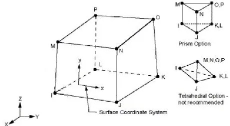
3.2.2 Selected Elements [25]
In this simulation model, the materials used in COG package were treated as elastic linear materials. Appropriate elements were selected for fitting the structure and materials characteristics in a LCD panel. 3-D element of SOLID70 was chosen for thermal analysis. Moreover, SOLID45 element and SOLID-SHELL190 element (for high aspect ratio) for 3-D model were chosen for mechanical analysis. A brief introduction to these elements is given below:
1. SOLID70
SOLID70 has a 3-D thermal conduction capability. The element has eight nodes with a single degree of freedom, temperature, at each node. The element is applicable to a 3-D, steady-state or transient thermal analysis. If the model equipped with the conducting solid elements, is also to be analyzed structurally, the element should be replaced by an equivalent structural element, such as SOLID45.
Figure 3.2 Geometry of SOLID70 element
2. SOLID45
SOLID45 is used for the 3-D modeling of solid structure. The element is defined by eight nodes having three degrees of freedom at each node: translations in the nodal x, y, and z directions. The element has plasticity, creep, swelling, stress stiffening, large deflection, and large strain capabilities.
Figure 3.3 Geometry of SOLID45 element
3. SOLID-SHELL190
SOLSH190 is used for simulating shell structures with a wide range of thickness (from thin to moderately thick). The element possesses the continuum solid element topology and features eight-node connectivity with three degrees of freedom at each node: translations in the nodal x, y, and z directions. Thus, connecting SOLSH190 with other continuum elements requires no extra effort. The element has plasticity, hyper-elasticity, stress stiffening, creep, large deflection, and large strain capabilities.
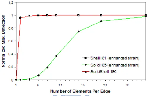
In addition, using SOLSH190 can acquire an accurate result even for the coarse meshes as shown in Figure 3.5. Besides, SOLSH190 element had benefits such as easy connection with other continuum elements, easy handling of variable thickness and no more need for mid-surface extraction.
Figure 3.5 The normalized maximum deflection as a function of number of elements per edge for SolidShell190 and Solid185
3.2.3 Assumptions of FEA Model
In order to obtain the balance between accuracy and efficiency, several assumptions are employed in this numerical model and summarized below:
1. All of the materials are isotropic and linear elastic due to the limited displacement in our model.
2. All of the components in the global model have perfect adhesion between each other.
3. The bumps underneath the Si chips are ignored due to their considerable quantities and limited effect on the thermal-mechanical deformation.
due to their limited influence on the thermal-mechanical deformation. 5. The global model is a 1/2 symmetric model
6. The symmetric surface is set as the symmetric plane, in which the translation and rotation are fixed.
7. The transient temperature distribution is calculated first, then applied to the thermal-mechanical model.
8. The temperature in third step of the warpage analysis was set at 25oC to simulate the cooling down process.
3.2.4 Transient Thermal Analysis Model
The thermal history of the COG packaging included a brief thermal bonding process (10 seconds typically) to curing the ACF adhesive and forming metal connection between Si chips and substrate. Due to the mismatch in material properties among Si chips, glass substrate and ACF adhesive, especially thermal conductivity and specific heat, a large thermal gradient existed in the COG assembly and resulted in the warpage and stress (localized and global). This was a non-steady state for thermal analysis since the global model was not in a thermal equilibrium state after only 10 seconds thermal bonding. Thus, a transient thermal was employed first to carry out the thermal distribution after the thermal bonding process. The LCD panel structure had a 1/2 symmetry, so only a 1/2 symmetric finite element model was established to enhance the simulation efficiency.
The selected element for the thermal analysis was SOLID70, which is a 3-D element with 8 nodes. An 180oC temperature thermal loading was applied to the top-side of the Si chips for 10 seconds. Also, the symmetric plane was set as the isothermal plane. In general, the heat transfer included three types: (1) thermal conductivity, (2) thermal convection, and (3) thermal radiation. However, it would take
up tremendous calculation time if all three types of heat transfer were taken into account. The specific values of thermal convection and thermal radiation needed the complex calculation through computational fluid dynamics (CFD). It was time consuming and not efficiency. Therefore, the experience formula of thermal transfer was applied to determine the thermal convection on the surface of the global model in this thermal analysis. Mulgaonker et al [42] and Chen et al [43] reported that by applying the thermal convection value of 8.5 W/m2 can obtain a certain accurate temperature distribution field in the model of small-sized assembly. Therefore, the value of thermal convection, 8.5 W/m2, was adopted in our model. Other material properties, for example, thermal conductivity, density and specific heat which used in this transient thermal model were obtained from literature and listed in Table 3.1. [28, 29]
Table 3.1 Material properties of the components in LCD for transient thermal analysis [28, 29]
Thermal conductivity(W/m-K) Density
(g/cm3) Specific heat (J/kg-。C) Glass substrate (Eagle2000) 1.5 2.370 710 Silicon chip 150 2.32 820 ACF 1.35 1 710 LCD sealant 1.35 1.2 710
3.2.5 Warpage Analysis Model
In order to investigate the effect of process parameters on light leakage phenomenon of the LCD panel, the model for thermal-mechanical stress and warpage
analysis was established by 3-D solid elements. The commercial 13.3-inch LCD panel was chosen to be the basic model in this study, 8 silicon chips as IC drivers were directly mounted on glass substrate through hundreds of bumps by thermal bonding of ACF near the panel edge. The panel structure included an ITO conductive film and optical films such as polarizer and compensation film, in addition to TN-based liquid crystal. To simplify the numerical model and reduce the computation time, the bumps, ITO and the optical films were not built in our model due to their limited influence on thermal-mechanical deformation. The model included components of glass substrate, Si chips, ACF adhesive and LCD sealant. The dimensions of all components were listed in Table 3.2. Since the LCD panel was a 2-fold symmetry, a 3-D model based on 1/2-panel was set up as shown in Figure 3.6. Because of a very high ratio (~1000) of length to thickness in both glass plates, a solid-shell element (Solid-Shell 190) was employed to obtain an accurate analysis [25]. The material properties of glass, Si chip, ACF adhesive and LCD sealant used in this model for thermal-mechanical analysis were listed in Table 3.3 [28, 29]. While the ACF and sealant were treated as temperature-dependent polymeric materials since they were sensitive to temperature as listed in Table 3.4. [44,45]
Taking into account of the thermal history of COG processing, the COG bonding process in this simulation was divided into three parts:
(1) The COG packaging was first carried out by applying high temperature and pressure on the topside of silicon chips to mount the chips onto bottom glass substrate through a bonding head. In the first simulation step, the global model was set at room temperature initially, and then a 180oC thermal loading was set on the top-side of the silicon chips and the z-axis displacement of chips was constrained due to the chips were held by bonding head and stage. Prior to thermal loading, the ACF was uncured and soft with very small elastic modulus as
compared to the silicon and the glass. Thus, the ACF were set as inactive elements.
(2) ACF was switched back to the active elements to simulate the curing process, while the temperature and constraint loading on silicon chips were still maintained in this step.
(3) The temperature and constraint loading on silicon chips were removed when the global model was cooled down to room temperature to simulate the COG-induced deformation behavior.
The symmetric constraint was applied on the symmetric plane. The back plane of the global model was constrained to avoid rigid motion. Moreover, a transient thermal analysis model which mentioned in the previous section was used to obtain the temperature distribution immediately after thermal bonding of ACF, for example at 180 oC. The temperature distribution at various locations was then applied to
aforementioned Step 1 and Step 2 as the boundary conditions to carry out the coupled thermal-mechanical analysis. Thus, the computation time can be significantly reduced.
Table 3.2 Geometry dimensions of components in simulation models Length (mm) Width (mm) Thickness (mm) Si chip 16.9 0.9 0.4 LCD sealant 146.5 1 3.875^10-3 ACF 146.5 1.1 25^10-3 Upper glass 146.5 184.55 0.3 Bottom glass 146.5 188 0.3
Table 3.3 Material properties of components for thermal mechanical analysis [28, 29] Young’s modulus
(GPa) Poisson ratio
CTE (ppm/oC) Tg( oC) Glass substrate (Eagle2000) 70 0.2 3.25 - Silicon chip 128 0.3 2.6 - ACF Table 3.4 0.4 CTE1=48.9 CTE2=168 119
LCD sealant Table 3.4 0.4 CTE1=68
CTE2=223 90
Table 3.4 Temperature-dependent Young’s modulus of ACF and LCD sealant [28, 29]
Temperature (。C) 21 100 150 190
ACF_Young’s modulus (GPa) 1.6 0.8 0.2 0.05
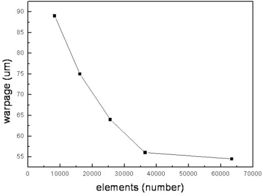
In FEA analysis, the mesh density decided the precision of the results. The more accurate result could be acquired by finer mesh but it would spend a lot of computation time. Therefore, the proper mesh density was examined in the beginning. Figure 3.7 shows the warpage of TFT-LCD panel as a function of elements number in our model. The warpage tended towards to certain value when elements number became large. The warpage difference between elements number of 36496 and 63390 was less than 2%. Thus, the mesh density chosen in our model was 36496 elements with 54502 nodes.
Figure 3.7 Warpage of TFT-LCD panel as a function of elements number in FEA model
3.3 Experimental Measurement of Warpage
To check the accuracy of the numerical model and analysis, the simulated warpage results were validated by surface contour measurement tool using KOSAKA ET4000A as shown by Figure 3.8. It was a probe system to measure the contour of the sample surface. The vertical resolution of this tool, KOSAKA ET4000A, was 0.1nm, which
vertical range was +/- 65um. It was appropriate for measurement of micro figure, step height, roughness and surface contour.
In order to explore the relationships between warpage and the light leakage phenomenon, surface contour measurement was carried out for measuring the warpage of the upper glass near the edge of LCD panel. The LCD panels for warpage measurement, which were supplied by Chi-Mei Optoelectronics Corp. (CMO), included various thickness of glass substrate (0.3 mm and 0.5 mm), different ACF bonding temperature (160 oC, 170 oC and 180 oC), and modulus of ACF (1.6GPa and 0.3 GPa at room temperature)
Chapter 4 Results and Discussion
4.1 Thermal Transient Analysis
Figure 4.1 shows the temperature distribution in one Si-chip after 10 seconds thermal bonding process at 180oC. Every Si chip on the LCD panel had the same temperature distribution due to the same treatment. Figure 4.2 shows the cross section view of temperature distribution across a LCD with COG package. The Si-chip and ACF reached 180 oC after the 10 seconds of thermal bonding. Immediately after thermal bonding, LCD sealant was ~90oC, which was still below its glass transition temperature. For a polymeric material at temperature below its Tg, the linear-elastic model was applicable to describe the thermal-mechanical behavior in general. Therefore, the sealant was treated as linear-elastic materials in this simulation model, instead of a plastic material, for the computational efficiency.
Figure 4.3 showed the transient thermal analysis of ACF (underneath Si chips) temperature in 10 seconds. The temperature of ACF reached 180oC in a very short time due to the high thermal conductivity of the Si chips with small dimension. In general, ACF needed to reach the 90% of the set temperature in 5 seconds to avoid the reflow of conductive adhesive arbitrarily.
Figure 4.1 Temperature distribution of Si-chip after 10s thermal bonding
Figure 4.2 Cross section view of the thermal distribution
a
a’
Si chip
178 178.5 179 179.5 180 1 2 3 4 5 6 7 8 9 10 Time (sec) Te m p. ( C )
4.2 Warpage Analysis
In the first stage, the commercial 13.3” TFT-LCD panel with original conditions of 0.3 mm glass substrate and 180 oC ACF curing temperature (0.3 mm/180 oC for simplifying for the rest of thesis) was studied. Based on surface contour measurement of upper glass along x-axis (parallel to the row of Si chips) at y =0 plane (see the coordinate system illustrated in Figure 3.5) shown in Figure 4.4(a), wave-like deformation induced by the silicon chips in COG package with a global warpage ~38 μm was found, while the localized warpage (valley to hilltop) was ~3.0 μm caused by the outmost chip (near A), and more severe, ~6.0 μm induced by the center chip (near B). The localized maximum warpage was found between two Si chips presumably due to the upward bending at Si chip edge.
(b)
Figure 4.4 (a) Warpage profile of upper glass plate along x-axis near COG packaging and (b) schematic illustration of LCD global model
Next, the validity of simulation model was examined by comparing the data of experimental and simulation as shown in Figure 4.5(a). Based on the results, the simulation data matched well with the experimental measurement. The global warpage was about 38 μm in both data and the location of the localized warpage induced by COG packaging also matched well in experimental data and simulation data. Figure 4.5(a) – 4.5(f) showed the experimental and simulation warpage data of LCD panel in various conditions of different ACF bonding temperatures (180 oC, 170 oC and 160 oC) and thickness of glass substrate (0.3 mm and 0.5 mm). The warpage
profiles from simulation in each case matched well with experimental surface topography in local warpage and global warpage. The difference of warpage profile between simulation and experimental data near the panel edge may arise from the pinning of polarizer attachment or glass substrate sealing in the LCD assembly. In contrast, perfect adhesion and little residual stress were assumed in our model.
The warpage induced by COG packaging was mainly caused by the thermal gradient and CTE mismatch in various components of LCD panel. In order to
B
A
symmetric surface z x y 0decrease the thermal gradient during the thermal bonding process, the simple and straightforward method was that decreasing the ACF bonding temperature. Once the ACF bonding temperature was decreased, the thermal gradient at the COG packaging region was decreased, and then the warpage was decreased simultaneously.
For 0.3 mm glass substrate, the warpage data of various ACF bonding temperature from 180 oC, 170 oC to 160 oC was illustrated in Figure 4.5(a)-(c). The global warpage from ~38 μm for 180 oC/0.3 mm case decreased to ~30 μm and ~15 μm in the condition of 170 oC/0.3 mm and 160 oC/0.3 mm. Not only the global warpage decreased with the lowering ACF bonding temperature, but the localized warpage induced by bending of Si chips decreased. The same trend also observed in the cases of 0.5 mm glass substrate as Figure 4.5(d)-(f) shown. However, the extent of the warpage in the cases of 0.5 mm glass substrate was all smaller than those cases of 0.3 mm glass substrate. Since the thicker glass substrate had ability to absorb more stress than thinner one did, the global warpage and localized warpage then both decreased.
(a)
Conditions: 180oC / 0.3mm
(b)
(c)
Conditions: 160oC / 0.3mm
(d)
(e)
Conditions: 170oC / 0.5mm (f)
Conditions: 160oC / 0.5mm
Figure 4.5 Plots of experimental data vs. simulation data for various conditions: (a) 180 oC/0.3 mm, (b) 170 oC/0.3 mm, (c) 160 oC/0.3 mm, (d) 180 oC/0.5 mm, (e) 180 oC/0.5 mm and (f) 180 oC/0.5 mm
Next, same contour measurement (along x-axis) was repeated from edge (y=0) to y=20 mm as shown in Figure 4.6(a). The global warpage (along x-axis) remained about the same (~38 μm), while localized warpage decreased at planes away from edge up to y=20 mm. It was observed that the wave-like deformation or localized warpage became indistinguishable at 15-20 mm from the edge in the y-direction, which coincided with the boundary of the light leakage region shown in Figure 2.16 from note book monitor. These results suggested that the light leakage phenomenon was related to the localized warpage which was caused by the bending of the silicon chips after COG packaging. The warpage profiles from simulation in Figure 4.6(b) matched well with experimental surface topography in local warpage and global warpage.
Figure 4.7 shows the warpage of 160oC/0.3mm case with repeated measurement from edge (y=0) to y=16 mm. The localized warpage also became indistinguishable when moved away from the edge. In this condition, however, the localized warpage disappeared at 12 mm-16 mm, where was closer to the edge than the condition of 180oC/0.3mm. Figure 4.8 shows the photos of LCD panels with 160 oC and 180 oC ACF bonding temperature in lighted-up state. The light leakage phenomenon was improved when the ACF bonding temperature was decreased from 180 oC to 160 oC. The region of light leakage at 160oC bonding temperature was smaller and the half-moon-like shape became not as clear as in the condition of 180oC bonding temperature. Again, these results suggested that the localized warpage had strong relationship with the light leakage phenomenon.
(a)
(b)
Figure 4.6 Surface topography of 180oC / 0.3mm TFT-LCD panel which described in (a) experimental measurements and (b) computer simulation
Figure 4.7 Surface topography of 160oC / 0.3mm TFT-LCD panel which described in experimental measurements
Figure 4.8 Pictures of light leakage phenomenon with ACF bonding temperature at (a) 180oC and (b) 160oC
![Figure 2.3 Cross-section view of schematic illustration of cell structure [10] Light pipe](https://thumb-ap.123doks.com/thumbv2/9libinfo/8050887.162389/19.892.187.708.800.1089/figure-cross-section-view-schematic-illustration-structure-light.webp)
![Figure 2.9 Schematic illustration of the operation principle in twisted nematic (TN) cell [19]](https://thumb-ap.123doks.com/thumbv2/9libinfo/8050887.162389/25.892.233.676.137.495/figure-schematic-illustration-operation-principle-twisted-nematic-cell.webp)
![Table 3.1 Material properties of the components in LCD for transient thermal analysis [28, 29]](https://thumb-ap.123doks.com/thumbv2/9libinfo/8050887.162389/48.892.155.738.716.983/table-material-properties-components-lcd-transient-thermal-analysis.webp)
![Table 3.3 Material properties of components for thermal mechanical analysis [28, 29] Young’s modulus](https://thumb-ap.123doks.com/thumbv2/9libinfo/8050887.162389/51.892.187.712.564.907/table-material-properties-components-thermal-mechanical-analysis-modulus.webp)