科技部補助專題研究計畫成果報告
期末報告
薄膜與二維系統之電子結構與拓樸態
計 畫 類 別 : 個別型計畫
計 畫 編 號 : MOST
104-2112-M-004-003-執 行 期 間 : 104年08月01日至105年12月31日
執 行 單 位 : 國立政治大學應用物理研究所
計 畫 主 持 人 : 楊志開
計畫參與人員: 博士後研究:李啟玄
報 告 附 件 : 出席國際學術會議心得報告
中 華 民 國 106 年 01 月 27 日
中 文 摘 要 : 由於不完全氫化,氫化石墨烯(石墨烷)的氫缺位會改變石墨烷的電
子結構,從而調制其電、磁及光學性質。我們有系統的以第一原理
電子結構計算研究石墨烷中的氫缺位團簇,這些分隔的團簇包括三
角形、平行四邊形、六邊形、及長方形等各種幾何形狀。結果發現
氫缺位會在純石墨烷的大能隙中產生新能階;所有三角形氫缺位團簇
均具有磁性,且面積越大磁矩越高;三角形及平行四邊形氫缺位能階
均自旋極化,且可應用於光躍遷;平行四邊形及開口型長方形氫缺位
團簇為反磁性,可應用於奈米級數位訊息登錄。
中 文 關 鍵 詞 : 石墨烯,石墨烷,氫缺位團簇,電子結構,磁性。
英 文 摘 要 : Hydrogen vacancies in graphane are products of incomplete
hydrogenation of graphene. The
missing H atoms can alter the electronic structure of
graphane and therefore tune the electronic, magnetic, and
optical properties of the composite. We systematically
studied a variety of well separated clusters of hydrogen
vacancies in graphane, including the geometrical shapes of
triangles, parallelograms, hexagons, and rectangles, by
first-principles density functional calculation. The
results indicate that energy levels caused by the missing H
are generated in the broad band gap of pure graphane. All
triangular clusters of H vacancies are magnetic, the larger
the triangle the higher the magnetic moment. The defect
levels introduced by the missing H in triangular and
parallelogram
clusters are spin-polarized and can find application in
optical transition. Parallelograms and openended rectangles
are antiferromagnetic and can be used for nanoscale
registration of digital information.
英 文 關 鍵 詞 : Graphene, graphane, hydrogen vacancy clusters, electronic
structures, magnetism.
www.nature.com/scientificreports
Electronic Structures of Clusters of
Hydrogen Vacancies on Graphene
Bi-Ru Wu1 & Chih-Kai Yang2
Hydrogen vacancies in graphane are products of incomplete hydrogenation of graphene. The missing H atoms can alter the electronic structure of graphane and therefore tune the electronic, magnetic, and optical properties of the composite. We systematically studied a variety of well-separated clusters of hydrogen vacancies in graphane, including the geometrical shapes of triangles, parallelograms, hexagons, and rectangles, by first-principles density functional calculation. The results indicate that energy levels caused by the missing H are generated in the broad band gap of pure graphane. All triangular clusters of H vacancies are magnetic, the larger the triangle the higher the magnetic moment. The defect levels introduced by the missing H in triangular and parallelogram clusters are spin-polarized and can find application in optical transition. Parallelograms and open-ended rectangles are antiferromagnetic and can be used for nanoscale registration of digital information.
Graphane is the end product of the complete hydrogenation of graphene1–20. Carbon atoms in graphane
are bonded to H atoms alternately from either side of the plane of graphene. Metal-insulator transition1–4
occurs as a result of the process, opening a large band gap6–11 for graphane. However, it is possible
that the hydrogenation process is not thorough and some H vacancies are left as defects in graphane. H vacancies in graphane are thus defined as C atoms not bonded to H. In a more controllable man-ner, some H atoms can desorb from one side of graphane as a result of an applied electric field12,13,20,
and the desorption process may continue to the extent of half hydrogenation. Patterns of H vacancies in graphane12–15,19,21–24 can thus be formed and have attracted considerable interests3,6,10–32 as partially
hydrogenated graphene or, equivalently, graphane with patches or clusters of H vacancies, can have very different electronic structure from either pristine graphene or graphane, providing almost unlimited ways for designing and fine-tuning electronic circuits based on the two-dimensional composite of C and H. In this article we would like to report investigations by density functional theory (DFT) on some geometric patterns of H vacancies in graphane and their physical properties. The results can be applied to the design of nanoelectronic circuits9–10,25 and may serve as a guide for predicting properties of larger and more
complicated patterns of the C-H composites.
H vacancies can be continuously distributed over a vast area and simulated by a large periodic struc-ture. H vacancies can also be confined in a finite area of graphane. Continuous presence of H vacancies can tune the width of band gap of graphane33,34 and, in the case of a single H-vacancy chain, even
turns the defected graphane into a conductor with linear band dispersion33 near the Fermi level. Locally
distributed H vacancies are more like quantum dots, offering essentially dispersionless defect states in the band gap. We chose a few geometric shapes of H-vacancy dots for calculation based on DFT. These highly symmetric clusters or dots of H vacancies serve as building blocks for more general and compli-cated patterns. Together with H-vacancy chains, they can be assembled for the design of a large variety of nanoelectronic circuits.
Starting with a cluster of four H vacancies as shown in Fig. 1a, we gradually enlarged the triangular dot to the one containing 121 vacancies in the process. Each equilateral triangle was placed in a large unit cell for DFT calculation to ensure its isolation from the triangles in adjacent cells. Relaxation of all atomic positions was always executed for the purpose of obtaining an optimal configuration with
1Department of Natural science, Center for General Education, Chang Gung University, Kueishan 333, Taiwan, ROC. 2Graduate Institute of Applied Physics, National Chengchi University, Taipei 11605, Taiwan, ROC. Correspondence and requests for materials should be addressed to C.-K.Y. (email: [email protected])
Received: 08 April 2015 Accepted: 21 September 2015 Published: 15 October 2015
OPEN
www.nature.com/scientificreports/
minimum stress before energy bands and other physical properties were calculated. One important result is the formation energy of individual H vacancies (Ef) defined as
= ( + ) + ( ) − ( )
( )
E E graphane HV E H E graphane
N 1
f total total total V
where Etotal(graphane + HV) is the total energy of graphane with the dot of H vacancies, Nv the
num-ber of H vacancies in the dot, Etotal(H) the total energy of Nv free H atoms, and Etotal(graphane) the
total energy of pure graphane. Alternate definition of the formation energy can be found in Part II of the Supplementary Information which accompanies this paper. Consistent with previous studies, larger spreading area of H vacancies lowers the energy needed to remove an outlying H atom. As Fig. 2a Figure 1. Configurations of H-vacancy clusters. (a–c) The triangular, parallelogram, zigzag-edged and
armchair-edged hexagonal H-vacancy dots are each built from the 4, 8, 6, and 12 C clusters and expanded to contain more C atoms. (d) Configuration of rectangular H-vacancy clusters. Blue and white circles represent C atoms belonging to two different sublattices. Inset of (a) is the complete configuration of a (green-shaded) triangular H-vacancy dot consisting of 4 C atoms (in black circles), with H atoms, some hidden behind C atoms, shown in light blue circles.
www.nature.com/scientificreports/
indicates, formation energy per H vacancy follows a decaying curve from 3.32 eV for the smallest triangle to less than 2.65 eV for those larger than 121 vacancies.
Also in decline as the H-vacancy dot grows larger is the band gap of the graphane containing the triangular dot, as is shown in Fig. 2b. The gap has its largest value at 1.56 eV for the smallest triangular dot and is reduced to less than 0.52 eV for the dot containing 121 vacancies. Figure 3a,b show two exam-ples of band structures for the smallest triangular vacancy dot and another with 36 vacancies. They all reveal essentially dispersionless spin-polarized energy bands in the graphane band gap. The flat bands are mostly made of pz orbitals contributed by the C atoms in either vacancy dot, with those corresponding
to the majority spin directly below the Fermi level and those of the minority spin above. For the larger dot, as Fig. 3b suggests, more spin-polarized flat bands appear in the valence and conduction bands, reflecting presence of more bare C atoms.
The triangular clusters of H vacancies are thus strongly associated with magnetism. As the fitted curve in Fig. 3c indicates, the total magnetic moment m of a triangular dot is practically proportional to the square root of the number of vacancies Nv the dot contains. The equation for the curve is m = .1 0094Nv0 4961.
in unit of μB. It allows design and construction of reliable nanoscale magnets on a two-dimensional
circuit. The enhancement of magnetism by the enlargement of vacancy clusters can be visualized by the plots of spin density in Fig. 4, in which the majority spin density greatly outnumbers the minority spin density in each configuration.
Our calculated magnetism for triangular H-vacancy clusters is also consistent with the discussion35,36
from the perspective of graphene with H adsorption. By considering the bare C atoms as distributed over a bipartite structure35 and C atoms of the same sublattice coupled ferromagnetically and those of different
sublattices coupled antiferromagnetically, one is able to obtain the same magnetic moment as given in the equation of the last paragraph for each of the triangular vacancy dot in Fig. 1a.
An H-vacancy cluster consisting of two back-to-back equilateral triangular dots has the shape of a parallelogram as shown in Fig. 1b and even number of H vacancies. Its distribution of magnetic moments is drawn in Fig. 5a for parallelograms consisting of the number of C atoms ranging from 18 to 72, in which two tips of any parallelogram have the largest but opposite moments. The other C atoms in the cluster have smaller moments depending on their spatial distances from the tips, with the C atoms at the edges of the cluster tending to shrink more slowly than those in the interior. Total magnetic moment is zero, which also agrees with the prediction based on the bipartite structure with equal number of bare C atoms distributed in two sublattices. The distribution of local moments, however, make the parallelogram an antiferromagnetic unit in which two quantum messages as represented by the opposite spins can be resolved within a few Å. If the two halves of the parallelograms are divided and separated by a single hydrogenated zigzag carbon line, as reported in Ref. 29, they are still coupled in antiferromagnetism.
From Fig. 2a, it is clear that for small and midsize (less than 70 C atoms) vacancy clusters, a paral-lelogram has smaller formation energy than that of a triangle containing the same number of C atoms. The reason is attributed to more exposed C atoms at the edges of the latter. Once the cluster grows large enough with comparable interior C atoms in both cases, the difference in formation energy is practically Figure 2. Formation energies and band gaps of H-vacancy clusters. (a) Formation energy of a vacancy
cluster generally falls with the enlargement of its size. (b) Band gap of a vacancy cluster shrinks as the cluster expands. Armchair-edged hexagonal dots are the exception.
www.nature.com/scientificreports/
erased. Band gaps of parallelograms also depend on their sizes, the larger the cluster the narrower the gap. The three band structures drawn in Fig. 5b correspond to the parallelogram dots of 8, 18 and 32 C atoms. Band gap shrinks abruptly from 2.02 eV for the cluster of 8 to 0.98 eV for the 18-C cluster. It rises slightly for the 32-C cluster but then conforms to the declining trend and eventually merges with curve for the triangles in Fig. 2b, consistent with our previous description of the parallelogram as a combina-tion of back-to-back triangles. The energy bands in Fig. 5b are not spin-split despite the sub-nanoscale distribution of spin density inside the cluster.
All hexagonal vacancy clusters are divided into two types that have either zigzag or armchair chains of edge C atoms as depicted in Fig. 1c. Left panel of Fig. 1c is illustration of zigzag-edge hexagonal dots starting from the smallest of 6 C atoms. Right panel of Fig. 1c shows the buildup of armchair-edged hex-agonal dots from 12 C atoms. For small hexhex-agonal dots, curves in Fig. 2a indicate that zigzag-edged ones have significantly lower formation energies. Small armchair-edged hexagonal dots need more energy to form because there are fewer nearest-neighbor H atoms in an armchair chain and it takes more energy to remove those H atoms to shape the edge. The difference in formation energy between the two types disappears for large hexagonal vacancy dots.
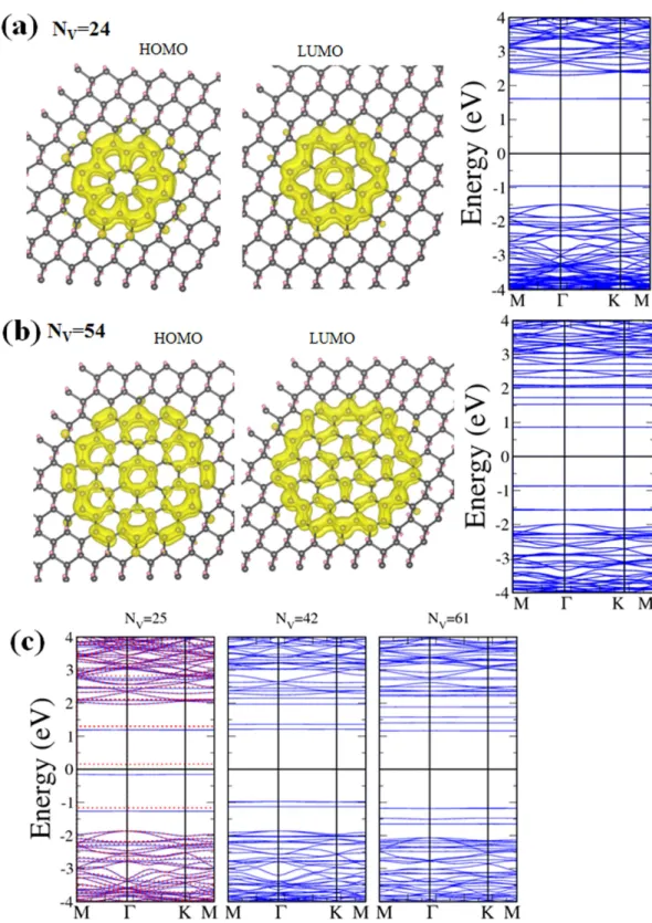
Band gaps of zigzag-edged hexagonal H-vacancy clusters follow a similar decaying curve shown in Fig. 2b as most other shapes, the larger the cluster the smaller the gap. However, energy gaps of hexag-onal clusters tend to be conspicuously higher than those of triangular or parallelogram clusters having comparable number of C atoms. In Fig. 6a,b two typical examples, one with 24 and another with 54 C atoms, are shown with their calculated band structures and charge densities at the highest occupied molecular orbital (HOMO) and lowest unoccupied molecular orbital (LUMO). Energy gap between the HOMO and LUMO drops from 2.56 eV for the cluster of 24 C atoms to 1.73 eV for the cluster of 54 C atoms, both close to the values reported in Ref. 30 for comparable configurations. It is also obvious that charge density for LUMO is more fragmented and has more nodes than that for HOMO in both Figure 3. Energy bands and magnetic moments of triangular H-vacancy clusters. (a) Energy bands along
symmetry directions for an H-vacancy cluster of 4 C atoms. Blue (red) curves are for the majority (minority) spin. (b) Same as (a) for a 36-C cluster. (c) Relationship between magnetic moment and number of C atoms in the vacancy cluster.
www.nature.com/scientificreports/
examples. No magnetism is associated with zigzag-edged hexagonal H-vacancy clusters. The clusters are all made of whole 6-member hexagonal rings and even number of C atoms in the bipartite structure. Local moments and therefore the total magnetic moment disappear.
No simple relation between the band gap and cluster size exists for armchair-edged hexagonal clus-ters. The smallest one (12 C atoms) has a similar band gap as those of the triangle and parallelogram with comparable number of C atoms. While larger hexagons have higher gaps, there is an exception for the one with 25 C atoms. This particular shape not only has the lowest band gap of only 0.31 eV but car-ries a magnetic moment of 0.742 μB with it. As the energy bands drawn in Fig. 6c reveal, only the 25 C
cluster has spin-polarized energy bands, with one dispersionless energy level belonging to the majority spin 0.15 eV below the Fermi level and another to the minority spin also only 0.15 eV above. The 25-C cluster is unique in possessing a magnetic moment in that it is the only armchair-edged cluster in Fig. 1C that simultaneously has broken hexagons and an uneven distribution of C atoms in the two sublattices.
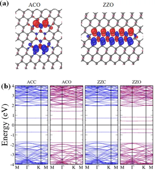
Finally we investigated rectangular H-vacancy dots. Four particular configurations were considered: zigzag-edged clusters with open or closed ends (ZZO or ZZC) and armchair-edged clusters with open or closed ends (ACO or ACC), depending on whether the dot contains only whole hexagons of C atoms. Figure 1d plots the four configurations and Fig. 7a displays the spin density in the two open-ended cases. Although both ACC and ZZC are made of closed hexagons and nonmagnetic, ACO and ZZO are asso-ciated with antiferromagnetism with zero total moment for each of the two clusters, in consistent with their more exposed and discontinuous configurations and even distribution of C atoms in the sublattices. It is also obvious that opposite magnetic moments concentrate on the two ends of ACO but spread out along the two edges of ZZO, making the two configurations shape-dependent nanoscale two-pole magnets. Energy bands for the four configurations are drawn in Fig. 7b, confirming the antiferromag-netic properties of the two open-ended structures as the bands corresponding to either spin overlaps. Figure 7b and Fig. 2b also indicate that ACO and ZZO have smaller band gaps than ACC and ZZC, with ZZO’s being the narrowest at 0.82 eV. The fact that both open-ended rectangular H-vacancy dots require more formation energies (Fig. 2a) than their close-ended counterparts is also quite as expected.
The various geometric shapes and sizes of H-vacancy dots we have studied provide a useful map for their application. Band gaps are generally consistent with the calculation of Gao et al.37, with one
exception of armchair-edged hexagonal vacancy dots. Where magnetism is concerned, triangular dots are good candidates for forming molecular magnets. By simply expanding the size equilaterally mag-netic moment increases in proportion to the square root of the number of C atoms contained inside. Spin-polarized energy levels near the Fermi level also make optical transitions and sensing31 available.
It is also possible to manipulate the optical transitions by making regular patterns of triangular dots32
segregated far enough from one another. Parallelograms have lower formation energies and are two-pole magnets, in sharp contrast to the triangles. Patterns of alternate presence of triangles, parallelograms, and Figure 4. Spin densities of triangular H-vacancy clusters. (a–e) Distribution of the majority spin (blue)
www.nature.com/scientificreports/
close-ended rectangles can be used to register digital information in very confined space. A hexagonal cluster tends to have the lowest formation energy but also the largest energy gap in most cases.
In summary, we have presented electronic structures and properties of a variety of H-vacancy clusters in graphane according to their geometric shapes and sizes. These vacancy dots, along with vacancy chains and ribbons, are useful building blocks for further research on related physics based on the platform of graphene. They can also be applied to the design of graphene-based microelectronic circuits.
Methods
We performed spin-polarized density-functional calculations using the Vienna ab initio simulation pack-age (VASP)38,39. For exchange-correlation functional, the version of Perdew, Burke and Ernzerhof40 was
adopted. The electron-ion interaction was represented by the projector-augmented wave potential. Cutoff energy for the expansion of wave functions and potentials in the plane-wave basis were chosen to be 500 eV. Complete relaxation of the combined structure including lattice constants was executed with a Figure 5. Spin densities and energy bands of parallelogram H-vacancy clusters. (a) Distribution of the
majority spin (blue) and minority spin (red) density within each of the four parallelogram dots. (b) Energy bands of the three parallelogram H-vacancy dots, containing 8 (left), 18 (middle), and 32 (right) C atoms respectively.
www.nature.com/scientificreports/
9 × 9 × 1 sampling of the first Brillouin zone. In our calculations, vacuum space in the supercell was allocated by setting a height of 15 Å perpendicular to the graphane plane in the cell, which proved large enough to minimize artificial interactions between supercells.
We have also adopted large unit cells in the calculation in order to accommodate various distributions of vacancy dots. A large unit cell containing 288 C atoms, for example, has been used for calculations involving large vacancy dots and for the testing of eliminating inter-dot interaction. All energy bands shown in the figures of this article are from calculations based on the unit cell of 128 C atoms.
Figure 6. Hexagonal H-vacancy clusters. (a) Charge densities of HOMO and LUMO and energy bands
for a hexagonal dot of 24 C atoms. (b) Same as (a) for a 54-C dot. (c) Energy bands for armchair-edged hexagonal dots containing 25 (left), 42 (middle), and 61 (right) C atoms respectively.
www.nature.com/scientificreports/
References
1. Elias, D. C. et al. Control of Graphene’s Properties by reversible hydrogenation: evidence for graphane. Science 323, 610–613 (2009).
2. Burgess, J. S. et al. Tuning the electronic properties of graphene by hydrogenation in a plasma enhanced chemical vapor deposition reactor. Carbon 49, 4420–4426 (2011).
3. Yin, W.-J., Wei, S.-H. & Yan, Y. Control of one-dimensional magnetism in graphene via spontaneous hydrogenation of the grain boundary. Phys. Chem. Chem. Phys. 15, 8271–8275 (2013).
4. Zhou, Y. et al. Hydrogenated graphene nanoflakes: semiconductor to half-metal transition and remarkable large magnetism.
J. Phys. Chem. C 116, 5531–5537 (2012).
5. Wang, Y. et al. Toward high throughput interconvertible graphane-to-graphene growth and patterning. ACS Nano 4, 6146–6152 (2010).
6. Haberer, D. et al. Tunable band gap in hydrogenated quasi-free-standing graphene. Nano Lett. 10, 3360–3366 (2010). 7. Sofo, J. O., Chaudhari, A. S. & Barber, G. D. Graphane: a two-dimensional hydrocarbon. Phys. Rev. B 75, 153401 (2007). 8. Lebègue, S., Klintenberg, M., Eriksson, O. & Katsnelson, M. I. Accurate electronic band gap of pure and functionalized graphane
from GW calculations. Phys. Rev. B 79, 245117 (2009).
9. Fiori, G. et al. Simulation of hydrogenated graphene field-effect transistors through a multiscale approach. Phys. Rev. B 82, 153404 (2010).
10. Balog, R. et al. Bandgap opening in graphene induced by patterned hydrogen adsorption. Nat. Matter. 9, 315–319 (2010). 11. Grassi, R., Low, T. & Lundstrom, M. Scaling of the energy gap in pattern-hydrogenated graphene. Nano Lett. 11, 4574–4578
(2011).
12. Sahin, H., Ataca, C. & Ciraci, S. Magnetization of graphane by dehydrogenation. Appl. Phys. Lett. 95, 222510 (2009). 13. Zhou, J. et al. Ferromagnetism in semihydrogenated graphene sheet. Nano Lett. 9, 3867–3870 (2009).
14. Feng, J. et al. Patterning of graphene. Nanoscale 4, 4883–4899 (2012).
15. Eng, A. Y. S. et al. Searching for magnetism in hydrogenated graphene: using highly hydrogenated graphene prepared via birch reduction of graphite oxides. ACS Nano 7, 5930–5939 (2013).
Figure 7. Rectangular H-vacancy clusters. (a) Spin densities of rectangular H-vacancy clusters ACO and
ZZO. Both are antiferromagnetic with local magnetic moments. (b) Energy bands for ACC, ACO, ZZC, and ZZO, from left to right.
www.nature.com/scientificreports/
16. Tang, Q., Zhou, Z. & Chen, Z. Graphene-related nanomaterials: tuning properties by functionalization. Nanoscale 5, 4541–4583 (2013).
17. Zhou, J., Wu, M. M., Zhou, X. & Sun, Q. Tuning electronic and magnetic properties of graphene by surface modification. Appl.
Phys. Lett. 95, 103108 (2009).
18. Su, W. S., Wu, B. R. & Leung, T. C. A first-principles study on the electromechanical effect of graphene nanoribbon. Comput.
Phys. Commun., 182, 99–102 (2011).
19. Tang, S., Yu, J. & Liu, L. Tunable doping and band gap of graphene on functionalized hexagonal boron nitride with hydrogen and fluorine. Phys. Chem. Chem. Phys. 15, 5067–5077 (2013).
20. Zhou, J. & Sun, Q. How to fabricate a semihydrogenated graphene sheet? A promising strategy explored. Appl. Phys. Lett. 101, 073114 (2012).
21. Berashevich J. & Chakraborty, T. Sustained ferromagnetism induced by H-vacancies in graphane. Nanotechnology 21, 355201 (2010).
22. Berashevich, J. & Chakraborty, T. Influence of adsorbates on the electronic and magnetic properties of graphane with H-vacancy defects. Phys. Rev. B 82, 134415 (2010).
23. Li, Y. & Chen, Z. Patterned partially hydrogenated graphene (C4H) and its one-dimensional analogues: a computational study.
J. Phys. Chem. C 116, 4526–4534 (2012).
24. Jones, J. D., et al. Formation of graphane and partially hydrogenated graphene by electron irradiation of adsorbates on graphene.
Carbon 48, 2335–2340 (2010).
25. Singh, A. K., Penev, E. S. & Yakobson, B. I. Vacancy clusters in graphane as quantum dots. ACS Nano 4, 3510–3514 (2010). 26. Huang, L. F. et al. Understanding the band gap, magnetism, and kinetics of graphene nanostripes in graphane. J. Phys. Chem. C
115, 21088–21097 (2011).
27. Dai, Q. Q., Zhu, Y. F. & Jiang, Q. Stability, electronic and magnetic properties of embedded triangular graphene nanoflakes. Phys.
Chem. Chem. Phys. 14, 1253–1261 (2012).
28. Wang M. & Li, C. M., Investigation of doping effects on magnetic properties of the hydrogenated and fluorinated graphene structures by extra charge mimic. Phys. Chem. Chem. Phys. 15, 3786–3792 (2013).
29. Wu, M., Wu X., Gao Y. & Zeng X. C. Patterned hydrogenation of graphene: magnetic quantum dot array. J. Phys. Chem. C 114, 139–142 (2010).
30. Cui, X. Y. et al. Quantification of graphene based core/shell quantum dots from first principles. Appl. Phys. Lett. 99, 183102 (2011).
31. Sun, H., Wu L., Wei W. & Qu X. Recent advances in graphene quantum dots for sensing. Mater. Today 16, 433–442 (2013). 32. Chuang, C. et al. Evidence for formation of multi-quantum dots in hydrogenated graphene. Nanoscale Res. Lett. 7, 459 (2012). 33. Wu, B. R. & Yang, C.-K. Electronic structures of graphane with vacancies and graphene adsorbed with fluorine atoms. AIP
Advances 2, 012173 (2012).
34. Wu, B. R. & Yang, C.-K. Energy band modulation of graphane by hydrogen-vacancy chains: a first-principles study. AIP Advances
4, 087129 (2014).
35. Yazyev, O. V. & Helm L. Defect-induced magnetism in graphene. Phys. Rev. B 75, 125408 (2007). 36. Niyogi, S. et al. Covalent chemistry for graphene electronics. J. Phys. Chem. Lett. 2, 2487–2498 (2011).
37. Gao X., Wei Z., Meunier V., Sun Y. & Zhang S. B. Opening a large band gap for graphene by covalent addition. Chem. Phys. Lett.
555, 1–6 (2013).
38. Kresse, G. & Furthmüller, J. Efficient iterative schemes for ab initio total-energy calculations using a plane-wave basis set. Phys.
Rev. B 54, 11169–11186 (1996).
39. Kresse, G. & Furthmüller, J. Efficiency of ab-initio total energy calculations for metals and semiconductors using a plane-wave basis set. Comput. Mater. Sci. 6, 15–50 (1996).
40. Perdew, J. P., Burke, K. & Ernzerhof, M. Generalized gradient approximation made simple. Phys. Rev. Lett. 77, 3865–3868 (1996).
Acknowledgments
This work was supported by the Ministry of Science and Technology of the Republic of China under grant numbers NSC 101-2112-M-004-004-MY3 and NSC 102-2112-M-182-002-MY3. Supports from the National Centers for Theoretical Sciences and High-performance Computing of the ROC are also gratefully acknowledged.
Author Contributions
B.R.W. and C.K.Y. planned and discussed the research. B.R.W. performed the calculations and C.K.Y. wrote the manuscript. Both discussed the results and contributed to the scientific interpretation as well as to the writing of the manuscript.
Additional Information
Supplementary information accompanies this paper at http://www.nature.com/srep Competing financial interests: The authors declare no competing financial interests.
How to cite this article: Wu, B.-R. and Yang, C.-K. Electronic Structures of Clusters of Hydrogen Vacancies on Graphene. Sci. Rep. 5, 15310; doi: 10.1038/srep15310 (2015).
This work is licensed under a Creative Commons Attribution 4.0 International License. The images or other third party material in this article are included in the article’s Creative Com-mons license, unless indicated otherwise in the credit line; if the material is not included under the Creative Commons license, users will need to obtain permission from the license holder to reproduce the material. To view a copy of this license, visit http://creativecommons.org/licenses/by/4.0/