IEEE ELECTRON DEVICE LETTERS, VOL. 23, NO. 5, MAY 2002 255
Anomalous Variations of OFF-State Leakage
Current in Poly-Si TFT Under Static Stress
Kow Ming Chang, Member, IEEE, Yuan Hung Chung, Student Member, IEEE, and
Gin Ming Lin, Student Member, IEEE
Abstract—In this letter, we study the anomalous variations of the
OFF-state leakage current( OFF) in n-channel poly-Si thin-film transistors (TFTs) under static stress. The dominant mechanisms for the anomalous OFFcan be attributed to 1) OFF increases due to channel hot electrons trapping at the gate oxide/channel in-terface and silicon grain boundaries and 2) OFF decreases due to hot holes accumulated/trapped near the channel/bottom oxide interface near the source region. Under the stress of high drain bias, serious impact ionization effect will occur to generate hot elec-trons and hot holes near the drain region. Some of holes will be in-jected into the gate oxide due to the vertical field( (V Gstress
V Dstress) OX) near the drain and the others will be migrated
from drain to source along the channel due to lateral electric field
( V Dstress CH).
Index Terms—OFF-state leakage current( OFF), impact
ion-ization, poly-Si TFT.
I. INTRODUCTION
P
OLY-Si TFTs have been greatly studied for applications in static random access memories (SRAMs) and active ma-trix liquid crystal displays (AMLCDs). Although the mobility of poly-Si TFTs is much higher than that of amorphous TFTs, the high OFF-state leakage currents in poly-Si TFTs are also unavoidable [1]. It has been reported that the OFF-state leakage currents can be attributed to the thermal generation effect at low gate-drain electric field and to the electric field effect at high gate-drain electric field in the channel [2], [3]. Several inves-tigations have been already carried out to study the ON-state degradation under static stress in poly-Si TFTs [4], [5]. How-ever, to our knowledge, the variations of the OFF-state leakage currents under static stress are not yet well defined. The object of this work is to study the anomalous variations of the OFF-state leakage currents in poly-Si TFTs under static stress. For-ward and reverse mode measurements are used for the OFF-state leakage currents in drain and source regions, respectively.II. EXPERIMENT
Low-temperature processed ( 600 C) n-channel poly-Si TFTs are used in this work. The physical device parameters are 56 nm-thick PECVD gate oxide deposited at 350 C,
Manuscript received August 28, 2001; revised January 30, 2002. This work was supported by the National Science Council, Taiwan, R.O.C., under Con-tract NSC90-2215-E009-039. The review of this letter was arranged by Editor T.-J. King.
K. M. Chang, Y. H. Chung, and G. M. Lin are with the Department of Elec-tronics Engineering and Institute of ElecElec-tronics, National Chiao-Tung Univer-sity, Hsinchu 300, Taiwan, R.O.C.
Publisher Item Identifier S 0741-3106(02)04099-5.
100 nm-thick active channel, channel width m,
and channel length m. The active channel was
deposited from the decomposition of Si H in LPCVD system at 460 C and then crystallized at 600 C for 24 h. The measured average grain size is 1.1 m. After completing the device fabrication, no hydrogenation step was performed.
In this letter, the static stress is used to degrade the poly-Si TFTs. The gate potential fixed at 20 V (
V) and the drain potential ranged from 20 V to 32 V
V– V). was measured at
V and V. Forward mode and reverse mode
mea-surements are used to characterize variations at the drain side and at the source side, respectively. In the forward mode, the source and drain connections are the same as during stress, while in the reverse mode, they are swapped.
III. RESULTS ANDDISCUSSION
Figs. 1 and 2 show the variations under forward mode and reverse mode measurements for
ranging from 20 V to 32 V, respectively. Insert plots are the – characteristics of poly-Si TFTs before and after static stress for forward mode and reverse mode measure-ments, respectively. Less variations can be observed at
V V, while anomalous variations can
be observed at V. For forward mode measurements
at V, is almost unchanged initially and
then increased after 100 s. This implied that the device was less degraded at the initial stage, while the increase of was due to the channel hot electrons trapped in the pre-existed traps (acceptor-like trap states) at the gate oxide/channel interface and silicon grain boundaries or due to the weak bonds (Si-H, distorted Si-Si, and distorted Si-O) broken caused by the channel hot electrons near drain. The trapped electrons at the interface increase the vertical electric field near drain to
increase [6]. However, for V in forward
mode measurements, increases at the initial stage and finally reaches saturation after 1000 s. The saturated is due to the increase of injection efficiency for hot holes injection into the gate-oxide near drain. Under the stress conditions of high drain bias, serious impact ionization effect will occur to generate hot electrons and hot holes near the drain region. Some of holes will be injected into the gate oxide, and the other holes will migrate to the minimum of potential within the channel. Therefore, some of holes are trapped at the gate oxide/channel interface near drain and the other are accumulated/trapped at the channel/bottom oxide interface near source. Therefore, in reverse mode measurements, initially increases due to
256 IEEE ELECTRON DEVICE LETTERS, VOL. 23, NO. 5, MAY 2002
Fig. 1. Variations of OFF-state leakage currents under static stress for forward mode measurements. The insert plots are theI –V characteristics of poly-Si TFT before and after static stress for forward mode measurements.
Fig. 2. The variations of OFF-state leakage currents under static stress for reverse mode measurements. The insert plots are theI –V characteristics of poly-Si TFT before and after static stress for reverse mode measurements.
hot electrons injection into the gate oxide near source and then starts to decrease after the turnaround point due to hot holes accumulated/trapped at the channel/bottom oxide interface.
Fig. 3 shows the degradation of the threshold voltage
as a function of stress time and the insert plots are the variations
of the maximum transconductance . Both and
show that the degradation is proportional to the square root of time. It has been reported that the acceptor-like trap states at gate oxide/channel interface are the dominating factor for and [7]. Therefore, acceptor-like trap states are generated at the gate oxide/channel interface and silicon grain boundaries.
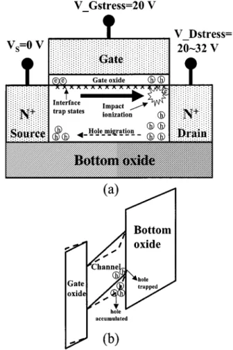
Fig. 4(a) shows the schematic diagram of the poly-Si TFTs degradation under static stress. The hot holes and electrons are generated from the impact ionization near the drain at high drain bias conditions. The injection efficiency into the gate oxide for hot holes and electrons depends on the vertical electric
field near the drain and
source [3]. At V and
Fig. 3. Variations of the threshold voltage shifts as a function of the stress time. The insert plots are the variations of the maximum transconductance as a function of the stress time.
Fig. 4. (a) Schematic diagram of the poly-Si TFTs degradation under the static stress and (b) the schematic energy band diagram for hot holes accumulated/trapped at the channel/bottom oxide interface.
V– V, the vertical field near drain is small for holes injection into the gate oxide. Thus, the increased in forward mode measurements are due to hot electrons trapped by the acceptor-like trap states at the gate oxide/channel
CHANG et al.: ANOMALOUS VARIATIONS OF OFF-STATE LEAKAGE CURRENT 257
interface and silicon grain boundaries (Fig. 1). On the other hand, the vertical field near source is high and favoring elec-trons injection into the gate oxide to increase in reverse mode measurements (Fig. 2). Therefore, in reverse mode measurements increases initially. Once the number of holes migrated from drain to source are larger than those of electrons trapped in the gate oxide, starts to decrease and the turnaround points in Fig. 2 can be observed. The path for holes migration is along the channel/bottom oxide interface because of the lowest potential for holes. The holes migrated from drain to source are accumulated and some are trapped at the
channel/bottom oxide interface [8]. At V and
V– V, the vertical electric field near drain is moderate and favoring holes injection into the gate oxide to lower in forward measurements. Under higher drain bias conditions, a greater number of holes will be generated by the impact ionization [9] and the lateral electric field along
channel is also enhanced. Therefore,
more number of holes with higher migration speed from drain to source will be accumulated/trapped at channel/bottom oxide interface near the source. Moreover, the time required for turnaround points are decreased as can be expected and seen in Fig. 2. Fig. 4(b) shows the schematic energy band diagram for the hot holes accumulated/trapped at the channel/bottom oxide interface. Because the electric field near the gate oxide/channel interface can be reduced, the induced by the high electric field can be also reduced.
IV. CONCLUSION
The anomalous variations in poly-Si TFTs under static stress are studied. Under low , the increased in forward mode measurements are due to hot electrons trapped by the acceptor-like trap states at the gate oxide/channel inter-face and silicon grain boundaries. Under high , the
lower in forward measurements can be attributed to the fact that the vertical electric field near drain is moderate and fa-voring holes injection into the gate oxide. Moreover, the holes accumulated/trapped at the channel/bottom oxide interface near the source are the dominating factors for lowering in re-verse mode measurements.
REFERENCES
[1] M. Hack, I.-W. Wu, T. J. King, and A. G. Lewis, “Analysis of leakage currents in poly-silicon thin film transistors,” in IEDM Tech. Dig., 1993, pp. 385–388.
[2] S. S. Bhattacharya, S. K. Banerjee, B. Y. Nguyen, and P. J. Tobin, “Temperature dependence of the anomalous leakage current in polysil-icon-on insulator MOSFETs,” IEEE Trans. Electron Devices, vol. 41, pp. 221–227, Feb. 1994.
[3] G. Fortunato, A. Pecora, G. Tallarida, L. Mariucci, C. Reita, and P. Migliorato, “Hot carrier effects in n-channel polycrystalline silicon thin-film transistors: A correlation between off-current and transcon-ductance variations,” IEEE Trans. Electron Devices, vol. 41, pp. 340–346, Feb. 1994.
[4] I.-W. Wu, W. B. Jackson, T. Y. Huang, A. G. Lewis, and A. Chiang, “Mechanism of device degradation in n- and p-channel polysilicon TFTs by electric stressing,” IEEE Electron Device Lett., vol. 11, pp. 167–169, Apr. 1990.
[5] V. Suntharalingan, S. J. Fonash, and O. O. Awadelkarim, “Device degra-dation in n- and p-channel polysilicon TFTs as a function of different electric stress configurations,” in AMLCD 1995 Dig., pp. 115–118. [6] F. V. Farmakis, J. Brini, G. Kamarinos, C. A. Dimitriadis, V. K.
Gue-orguiev, and Tz. E. Ivanov, “Leakage current variation during two dif-ferent modes of electric stressing in undoped hydrogenated n-channel polysilicon thin film transistors (TFTs),” Microelectron. Reliability, vol. 39, pp. 885–889, 1999.
[7] F. V. Farmakis, J. Brini, G. Kamarinos, and C. A. Dimitriadis, “Anoma-lous turn-on voltage degradation during hot-carrier stress in polycrys-talline silicon thin-film transistors,” IEEE Electron Device Lett., vol. 22, pp. 74–76, Feb. 2001.
[8] S. Inoue, H. Ohshima, and T. Shimoda, “Analysis of threshold voltage shift caused by bias stress in low temperature poly-Si TFTs,” in IEDM Tech. Dig., 1997, pp. 527–530.
[9] M. Koyanagi, H. Kurino, T. Hashimoto, H. Mori, K. Hata, Y. Hiruma, T. Fujimori, I.-W. Wu, and A. G. Lewis, “Relation between hot-carrier light emission and kink effect in poly-Si thin film transistors,” in IEDM Tech. Dig., 1991, pp. 571–574.