應用於無線近身網路之嵌入式晶體振盪器
71
0
0
全文
(2) 應用於無線近身網路之嵌入式晶體振盪器 An Embedded Crystal Oscillator for Wireless Body Area Network Applications 研 究 生: 黃上賓. Student: Shang-Bin Huang. 指導教授: 李鎮宜博士. Advisor: Dr. Chen-Yi Lee. 國立交通大學 電子工程學系電子研究所 碩士論文. A Thesis Submitted to Department of Electronics Engineering & Institute Electronics College of Electrical and Computer Engineering National Chiao Tung University in Partial Fulfillment of Requirements for the Degree of Master in Electronics Engineering August 2008 Hsinchu, Taiwan, Republic of China. 中華民國 九十七 年 八 月.
(3) 應用於無線近身網路之嵌入式晶體振盪器 研 究 生: 黃上賓 指導教授: 李鎮宜教授 國立交通大學電子工程學系電子研究所. 摘要 在本篇論文裡,我們介紹一個應用於無線近身網路的嵌入式晶體振盪器和基頻低功 率設計流程,來降低整個系統的功率消耗和面積使用。. 近年來,健康照護的系統應用於無線近身網路愈來愈受到人們的重視,尤其是針對 人體生醫訊號的偵測。在這樣的應用中,可以從配戴在身上的無線感測器對人體訊號做 長時間的偵測,並以無線的方式將資料傳送給整合在手機或個人數位助理的接收端。基 於這樣的一個應用,極低的功率消耗跟高度整合的面積會是系統不可或缺的需求。我們 使用了低功率的設計流程來降低整個基頻的功率消耗,儘管整個基頻的功率消耗已經非 常低。但從整個系統來看,我們可以發現功率消耗主要由晶片外部的一些元件佔非常大 的部份,像是石英晶體與其搭配使用的振盪器。不僅如此,這些晶片外部的元件同樣佔 據了相當大的面積使用,對整個系統造成額外的負擔,於是嵌入式晶體振盪器[1]被提出 來取代這些晶片外部所使用元件。嵌入式晶體振盪器是藉由互補金氧半導體製程的方 式,將晶體振盪器整合進單一晶片中,如此一來可以大大地降低系統的製造成本、面積 及功率消耗。在本篇論文我們對整個嵌入式晶體振盪器的行為做一個詳盡的闡述,並分 析頻率校準的設計,最後建立了一個嵌入式晶體振盪器的原型來驗證這樣的行為。藉由 使用嵌入式晶體振盪器以及基頻的低功率設計流程,整個系統將可以降低 73%的功率消 耗和 53%的面積使用。. -I-.
(4) An Embedded Crystal Oscillator for Wireless Body Area Network Applications Student: Shang-Bin Huang Advisor: Chen-Yi Lee Department of Electronics Engineering and Institute of Electronics, National Chiao-Tung University. Abstract In this thesis we propose an Embedded Crystal (eCrystal) oscillator and baseband low power design flow for Wireless Body Area Network (WBAN) applications to assure the overall system power and area reduction.. In the recent years, people have attached great importance to healthcare monitoring system for WBAN applications. There are multiple wireless sensor nodes (WSNs) placed on the human body for long-time monitoring. The WSNs transmit data wirelessly to a central processing node (CPN) integrated into mobile phones or personal digital assistants (PDAs). Ultra-low power and tiny integrated area are the features required in such applications. A low power design flow comprising Multiple Supply Voltage (MSV) and power gating is used to reduce baseband power consumption. However, the overall system power is dominated by some off-chip components, e.g. quartz crystal and oscillator. Besides, these external components also occupy very large system area. Therefore, an eCrystal oscillator [1] has been proposed to replace these external components, and this can largely reduce manufacturing cost, system area, and power consumption. We elaborate and analyze the frequency error calibration of eCrystal oscillator and establish the prototype platform to verify the system behavior with eCrystal oscillator. By the use of eCrystal oscillator and baseband low power design flow, the system will have 73% power reduction and 53% area reduction.. -II-.
(5) 誌謝 在 Si2 實驗室的碩士班研究過程中,讓我學到了非常多的東西。其中要感謝我的指 導教授李鎮宜博士,他提供了非常完善的研究環境與資源,使我們能夠從系統的各個層 面來發展及實現研究的方向。還有要感謝實驗室的鍾菁哲學長、游瑞元學長,在碩士班 裡給我的關心與指導,也要感謝實驗室的同學及學弟妹們:余建螢、陳燦文、陳俊廷、 郭冠麟、宋偉豪、馬曉涵,他們在我困惑時經常地提供意見與幫助。另外還要感謝我的 家庭給予的關心與鼓勵。在大家的支持下,我才能順利地完成碩士學業,最後感謝口試 委員的指導與寶貴的意見。. -III-.
(6) CONTENTS. CONTENTS. PAGE. Chapter 1 .................................................................................................................................... 1 Introduction ................................................................................................................................ 1 1-1 Motivation......................................................................................................................... 1 1-2 Organization...................................................................................................................... 5 Chapter 2 .................................................................................................................................... 6 Low Power Design Flow............................................................................................................ 6 2-1 Background ....................................................................................................................... 6 2-1-1 Multiple Supply Voltage ............................................................................................ 6 2-1-2 Power Gating ............................................................................................................. 7 2-2 Low Power Design Flow ................................................................................................ 10 2-3 Implementations.............................................................................................................. 11 2-3-1 Voltage/Power Domain Partitions............................................................................ 12 2-3-2 Power Gating Implementation................................................................................. 13 2-3-3 Power Gating and Isolation Timing Control............................................................ 13 2-4 Measurement Results ...................................................................................................... 16 Chapter 3 .................................................................................................................................. 20 Analysis of Embedded Crystal Oscillator ................................................................................ 20 3-1 System Overview ............................................................................................................ 20 3-2 System Behavior ............................................................................................................. 23 3-3 Frequency Detector......................................................................................................... 24 Chapter 4 .................................................................................................................................. 35 Emulation of Embedded Crystal Oscillator ............................................................................. 35 4-1 Building Block Design.................................................................................................... 36 4-1-1 Transmitter Node and Remote Reference................................................................ 36 4-1-2 Clock Generator....................................................................................................... 36 4-1-3 Frequency Detector.................................................................................................. 37 4-1-4 A/D and D/A Interface............................................................................................. 38 -IV-.
(7) CONTENTS 4-2 Case Studies .................................................................................................................... 39 4-2-1 Frequency Shift Keying Applications...................................................................... 39 4-2-2 Wireless Body Area Network Applications ............................................................. 43 Chapter 5 .................................................................................................................................. 50 Conclusions and Future Work .................................................................................................. 50 5-1 Conclusions..................................................................................................................... 50 5-2 Future Work .................................................................................................................... 50 References ................................................................................................................................ 52 Appendix .................................................................................................................................. 54 Supplementary of Power Gating Cell....................................................................................... 54. -V-.
(8) LIST OF FIGURES. LIST OF FIGURES. PAGE. Figure 1-1: Target operation scenario for WBAN applications ................................................. 2 Figure 1-2: The Quartz crystal used in a wireless electrocardiogram (ECG) patch (source: IMEC)......................................................................................................................................... 3 Figure 1-3: The power consumption of WSN ............................................................................ 4 Figure 1-4: The area of WSN ..................................................................................................... 5 Figure 2-1: Footer and Header fine-grain power gating implementation in NAND gate .......... 8 Figure 2-2: Header coarse-grain power gating implementations ............................................... 8 Figure 2-3: Ring style sleep transistor implementations............................................................ 9 Figure 2-4: Column style power gating implementations.......................................................... 9 Figure 2-5: The low power design flow for baseband chip implementation ........................... 10 Figure 2-6: The dual-mode baseband transceiver with (a) abstract view of functional blocks and (b) behavior time line ........................................................................................................ 11 Figure 2-7: The transceiver block diagram with power domain planning (a) wireless sensor node (WSN); (b) central processing node (CPN); (c) power management cell; (d) power management control sequence ................................................................................................. 12 Figure 2-8: The coarse-grain and column style power gating applied in this work................. 13 Figure 2-9: Current profile between sleep and active state ...................................................... 17 Figure 2-10: Micro chip photo (a) WSN; (b) CPN .................................................................. 18 Figure 2-11: The power consumption of WSN with low power design flow .......................... 19 Figure 3-1: The concept of eCrystal oscillator......................................................................... 20 Figure 3-2: The operation flow of eCrystal system.................................................................. 21 Figure 3-3: The accuracy of eCrystal oscillator for possible different applications ................ 22 Figure 3-4: Block diagram of the eCrsytal oscillator system................................................... 23 Figure 3-5: The FFT-based frequency detector ........................................................................ 25 Figure 3-6: The signal power of the best-case FFT detection.................................................. 26 Figure 3-7: The signal power of the worst-case FFT detection ............................................... 27 Figure 3-8: The calibration performance of different-size FFT ............................................... 28 Figure 3-9: The architecture of counter-based frequency detector .......................................... 29. -VI-.
(9) LIST OF FIGURES Figure 3-10: The counting error under different SNR conditions............................................ 32 Figure 4-1: Block diagram of the eCrystal emulation platform ............................................... 35 Figure 4-2: Block diagram of the DDFS.................................................................................. 36 Figure 4-3: The analog-to-digital bias circuit........................................................................... 38 Figure 4-4: The eCrystal oscillator prototype for FSK applications ........................................ 40 Figure 4-5: The initial case of eCrystal oscillator for FSK applications (a) Generated Clock; (b) Error Signal .............................................................................................................................. 41 Figure 4-6: The final results of eCrystal oscillator for FSK applications (a) Generated Clock; (b) Error Signal......................................................................................................................... 42 Figure 4-7: The eCrystal oscillator prototype for WBAN applications ................................... 44 Figure 4-8: The initial case of eCrystal oscillator for WBAN applications (a) Generated Clock; (b) Error Signal......................................................................................................................... 45 Figure 4-9: The final results of eCrystal oscillator for WBAN applications (a) Generated Clock; (b) Error Signal............................................................................................................. 46 Figure 4-10: The power consumption of WSN with low power design flow and eCrystal oscillator ................................................................................................................................... 48 Figure 4-11: The area of WSN with low power design flow and eCrystal oscillator .............. 49 Figure A-1: Power gating cell operation mechanism (a) PMOS header; (b) NMOS header ... 55 Figure A-2: NMOS: VD(0.5V)+ VG(0.9V) and PMOS VS(0.5V)+ VG(0V) (a) driving current; (b) transconductance ................................................................................................................ 59 Figure A-3: Testing circuit ....................................................................................................... 59 Figure A-4: VDDV pulled by PGC in the active state ............................................................. 60 Figure A-5: Leakage current in the sleep state......................................................................... 61. -VII-.
(10) LIST OF TABLES. LIST OF TABLES. PAGE. Table 1-1: The power consumption, area, and cost of the quartz crystal [2] ............................. 3 Table 2-1: Chip core power in WSN and CPN chipset ............................................................ 17 Table 2-2: Chip Summary ........................................................................................................ 18 Table 3-1: The specification of eCrystal oscillator .................................................................. 22 Table 3-2: The counting error requirement when different number of detection/calibration is applied ...................................................................................................................................... 32 Table 3-2: Comparisons of FFT-based and counter-based frequency detector ........................ 34 Table 4-1: The emulation results of eCrystal oscillator for WBAN applications .................... 47 Table 4-2: The power consumption and area of eCrystal oscillator [13] ................................. 48. -VIII-.
(11) Ch1. Introduction. Chapter 1 Introduction 1-1 Motivation With the increase of the world’s elderly population and modern work pressure, the population of various cardiovascular and other chronic diseases increases rapidly, and the age decreases year by year. In medical institutions, many sensors of physiological monitoring equipments were placed in patients and transmit signals to display devices by electric wires. Except testers feel uncomfortable by those wires, it is more dangerous to cause wires peeling when they shift beds or turn the bodies over. Besides, many physiological signals demand long-term and continuous monitoring. Therefore, the wireless transmission of physiological is more and more important for medical staff and patients.. In the Wireless Body Area Network (WBAN) applications, the goal of ubiquitous healthcare monitoring is to extend the physiological monitoring from the closed in-hospital environment to any open roaming spaces. The target operation scenario is illustrated in Figure 1-1, there are multiple wireless sensor nodes (WSNs) placed on the human body. Each WSN can perform physiological data sensing and processing, and transmit the data wirelessly to a central processing node (CPN) which may be integrated into a mobile phone or a personal digital assistant (PDA).. 1.
(12) Ch1. Introduction. Figure 1-1: Target operation scenario for WBAN applications. To achieve this ubiquitous healthcare monitoring in the WBAN applications, the system must provide highly reliable signal exchanges between the WSNs and CPN so that doctors will not make mistakes when estimating the patients’ condition. In addition to the reliability issue, the system, especially the WSN, is required to have ultra-low power (μW-level) with highly integrated tiny area. Smaller size not only reduces the manufacturing cost but also provide the convenience and portability. And the physiological signals usually need long-term and continuous monitoring to observe if there is something abnormal. Also, the working energy will be provided by the batteries with limited energy. Therefore, ultra-low power consumption is required for this system.. Figure 1-2 shows the quartz crystal used in a wireless electrocardiogram (ECG) patch. The quartz crystal plays an important role in the existing system to provide a reference clock, and usually needs extra passive components or a silicon oscillator pad to generate the reference clock frequency. This configuration has large overhead on power consumption (mW-level), area occupation, and manufacturing cost, as shown in Table 1-1 [2].. 2.
(13) Ch1. Introduction. Figure 1-2: The Quartz crystal used in a wireless electrocardiogram (ECG) patch (source: IMEC). Table 1-1: The power consumption, area, and cost of the quartz crystal [2] In-crystal. 1μW~200μW. Power consumption. 1mW~50mW (active) Oscillator 10μW~50μW (standby) SMD. 3.2mm x 2.5mm x 0.5mm. DIP. 11.5mm x 4.7mm x 3.5mm. Area. Cost. US$0.15~2. Figure 1-3 and Figure 1-4 show the power consumption and area of the WSN, exclusive the analog-to-digital converter (ADC). Except the baseband power consumption, the use of quartz crystal and oscillator occupy very large part of the WSN. Therefore, we apply low power design flow to achieve μW-level baseband power consumption. However, the off-chip components consume much more power and dominate the overall system power consumption. As a result, an Embedded Crystal (eCrystal) oscillator [1] has been proposed to replace these external 3.
(14) Ch1. Introduction components, which includes quartz crystal, oscillator, resistors, and capacitors, by a tunable process, voltage, and temperature (PVT) tolerance clock generator [3] with frequency error calibration. The clock generator is designed with limited initial frequency offset, say 3%, under any process, voltage, and temperature (PVT) variations, and the calibration loop provides a clock mismatch recovery to improve fine-tuning frequency error. With the eCrystal oscillator which can be integrated in standard CMOS process, the external components can be eliminated, and this results in large system area and manufacturing cost reduction. In this thesis the hardware design and system behavior of the eCrystal oscillator will be discussed and analyzed. And the prototype platform is established to verify the behavior of the eCrystal oscillator.. Figure 1-3: The power consumption of WSN. 4.
(15) Ch1. Introduction. Figure 1-4: The area of WSN. 1-2 Organization In this thesis, we use the baseband low power design design flow and eCrystal oscillator to reduce overall system power consumption and area usage. In the following chapters, the detailed design process and principle will be presented clearly.. In Chapter 2, the low power design flow applied for baseband chip implementation is presented.. In Chapter 3, the system behavior of eCrystal oscillator is described, and the architecture of frequency error calibration to improve fine-tuning frequency error is discussed and formulated.. In Chapter 4, the emulation design of building blocks in the eCrystal oscillator is discussed, and two prototypes for WBAN and FSK applications are demonstrated.. Finally, in Chapter 5, we summarize the conclusions and present the future work.. 5.
(16) Ch2. Low Power Design flow. Chapter 2 Low Power Design Flow In this chapter the low power techniques including Multiple Supply Voltage (MSV) and power gating will be introduced and applied to the low power design flow for baseband chip implementation.. 2-1 Background 2-1-1 Multiple Supply Voltage Multiple Supply Voltage (MSV), which is also called Voltage Island [4], is an effective power reduction technique, which operates different blocks at different voltages.. In previous generations, large functional blocks were not integrated in the single chip, so that the supply voltage of each block could be made independently. As advance of process technology, the chip capacity is increasing; therefore, more and more functional units will be integrated into the single chip, which is called System-on-Chip (SoC). These different functional blocks on the chip may have different performance requirements; hence MSV is used to lower down the voltage level of each block while maintaining the performance requirements.. To implement MSV on a system, the power domain partition should be defined in the front end, and created during the floor-planning stage of physical design for the following placement and optimization. In the MSV implementation, every signal that. 6.
(17) Ch2. Low Power Design flow. crosses different power domains requires a level shifter to convert one voltage level to another. Although level shifting from a higher-voltage power domain to a lower one is usually optional, level shifting from a lower-voltage power domain to a higher one is necessary. Besides, the size of level shifter should be chosen carefully to ensure the signal integrity when crossing different power domains.. 2-1-2 Power Gating Power gating comes from Multi-threshold CMOS (MTCMOS) technique [5-6], which is very effective for reducing leakage current in the sleep state. The concept of MTCMOS is to use both high-VT and low-VT devices on a chip. High-VT devices can be used for leakage current reduction while low-VT devices can be used for higher performance requirement. Furthermore, MTCMOS involves using high-VT transistors to gate power supplies of a low-VT logic circuit. When the high-VT transistors are turned on, the low-VT logic block is connected to power supplies and goes to active state. When the low-VT logic circuit enters the sleep state, the high-VT transistors are turned off for leakage current reduction.. From another point of view, using MTCMOS technique in every standard cell is also called fine-grain or cell-based power gating implementation [7], as shown in Figure 2-1. The advantage of the fine-grain power gating implementation is that the virtual power rails are short and hidden in the cell. However, the power switches which are added in every standard cell result in significant area overhead. Moreover, the normal standard cells provided by library vendors and ASIC foundries can not be used. What’s more important issue is that the built-in power switch is subject to PVT variation, which results in added IR-drop variation, or performance variation, in the cell. 7.
(18) Ch2. Low Power Design flow. Figure 2-1: Footer and Header fine-grain power gating implementation in NAND gate. On the other hand, in the coarse-grain or distributed power gating implementation [7], which is shown in Figure 2-2, the power switches are connected between the real power rail and the virtual power rail networks. The main advantage of the coarse-grain power gating implementation is that all power switches can share charge/discharge current. Consequently, it is less sensitive to PVT variation and also less IR-drop variation compared with the fine-grain power gating implementation. Moreover, the area overhead is significantly smaller due to the charge sharing among the power switches.. Figure 2-2: Header coarse-grain power gating implementations. 8.
(19) Ch2. Low Power Design flow. In addition to fine/coarse-grain power gating, the ring/column style is also an important issue for power gating implementation. The ring style power network shown in Figure 2-3 has less complexity on Auto Place and Route (APR) flow but worse IR-drop performance because the real power line is far from the center of the power domain.. Figure 2-3: Ring style sleep transistor implementations. On the other hand, the column style power network shown in Figure 2-4 has better IR-drop performance but is more complex on APR flow.. Figure 2-4: Column style power gating implementations. 9.
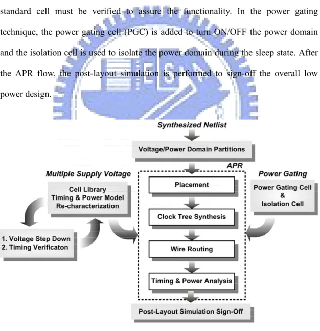
(20) Ch2. Low Power Design flow. 2-2 Low Power Design Flow Based on the typical cell-based design flow, the low power techniques including MSV and power gating are added to achieve low power design, as shown in Figure 2-5. Before the APR, the voltage/power domain partitions must be defined first to apply MSV and power gating. To apply voltage-scaling approach in MSV technique, the timing and power models of cell libraries provided from the foundries should be re-characterized. And every time the supply voltage is stepped-down, the timing of standard cell must be verified to assure the functionality. In the power gating technique, the power gating cell (PGC) is added to turn ON/OFF the power domain and the isolation cell is used to isolate the power domain during the sleep state. After the APR flow, the post-layout simulation is performed to sign-off the overall low power design.. Figure 2-5: The low power design flow for baseband chip implementation. 10.
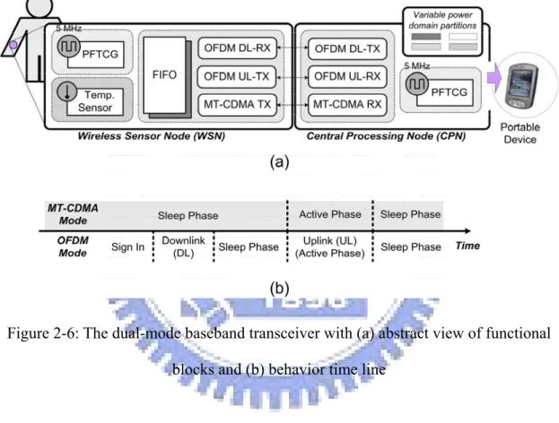
(21) Ch2. Low Power Design flow. 2-3 Implementations The 0.5V 7Mbps baseband transceiver chipset, consists of WSN and CPN, is designed for WBAN applications. The system block diagram and behavior time-line are illustrated in Figure 2-6. The baseband processor provides both MT-CDMA and OFDM modes for different data rate requirements.. Figure 2-6: The dual-mode baseband transceiver with (a) abstract view of functional blocks and (b) behavior time line. The low power design flow, including MSV and power gating, is applied for this baseband chip implementation to reduce both dynamic and static power consumptions, as illustrated in Figure 2-7.. 11.
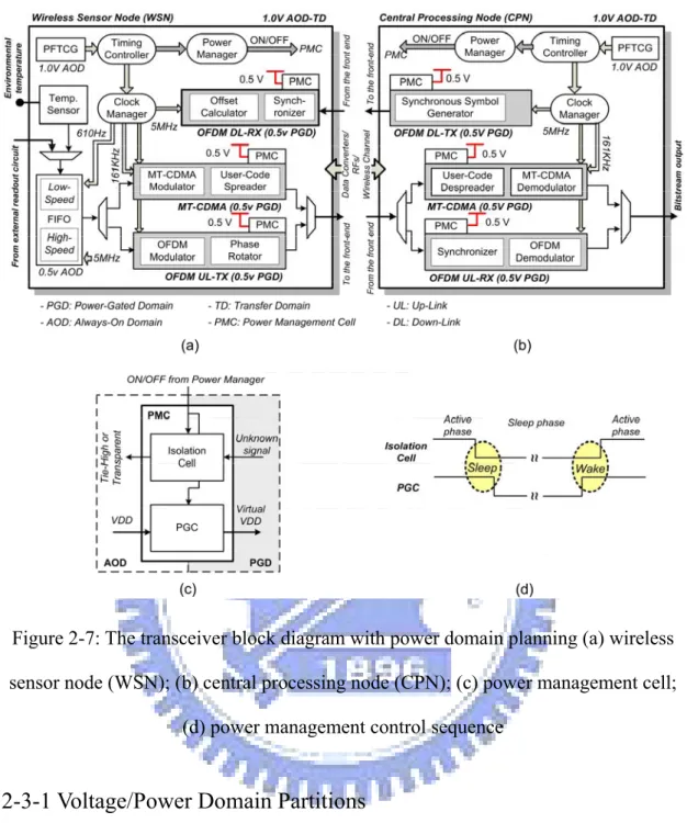
(22) Ch2. Low Power Design flow. Figure 2-7: The transceiver block diagram with power domain planning (a) wireless sensor node (WSN); (b) central processing node (CPN); (c) power management cell; (d) power management control sequence. 2-3-1 Voltage/Power Domain Partitions This system is partitioned into 12 power domains, which are designed with different supply voltages to reduce total power consumption. In this baseband transceiver chipset, the main functional blocks are operated at 0.5V according to the required performance and achievable functionality. Except for the main functional blocks, there are several special functional blocks, Phase and Frequency Tunable Clock Generator (PFTCG) and Temperature Sensor (TS), which are designed at 1.0V. Moreover, a transfer-domain (TD) including the control units is defined and operated 12.
(23) Ch2. Low Power Design flow. at 1.0V to be an interface between the functional blocks and I/O pads.. 2-3-2 Power Gating Implementation Considering the large area overhead and higher PVT sensitivity of fine-grain power gating and larger IR-drop of ring style power gating, the coarse-grain and column style power gating implementation is applied in this work, as shown in Figure 2-8.. Figure 2-8: The coarse-grain and column style power gating applied in this work. Moreover, there are different characteristics for different types of power switches. For example, PMOS transistor is less leaky than NMOS transistor of a same size, while NMOS transistor has higher drive current than PMOS transistor of a same size and hence small area overhead [7]. And this comparison will be discussed in the Appendix.. 2-3-3 Power Gating and Isolation Timing Control In the baseband chipset shown in Figure 2-6, the main functional blocks will not work at the same time according to different operation modes. Therefore, the 13.
(24) Ch2. Low Power Design flow. non-active power domains can be switched into sleep state for leakage current reduction. The behavior of power-on/off control can be achieved by the aid of power management cell (PMC), which contains coarse-grain and column style power gating cells (PGCs) and isolation cells shown in Figure 2-7(c).. The power-gated domain (PGD) can be turned ON/OFF by the control sequences from the power manager in the TD, and Figure 2-7(d) shows the waveform of control sequences, which includes power gating and isolation. When the PGD is going to sleep state, an OFF signal asserted from the power manager will make isolation cell isolate the signal from the PGD, and the signal to the always-on domain (AOD) will be tied high. After that, the PGCs shut off the virtual power supply of PGD. By the use of above two control sequences, the PGD can be switched into sleep state, and the operations of logic blocks in the AOD will not be affected by the unknown signal from the power-off PGD. When the PGD is going to active state, the PMC will act in the reverse order of above two control sequences, i.e. the PGCs will turn on the PGD first, and the signal from PGD can pass through the disabled isolation cell to the AOD. Besides, the special functional blocks need to work continually; therefore, the corresponding power domains will not be gated and is regarded as AOD.. In the WSN design shown in Figure 2-7(a), there are 3 main functional blocks to support the dual-mode transmission and pre-calibration [8], i.e. MT-CDMA transmitter (TX), OFDM down-link (DL) receiver (RX), and OFDM up-link (UL) transmitter (TX). According to different operation modes, these 3 functional blocks will not work at the same time. Consequently, they are partitioned as 3 different PGDs, including 0.5V OFDM DL-RX, 0.5V MT-CDMA TX, and 0.5V OFDM UL-TX. In addition to the 3 main functional blocks, the other functional blocks are partitioned as. 14.
(25) Ch2. Low Power Design flow. AODs, which include 0.5V FIFO, 0.8V PFTCG, 1.0V TS, and the other control units in the 1.0V TD.. The 3 main functional blocks and corresponding PGDs will act as the following mechanism. First of all, in the MT-CDMA TX mode, the FIFO stores the sensed body signals whereas the MT-CDMA transmitter is powered off in the sleep state. When the data storage is complete, the MT-CDMA transmitter will be waked up and enters active state to transmit those signals. Secondly, in the OFDM DL-RX mode, the OFDM receiver is going to active state and performs synchronization and pre-calibration. Lastly, the OFDM UL-TX mode is similar to the MT-CDMA TX mode, the OFDM transmitter is turned off in the sleep state when waiting for data storage and is turned on to transmit data when the data storage is complete. In these 3 operation modes, only the corresponding PGD will be powered on, the other two PGDs are turned off to suppress the leakage current.. In the CPN design shown in Figure 2-7(b), there are also 3 main functional blocks to perform dual-mode modulation, i.e. MT-CDMA RX, OFDM DL-TX, and OFDM UL-RX. Similar to the WSN, these 3 main functional blocks will not work together with different operation modes. Accordingly, they are partitioned into 3 different PGDs, including 0.5V MT-CDMA RX, 0.5V OFDM DL-TX, and 0.5V OFDM UL-RX. Additionally, the other functional blocks which always stay active are partitioned as the AODs, including 0.8V PFTCG and the other control in the 1.0V TD.. The 3 main functional blocks and corresponding PGDs will operate as the following mechanism. First, in the MT-CDMA RX mode, the data received from the front-end is directed to the MT-CDMA receiver, and the MT-CDMA receiver will be turned on to perform user-code de-spread and demodulation. Secondly, in OFDM 15.
(26) Ch2. Low Power Design flow. DL-TX mode, the OFDM transmitter is waked up to broadcast the synchronous symbols. Finally, in the OFDM UL-RX mode, the received data is switched to the OFDM receiver, and the OFDM receiver will enter into active state and perform the synchronization first followed by the demodulation. In these 3 operation modes, only the corresponding PGD is activated and the other two PGDs are switched into the sleep state.. 2-4 Measurement Results The baseband transceiver chipset is fabricated in 90nm 1P9M CMOS standard process, which provides the devices of high- and regular-threshold voltages (SPHVT and SPRVT). Both devices are applied in this design where the high-threshold voltage device is used in the non-critical path for leakage power reduction, and the regular-threshold one is used in the critical path to maintain required performance. The measurement instruments include a constant-temperature oven, LeCroy LC584A, and a current-meter with resolution of 100pA.. The building blocks in this chip are designed with individual groups of power pads to measure the power consumption of each building block separately. Table 2-1 shows the measured core power consumption of power domain in the corresponding operation mode.. 16.
(27) Ch2. Low Power Design flow. Table 2-1: Chip core power in WSN and CPN chipset WSN. CPN DL-TX. 3.94 μW. UL-RX. 520 μW. MT-RX. 490 μW. Total 5.52 μW Modulator. FIFO+TS. 289.5 μW. N/A. N/A. PFTCG. 145.8 μW. PFTCG. 145.8 μW. The PGDs in this chip are turned ON/OFF by the PGCs for different operation modes. The OFDM DL-TX mode is used for the illustration of the current profile between active and sleep states. To observe the current variation, a resistor (51K ohm) is concatenated in the path between the power supply and the chip. Therefore, the cross voltage between the resistor’s two sides can be measured and is shown in Figure 2-9. When the ENABLE signal is activated, the OFDM DL-TX PGD will be turned on and goes to active state, and the current can be derived by the measured voltage and the concatenated resistor (current = (measured volatage)/51Kohm).. Figure 2-9: Current profile between sleep and active state 17.
(28) Ch2. Low Power Design flow. In this baseband transceiver chipset, the transmission power is reduced from previous proposal 21μW [9] to this work 5.52μW, and this results in 73.7% efficiency improvement in baseband circuit processing. Figure 2-10 shows the micro chip photos, where each bold-rectangular denotes an individual power domain, and the rest regions between separate power domains represents the TD for I/O-pad interfaces. Table 2-2 shows the short summary of this baseband transceiver chipset.. Figure 2-10: Micro chip photo (a) WSN; (b) CPN. Table 2-2: Chip Summary Standard 90nm Technology SPHVT/SPRVT CMOS Core Supply Voltage. 1.0V/0.5V 4.85Mbps (OFDM). Max. Data Rate 143kbps (MT-CDMA) WSN: 2191μm × 3030μm Die Size CPN: 1980μm × 2980μm. 18.
(29) Ch2. Low Power Design flow. With the baseband low power design flow, the power consumption of WSN is shown in Figure 2-11. The baseband power consumption has 63% reduction; however, WSN has only 6.4% power reduction when taking external quartz crystal and oscillator into account. Accordingly, eCrystal oscillator is used to replace the external quartz crystal and oscillator to further reduce overall system power consumption and area.. Figure 2-11: The power consumption of WSN with low power design flow. 19.
(30) Ch3. Analysis of Embedded Crystal Oscillator. Chapter 3 Analysis of Embedded Crystal Oscillator In this chapter, the behavior of eCrystal oscillator will be described. The eCrystal oscillator has a tunable clock generator with limited initial frequency offset, say 3%, under any PVT variations, and a frequency detector to estimate and calibrate the frequency error. The frequency detector is a very important building block to perform frequency error calibration; therefore the low-cost counter-based frequency detector is proposed to implement this frequency detector.. 3-1 System Overview. Figure 3-1: The concept of eCrystal oscillator 20.
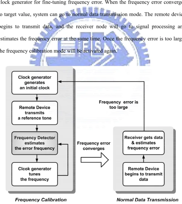
(31) Ch3. Analysis of Embedded Crystal Oscillator. Figure 3-1 shows the concept of eCrystal oscillator to replace the external components. A remote reference tone is used to calibrate the initial frequency offset of clock generator. By the use of eCrystal oscillator, the external components can be eliminated and integrated into single functional chip. Figure 3-2 shows the operation flow of eCrystal system. First the clock generator generates an initial clock with certain frequency offset, and then a reference tone will be transmitted from remote device. Second, the frequency detector estimates the error frequency and feedback to clock generator for fine-tuning frequency error. When the frequency error converges to target value, system can go to normal data transmission mode. The remote device begins to transmit data, and the receiver node will go to signal processing and estimates the frequency error at the same time. Once the frequency error is too large, the frequency calibration mode will be activated again.. Figure 3-2: The operation flow of eCrystal system. 21.
(32) Ch3. Analysis of Embedded Crystal Oscillator. Figure 3-3 shows the accuracy of eCrystal system for possible different applications. The un-calibrated clock generator is only for low-accuracy applications, e.g. micro-control unit (MCU). For WBAN applications, the eCrystal oscillator should provide the frequency error less than 50ppm by the use of calibration loop.. Figure 3-3: The accuracy of eCrystal oscillator for possible different applications. Table 3-1 summarizes the specification of eCrystal oscillator for WBAN applications. The maximum initial frequency offset of clock generator is 3%, and the fine-tuning resolution and detection resolution of frequency error calibration is 50ppm. Besides, the WSN for WBAN applications is designed to have a 512x8b FIFO storing body signals before transmission. Therefore, the allowable calibration time can derived from FIFO_Size/Sensor_Clock = 512/610 = 840ms.. Table 3-1: The specification of eCrystal oscillator Clock. Initial Frequency Offset. 3%. Generator. Fine-Tuning Resolution. 50ppm. Calibration. Detection Resolution. 50ppm. Loop. Calibration Time. 840ms. 22.
(33) Ch3. Analysis of Embedded Crystal Oscillator. 3-2 System Behavior. Figure 3-4: Block diagram of the eCrsytal oscillator system. Figure 3-4 shows the system block diagram of the eCrystal oscillator integrated into the receiver node. The quartz crystal in the receiver node is replaced by eCrystal oscillator. To reduce the initial frequency offset of clock generator, a frequency detector is used to estimate and calibrate the frequency error. First, the remote reference with channel noise can be written as Equation 3-1.. c ( t ) = cos 2π ( N syn ⋅ f o ) t + η. (3-1). where fo is baseband frequency, Nsyn is the magnification of synthesizer, and η represents the channel noise. Then the channel noise outside the required bandwidth is filtered by the Band Pass Filter (BPF). And the signal after BPF can be written as Equation 3-2. x ( t ) = cos 2π ( N syn ⋅ f o ) t. 23. (3-2).
(34) Ch3. Analysis of Embedded Crystal Oscillator. Secondly, the output frequency of clock Generator can be written as fo(1+ε) where ε is the normalized frequency error. And the mixer down-converts this remote reference to the baseband. The output of mixer can be derived as Equation 3-3. m ( t ) = cos 2π ( N syn ⋅ f o ) t × cos 2π ⎡⎣ N syn ⋅ f o ⋅ (1 + ε ) ⎤⎦ t =. 1 1 cos 2π ( N syn ⋅ f o ⋅ ε ) t + cos 2π ⎡⎣ N syn ⋅ f o ⋅ ( 2 + ε ) ⎤⎦ t 2 2. (3-3). The Low Pass Filter (LPF) is used to filter out the latter high-frequency term in Equation 3-3. Therefore the output of LPF remains the former low-frequency term in Equation 3-4. 1 1 y ( t ) = cos 2π ( N syn ⋅ f o ⋅ ε ) t = cos 2π ( f d ) t 2 2. (3-4). where fd represents the frequency of y(t). Lastly, the frequency detector is used to detect the frequency component of y(t), and the normalized frequency error, ε, can be derived as Equation 3-5.. ε=. fd N syn ⋅ f o. (3-5). After the frequency detection, the frequency error can be fed back to the clock generator for fine-tuning frequency error, and hence the clock mismatch can be recovered. Finally, the baseband circuit will use the output clock of eCrystal oscillator to perform signal processing.. 3-3 Frequency Detector To reduce the initial frequency offset of clock generator, the frequency detector is an important building block to perform frequency error calibration. When the 24.
(35) Ch3. Analysis of Embedded Crystal Oscillator. frequency components of the error signal are detected, the frequency error can be derived for clock generator fine-tuning frequency error.. A Fast Fourier Transform (FFT)-based frequency detector shown in Figure 3-5 can analyze the frequency components of error signal. To use FFT-based frequency detector, an analog-to-digital converter (ADC) is needed to convert the error signal from analog to digital for frequency detection. After the error signal is sampled by the ADC, the frequency is detected by the FFT; therefore the clock generator can adjust its output frequency according to the estimated frequency error.. Figure 3-5: The FFT-based frequency detector. The main advantage of FFT-based approach is that the error signal is analyzed in the frequency domain, which means the signal will not be sensitive to the noise. This can be derived via simple signal power analysis. Assume that the error signal is sampled by 4x over-sampling ADC, i.e. the sampling clock rate is 4fo(1+ε), denoted as fsample. When an N-point FFT is applied, the resolution of FFT is fsample/N. If the frequency of error signal, fd, is integer multiples of the resolution of FFT, i.e.. fd = k ⋅. f sample N. , k=0,1,...,N-1. (3-6). This can be viewed as the best case of FFT frequency detection, which means the 25.
(36) Ch3. Analysis of Embedded Crystal Oscillator. frequency components will have only one signal tone in the frequency domain. Define the signal power as Equation 3-7. N −1. Ps = ∑ y [ n ] = 2. n =0. N 4. (3-7). The peak power term is N/4, as shown in Figure 3-6. The noise margin (NM) will have about 300dB, which is a very large value.. Figure 3-6: The signal power of the best-case FFT detection. When the detected frequency is not integer multiples of the resolution of FFT, it can be written as Equation 3-8.. fd ≠ k ⋅. f sample N. , k=0,1,...,N-1. (3-8). And the frequency components will appear a sinc distribution in the frequency domain. Therefore, the peak power term is about N/8. The worst case will occur when the detected frequency locates in the middle of two integer multiples, i.e. 26.
(37) Ch3. Analysis of Embedded Crystal Oscillator. 1 ⎞ f sample ⎛ , k=0,1,...,N-1 fd = ⎜ k + ⎟ ⋅ 2⎠ N ⎝. (3-9). In the worst case, the NM will be about 9.3dB, as shown in Figure 3-7.. Figure 3-7: The signal power of the worst-case FFT detection. Assume the signal-to-noise ratio (SNR) is s dB, and the signal power is N/2, the total noise power can be derived as Equation 3-10.. 10log10. Ps P N = s ⇒ Pw = ss = s Pw 1010 2 ⋅1010. (3-10). The total noise power will be uniform-distributed in each sub-carrier. So the noise power in each sub-carrier will be 1/(2.10s/10). Therefore, the tolerable SNR according to the worst-case detection can be derived as Equation 3-11.. 1 s 10. 2 ⋅10. <. NM ⇒ s > −9.6dB 2. 27. (3-11).
(38) Ch3. Analysis of Embedded Crystal Oscillator. The SNR requirement of FFT-based approach is much smaller, which means the FFT-based approach is nearly noise-free. However, the SNR requirement of proposed OFDM-based baseband signal processing for WBAN applications is about 3~4dB. And this implies FFT-based approach will over-design too much. Since the FFT-based approach is noise-free, the accuracy of FFT-based frequency detection only depends on the resolution of the space of FFT sub-carriers, i.e. fsample/N. Figure 3-8 shows the remaining frequency error when different-point FFT with 4x over-sampling ADC is used. It is found that the final frequency error can be converged to less than 50ppm when at least 4096-point FFT is applied.. Figure 3-8: The calibration performance of different-size FFT. Although the FFT-based frequency detection has strong interference rejection capability, the large-size FFT and extra ADC circuit are needed for required performance. Consequently, the larger hardware cost will be the disadvantage of FFT-based frequency detection. 28.
(39) Ch3. Analysis of Embedded Crystal Oscillator. From another point of view, the error signal can be analyzed in the time domain. A counter-based frequency detector can be used for this time-domain frequency detection, as shown in Figure 3-9.. Figure 3-9: The architecture of counter-based frequency detector. First, the number of cycles for the clock generator is chosen to be a referenced detection time. In this detection time, the number of cycles for the error signal will be derived according to different frequency errors. This relationship can be written as. ⎛ 1 ⎞ ⎛ 1 ⎜ ⎟ × N clk = ⎜ ⎝ f clk ⎠ ⎝ f err. ⎞ ⎟ × N err ⎠. (3-12). where fclk and ferr are the frequency of clock generator and error signal, Nclk and Nerr are the counted number of cycles for the frequency of clock generator and error signal, respectively. On the other hand, the frequency of clock generator and error signal can 29.
(40) Ch3. Analysis of Embedded Crystal Oscillator. be represented in terms of the frequency error between the frequency of clock generator and desired frequency. ⎧⎪ f clk = f o (1 + ε ) ⎨ ⎪⎩ f err = N syn ⋅ f oε. (3-13). We may combine Equation 3-12 and Equation 3-13 to find the ratio of Nclk and Nerr. N clk 1+ ε 1 = ≈ N err N syn ⋅ ε N syn ⋅ ε. (3-14). Therefore ε can be derived in terms of Nerr, Nclk, and Nsyn.. ε=. N err N err ≈ N syn ⋅ N clk − N err N syn ⋅ N clk. (3-15). If Nclk for fclk is chosen as fixed value, the frequency error, ε, can be derived according to detected Nerr for ferr. Assume the estimation of Nerr has counting error, i.e.. Nˆ err = N err (1 + CE ). (3-16). where Nˆ err is the estimation of Nerr and CE is the counting error. And the estimation of frequency error can be written as Equation 3-17.. εˆ ≈. N (1 + CE ) Nˆ err = err = ε (1 + CE ) N syn ⋅ N clk N syn ⋅ N clk. (3-17). where εˆ is the estimation of ε. Let the frequency error before calibration is εbefore and the frequency error after calibration is εafter. To perform detection and calibration successfully, the difference between real and estimated frequency error before 30.
(41) Ch3. Analysis of Embedded Crystal Oscillator. calibration should be less than target frequency error after calibration, i.e.. ε before − εˆbefore ≤ ε after. (3-18). Substitute Equation 3-17 into Equation 3-18 then we can derive the requirement of CE.. CE ≤. ε after ε before. (3-19). For one-shot detection/calibration, εbefore is the initial frequency offset (3%) and εafter is the target frequency error (50ppm). Therefore the counting error, CE, must be less than 0.17%. If K times detection/calibration is performed, CE to the power of K must be less than the ratio of initial frequency offset and target frequency error.. ( CE ) Table. 3-2. lists. the. CE. K. ≤. ε init = 0.17% ε tar. requirement. when. (3-20). different. number. of. detection/calibration is applied. The SNR requirement of proposed OFDM-based baseband signal processing is about 3~4dB. Figure 3-10 shows the CE under different SNR conditions. It is found that the number of detection/calibration must be larger than 3 times.. 31.
(42) Ch3. Analysis of Embedded Crystal Oscillator. Table 3-2: The counting error requirement when different number of detection/calibration is applied Number of Detection/Calibration. Counting Error Requirement. 1. 0.17%. 2. 4.08%. 3. 11.86%. 4. 20.21%. Figure 3-10: The counting error under different SNR conditions. Besides, the minimum value of Nclk is required so that Nerr can occur at least once. Therefore, the each minimum clock cycle of detection can be written as Equation 3-21.. 32.
(43) Ch3. Analysis of Embedded Crystal Oscillator. N clk ,min =. 1 + ε after N syn ⋅ ε after. (3-21). And total clock cycles of K times detection can be summed and written as Equation 3-22.. K. 1 + ε after ,k. ∑N k =1. syn. ⋅ ε after ,k. , k=1,2," ,K. (3-22). Table 3-2 summarizes the comparisons of these two frequency detectors. The FFT-based frequency detector has very good noise rejection capacity due to frequency-domain detection. However, the required high hardware cost implies it over-design too much. On the other hand, the counter-based frequency detector can meet the performance when several times detection/calibration is applied. And the most important is that counter-based approach has low complexity and low cost. Therefore, it is suitable for the implementation of frequency detector.. 33.
(44) Ch3. Analysis of Embedded Crystal Oscillator. Table 3-2: Comparisons of FFT-based and counter-based frequency detector Counter-based approach. FFT-based approach. Signal Domain. Time. Frequency. SNR Requirement (dB). > 8 (K=1). @Number of. 5.2 (K=2) -9.6 (K=1). Detection/Calibration. 3.8 (K=3). (K). 3.2 (K=4) K. Detection Time. 1 + ε after ,k. ∑N k =1. syn. ⋅ ε after ,k. , k=1,2," ,K. (clock cycle). N + log 2 N + N (8k@N=4096). (100x@K=3) 144k [10] Area Cost. 0.46k (N=4096, exclusive. (gate count). (K=3) ADC). 34.
(45) Ch4. Emulation of Embedded Crystal Oscillator. Chapter 4 Emulation of Embedded Crystal Oscillator In this chapter we design and implement the hardware emulation of eCrystal oscillator for Frequency Shift Keying (FSK) and WBAN applications, as shown in Figure 4-1. First we discuss the design considerations and hardware implementations of each building block in the emulation platform, especially clock generator and frequency detector. And then we show the testing results of the frequency error calibration.. Figure 4-1: Block diagram of the eCrystal emulation platform. 35.
(46) Ch4. Emulation of Embedded Crystal Oscillator. 4-1 Building Block Design 4-1-1 Transmitter Node and Remote Reference Compared with the block diagram of proposed eCrystal system shown in Figure 3-4, the remote reference and BPF are emulated by a synthesizer with reference frequency generated from the function generator.. 4-1-2 Clock Generator A direct digital frequency synthesizer (DDFS)-based clock generator can be used to emulate the clock generator. Figure 4-2 shows a typical architecture of DDFS [5], which can synthesis different frequencies corresponding to different digital control words.. Figure 4-2: Block diagram of the DDFS. The DDFS uses a phase accumulator which is supplied by a frequency digital control word. This accumulator addresses a Read Only Memory (ROM) that contains amplitude values of desired wave shape. And the ROM supplies commands to the digital-to-analog converter (DAC) for conversion to quantized analog signals. When the ROM is large enough, the DDFS can describe the desired wave with more amplitude values, i.e. the generated frequency will be close to the desired frequency.. 36.
(47) Ch4. Emulation of Embedded Crystal Oscillator. As a result, DDFS is capable to achieve much higher resolution. However, it still needs an external quartz crystal to achieve accurate frequency synthesis. In other word, it can not be the real clock generator since the external quartz crystal is needed. Even so, the DDFS still can be a good emulation for clock generator in eCrystal oscillator due to its quite good ability on higher resolution.. In the emulation platform, a programmable DDFS chip with controller is used to implement the clock generator. The input reference clock can be multiplied by 4~31 integer multipliers and the multiplied reference clock can be synthesized according to different frequency tuning words (FTW). The desired clock can be derived as Equation 4-1.. FTW =. desired clock × 248 ref . clock × multiplier. (4-1). where FTW is a 48-bit programmable tuning word. By the use of tunable DDFS-based clock generator, the initial frequency offset and fine-tuning ability can be emulated.. 4-1-3 Frequency Detector The proposed counter-based frequency detector has lower design complexity since only simple counters are used. The principle of counter-based frequency detection has been introduced in Section 3-3. Although the frequency error, ε, can be derived from Equation 3-15 theoretically, it needs to be mapped to the frequency tuning steps of the clock generator. And this effort will increase the design complexity of counter-based frequency detector. Furthermore, when two frequency errors which have the same amount but opposite signs, i.e. ε1 = -ε2, are detected, the frequency detector can not differentiate the generated frequency is higher or lower than the. 37.
(48) Ch4. Emulation of Embedded Crystal Oscillator. desired frequency from the counting results. Therefore, the frequency detector just guesses a direction and ask clock generator to move some testing tuning steps in the first frequency detection. After the generated frequency is changed and detected again, the frequency detector will compare new detection results with old one and keep the same direction for the decision, until the new frequency error is larger than old one in the following frequency detection.. 4-1-4 A/D and D/A Interface The synthesizers and down-mixer are operated in analog domain, while the eCrystal oscillator is operated in the digital domain. Therefore, a digital-to-analog interface is needed before the output frequency of clock generator is synthesized. This can be realized by simple dc-blocking capacitor. On the other hand, an analog-to-digital interface is needed before the error signal is detected by the frequency detector. This can be achieved by a resistor-and-capacitor bias circuit as shown in Figure 4-3. The capacitor C can block possible dc-offset of the output of demodulator and the ratio of resistors R1 and R2 can adjust output bias voltage. It is important to select the values of resistor and capacitor carefully to prevent from affecting the signal bandwidth. Moreover, a variable-gain amplifier (VGA) can be added to enlarge the amplitude of down-conversion frequency error.. Figure 4-3: The analog-to-digital bias circuit. 38.
(49) Ch4. Emulation of Embedded Crystal Oscillator. 4-2 Case Studies 4-2-1 Frequency Shift Keying Applications A hardware prototype to emulate the eCrystal oscillator integrated into receiver node for FSK applications is shown in Figure 4-4. The frequency band is 434MHz which belongs to industrial, scientific and medical (ISM) band. A well-developed FSK transceiver is used for the system platform, and baseband system clock is designed at 14.72MHz, i.e. the target generated clock is 14.72MHz.. The synthesizers and down-mixer are selected according to the required bandwidth. And the building blocks of eCrystal oscillator, clock generator and frequency detector, are implemented by Field Programmable Gate Array (FPGA). Figure 4-5(a) shows the testing case when the clock generator has 1% initial frequency offset, i.e. the generated clock is about 14.57MHz. The corresponding error signal is around 4MHz, as shown in Figure 4-5(b). After frequency error is detected and calibrated, the error signal is converged to 68ppm, which corresponds to 21.7kHz as shown in Figure 4-6(b). Figure 4-6(a) shows that the generated clock is tuned to 14.721MHz and provides system clock for baseband processing.. 39.
(50) Ch4. Emulation of Embedded Crystal Oscillator. Figure 4-4: The eCrystal oscillator prototype for FSK applications. 40.
(51) Ch4. Emulation of Embedded Crystal Oscillator. Figure 4-5: The initial case of eCrystal oscillator for FSK applications (a) Generated Clock; (b) Error Signal. 41.
(52) Ch4. Emulation of Embedded Crystal Oscillator. Figure 4-6: The final results of eCrystal oscillator for FSK applications (a) Generated Clock; (b) Error Signal. 42.
(53) Ch4. Emulation of Embedded Crystal Oscillator. 4-2-2 Wireless Body Area Network Applications A hardware prototype to emulate the eCrystal oscillator integrated into the WSN of Wireless Body Connection (WiBoC) baseband transceiver for WBAN applications, as shown in Figure 4-7. The frequency band is 1.4GHz which belongs to a set of wireless. medical. telemetry. service. (WMTS). band. defined. by. Federal. Communications Commission (FCC) [12]. And the baseband system clock is designed at 5MHz, i.e. the target generated clock is 5MHz.. The synthesizers and down-mixer are selected according to the required bandwidth. And the building blocks of eCrystal oscillator, clock generator and frequency detector, are implemented by FPGA. Figure 4-8(a) shows the testing case when the clock generator has initial frequency offset equal to 1500ppm, i.e. the generated clock is about 4.993MHz. The corresponding error signal for frequency detection is around 1.96MHz, as shown in Figure 4-8(b). After the frequency error is detected and calibrated, the fine-tuning frequency error is converged to 40ppm, which corresponds to about 59.1kHz as shown in Figure 4-9(b). Figure 4-9(a) shows that the generated clock is tuned to 4.9998MHz and provides system clock for baseband processing.. 43.
(54) Ch4. Emulation of Embedded Crystal Oscillator. Figure 4-7: The eCrystal oscillator prototype for WBAN applications. 44.
(55) Ch4. Emulation of Embedded Crystal Oscillator. Figure 4-8: The initial case of eCrystal oscillator for WBAN applications (a) Generated Clock; (b) Error Signal. 45.
(56) Ch4. Emulation of Embedded Crystal Oscillator. Figure 4-9: The final results of eCrystal oscillator for WBAN applications (a) Generated Clock; (b) Error Signal 46.
(57) Ch4. Emulation of Embedded Crystal Oscillator. Table 4-1 summarizes the emulation results of eCrystal oscillator for WBAN applications. The maximum initial frequency offset is 3% and the corresponding filter bandwidth is 42MHz. The tuning resolution of DDFS-based clock generator can achieve less than 0.1ppm. Besides, the remote reference modeled by a synthesizer with function generator has large frequency jitter (about 0.1%) and hence degrades the calibration performance. The detection time of counter-based frequency detector is extended to average the frequency jitter, and the fine-tuning frequency error can be converged to less than 80ppm but hardly achieve 50ppm. And this can be further improved when the real remote reference is given.. Table 4-1: The emulation results of eCrystal oscillator for WBAN applications Initial Frequency Offset. < 3%. Filter Bandwidth. > 42MHz. Clock Generator Tuning Resolution. < 0.1ppm. Calibration Time. < 20ms. Fine-Tuning Frequency Error. < 80ppm. If the DDFS-based clock generator is replaced by the required tunable PVT tolerance clock generator [13], the power consumption and area of eCrystal oscillator is shown in Table 4-2. With the eCrystal oscillator and baseband low power design flow, the power consumption and area of WSN will have 73% and 53% reduction as shown in Figure 4-10 and Figure 4-11, respectively.. 47.
(58) Ch4. Emulation of Embedded Crystal Oscillator. Table 4-2: The power consumption and area of eCrystal oscillator [13] Power. Clock Generator. 343μW. consumption. Frequency Detector. 7.8μW (active); 1.8μW (standby). Clock Generator. 0.28mm2. Frequency Detector. 0.0037 mm2. Area. Figure 4-10: The power consumption of WSN with low power design flow and eCrystal oscillator. 48.
(59) Ch4. Emulation of Embedded Crystal Oscillator. Figure 4-11: The area of WSN with low power design flow and eCrystal oscillator. 49.
(60) Ch5. Conclusions and Future Work. Chapter 5 Conclusions and Future Work 5-1 Conclusions The low power design flow including MSV and power gating is applied to reduce the baseband power reduction. And the implementation result shows 64% baseband power reduction. The eCrystal oscillator is proposed to replace the external quartz crystal and oscillator and further reduce overall system power consumption and area.. The frequency error calibration of eCrystal oscillator is elaborated and analyzed. And the hardware prototype is established to emulate and verify the system behavior. By the use of frequency error calibration, the fine-tuning frequency error of clock generator can be converged to less than 80ppm in the hardware prototype. And this can be further improved to less than 50ppm when real remote reference is given.. With the baseband low power design flow and eCrystal oscillator applied for WBAN applications, the WSN will have 73% power reduction and 53% area reduction.. 5-2 Future Work In the future, the following work is to replace the discrete components in the hardware prototype of eCrystal oscillator by ASIC designs, such as clock generator, synthesizer, and frequency detector. And this eCrystal oscillator can be further 50.
(61) Ch5. Conclusions and Future Work. integrated into baseband of the receiver node. Based on this progress, the WSN can be re-designed and improved to become a low power, low cost, and miniaturized single chip.. 51.
(62) References. References [1]. Chen-Yi Lee and Jui-Yuan Yu, “Crystal-less Communications Device and Self-Calibrated Embedded Virtual Crystal Clock Generation Method,” US/TW/JPA/Euro patent, Filed on Jul. 2008.. [2]. Citizen [Online]. Available: http://www.citizencrystal.com. [3]. Chen-Yi Lee, Jui-Yuan Yu, Chien-Ying Yu, and Juinn-Ting Chen, “Absolute Delay-Timing Generator,” US/TW/JPA/Euro patent, Filed on Jul. 2008.. [4] D. E. Lackey, P. S. Zuchowski, T. R. Bednar, D. W. Stout, S. W. Gould, and J. M. Cohn, “Managing Power and Performance for System-on-Chip Designs using Voltage Islands,” IEEE ACM International Conference on Computer Aided Design, ICCAD 2002, pp. 195-202, no. 10-14, Nov. 2002. [5]. S. Mutoh, T. Douseki, Y. Matsuya, T. Aoki, S. Shigematsu and J. Yamada, “1-V Power Supply High-Speed Digital Circuit Technology with Multi-threshold Voltage CMOS,” IEEE J. Solid-State Circuits, vol. 30, no. 8, pp. 847-854, Aug. 1995.. [6]. J. T. Kao and A. P. Chandrakasan, “Dual-Threshold Techniques for Low-Power Digital Circuits,” IEEE J. Solid-State Circuits, pp. 1009-1018, Jul. 2000.. [7]. K. Shi and D. Howard, “Sleep Transistor Design and Implementation - Simple Concepts Yet Challenges To Be Optimum,” International Symposium on VLSI Design Automation and Test, pp. 1-4, April 2006.. [8]. Hsiao-Han Ma, Jui-Yuan Yu, Tsan-Wen Chen, Chien-Ying Yu, and Chen-Yi Lee, “An OFDMA Scheme Wireless Body Area Network with Frequency Pre-Calibration,” in Proc. 2008 IEEE VLSI-DAT, to be presented in Apr. 2008.. [9]. Jui-Yuan Yu, Ching-Che Chung, Wan-Chun Liao, and Chen-Yi Lee, “A sub-mW Multi-Tone CDMA Baseband Transceiver Chipset for Wireless Body Area Network Applications,” ISSCC Dig. Tech. Papers, pp. 364-365, Feb. 2007.. [10] Yuan Chen, Yu-Wei Lin, and Chen-Yi Lee, “A Block Scaling FFT/IFFT Processor for WiMAX Applications,” IEEE Asian Solid-State Circuits Conference, pp. 203-206, Nov. 2006.. 52.
(63) References. [11] A. L. Bramble, “Direct Digital Frequency Synthesis,” Proc. 35th annual Frequency Control Symposium, USERACOM, Ft. Monmouth, N.J., pp. 406-414, May 1981. [12] Federal Communications Commission, “Amendment of Parts 2 and 95 of the Commission’s Rules to Create a Wireless Medical Telemetry Service ,” FCC Washington, D.C., Rep. FCC00-211, 2000. [13] Juinn-Ting Chen, “A Tunable Clock Generator for Wireless Body Area Network Applications,” M.S. thesis, Dept. Electron. Eng., National Chiao Tung University, Hsinchu, Taiwan, 2008. [14] Jinn-Shyan Wang, Hung-Yi Li, Ching-Wei Yeh, and Tien-Fu Chen, “Design Techniques for Single-Low-VDD CMOS Systems,” IEEE J. Solid-State Circuits, vol. 40, no. 5, May 2005.. 53.
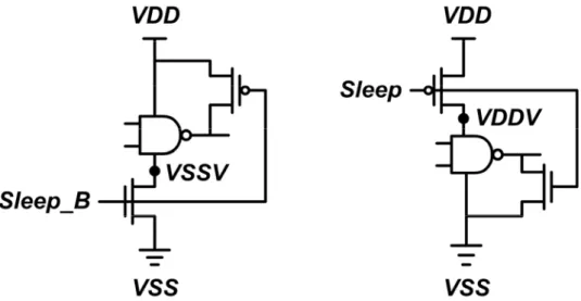
(64) Appendix. Supplementary of Power Gating Cell. Appendix Supplementary of Power Gating Cell In this Appendix, the characteristics of different power gating cells will be supplemented. The use of header and footer with NMOS and PMOS as a power switch depends on the overall floorplanning and performance consideration. The footer switch designs are reputed to be more sensitive to ground noise on the virtual ground (VSSV) coupled through the footer power switch. As a result, we will focus on the header approach in this Appendix and discuss the difference between NMOS and PMOS header designs.. Before a deeper analysis, we compare the operation mechanism between PMOS header and NMOS header. In Figure A-1, it is found that PMOS is turned on and off with the gate voltage switched to VSS and VDD+Vov, respectively, with the overdriven voltage Vov for further leakage reduction in the sleep state. Based on the same two-level voltages, VSS and VDD+Vov, we are going to illustrate the performance indices of NMOS and PMOS switches, and show the different features in NMOS and PMOS designs.. 54.
(65) Appendix. Supplementary of Power Gating Cell. Figure A-1: Power gating cell operation mechanism (a) PMOS header; (b) NMOS header. The PGC’s behavior is modeled as a resistor when it is turned on, acting as a gate between a permanent power supply (VDD) and a virtual power supply (VDDV). The VDDV value is required to approach the VDD voltage because a high voltage drop implies a larger power overhead dissipated in the PGC and smaller current driving force. This is illustrated in the point of view of the transconductance in an active transistor. According to the square-low model, the current of a NMOS transistor in the triode region is proportional to. I N ∝ μ N COX. W⎡ 1 (VGS − VTN )VDS − VDS2 ⎤⎥ ⎢ L⎣ 2 ⎦. (A-1). where μN is the electron mobility, Cox is the oxide capacitance, W and L are the width and length of a transistor, respectively. VTN is the threshold voltage of a NMOS transistor. VGS and VDS represent the voltage differences of gate-source and drain-source, respectively. Figure A-1 shows the configuration of header-style PGCs.. 55.
(66) Appendix. Supplementary of Power Gating Cell. In a power gating design, the correlation of voltage drop (VDD-VDDV) and driving current (IN) is concerned. We may further rewrite Equation A-1 as. I N ∝ μ N COX. W⎡ 1 (VOV + ΔV − VTN ) ΔV − ΔV 2 ⎤⎥ ⎢ L⎣ 2 ⎦. (A-2). where ΔV=VDS , VOV is the overdriven voltage relative to the VDDV level, and VGS =VOV +ΔV. Therefore, the transconductance of this NMOS transistor can be derived by the derivative of Equation A-2 with respect to ΔV.. gm, N =. ∂I N W ∝ μ N COX (VOV + ΔV − VTN ) ∂ΔV L. (A-3). To compare with the PMOS transistor, the transistor’s current is derived in a similar way except covering both the saturation and triode region. ⎧ ⎪⎪ μ P COX IP ∝ ⎨ ⎪μ C ⎪⎩ P OX. W L W L. 1 2⎤ ⎡ ⎢⎣(VSG − VTP ) VSD − 2 VSD ⎥⎦ (triode region) ⎡(V − V TP ⎣ SG. ). 2. ⎤ ⎦. (A-4). (saturation region). where μP is the electron mobility. We may further rewrite Equation A-4 with VSG and VSD replaced by VDD and ΔV, respectively. ⎧ ⎪⎪ μ P COX IP ∝ ⎨ ⎪μ C P OX ⎩⎪. W L W L. 1 ⎡ 2⎤ ⎢⎣(VDD − VTP ) ΔV − 2 ΔV ⎥⎦ (triode region) ⎡(VDD − V TP ⎣. ). 2. ⎤ ⎦. (A-5). (saturation region). In the PMOS transistor scheme, the change of gate voltage bellow VSS level has only slight increase of the IP current. Moreover, PMOS design can apply the second overdriven voltage for an improved leakage power saving. Therefore, we ignore the. 56.
(67) Appendix. Supplementary of Power Gating Cell. possible third voltage for a fair comparison between NMOS and PMOS designs. So, the transconductance of a PMOS transistor is. gm,P. W ⎧ ∂I P ⎪ μ P COX (VDD − VTP − ΔV ) (triode region) = ∝⎨ L ∂ΔV ⎪ (saturation region) ⎩0. (A-6). In comparison of IN and IP, there are two main differences and hence impacts to the mounted logic cells. First, IN is able to provide a larger driving current with a proper selection of the overdriven VOV value whereas IP current behavior is fixed when the VDD value is determined. Second, when logic cells are activated from the sleep state, i.e. ΔV =VDD to ΔV =0, the restored current of IP covers both the saturation and triode region whereas IN is only in the triode region. This implies that the saturated IP does not provide a larger current value when the voltage gap between VDD and VDDV becomes larger, whereas IN from a NMOS transistor does. Furthermore, the mobility value of μN is larger than μP, and this again guarantees that NMOS PGC is capable of providing larger driving current. To illustrate the driving current of NMOS and PMOS PGCs, the circuits are based on 90nm CMOS technology, and VDD and VOV are designed in 0.5V and 0.4V [14], respectively. The n- and p-MOSFET are sized in the same length and width, say 80nm and 0.6um. As a result, Figure A-2 shows the current and transconductance curves. In the current plot, the curves reflect the provided current pulling the VDDV from the stand-by level to VDD with different MOS threshold voltage, regular-VT (RVT) and high-VT (HVT). In the RVT-NMOS and PMOS curves, it is found that the driving current of RVT-NMOS is about an order higher than that of RVT-PMOS when ΔV =0.5V. This means RVT-NMOS provides 10x current at circuit’s wake-up instance. When the voltage drop ΔV approaches zero, the value becomes 1.3x difference, and. 57.
(68) Appendix. Supplementary of Power Gating Cell. RVT-NMOS current still remains higher than RVT-PMOS. Basically, the region around ΔV =0 implies the loaded circuits are active, so the current value represents the ability that the PGC can afford when a sudden large current is required without a voltage drop. On the other hand, in the region around ΔV =0.5V, it reflects that the circuits are in the sleep status, and the driving current corresponds to the provided value for circuit wakeup. As a result, it is shown that the ID value of the RVT-NMOS over ΔV =0~0.5V is larger than that of RVT-PMOS. This means a RVT-NMOS PGC provides better driving ability than a PMOS PGC either in active or sleep state. In the HVT-NMOS and PMOS, both of them has poorer driving force in terms of provided current than the RVT-NMOS and PMOS. If we look at the transconductance as shown in Figure A-2(b), it is also found that the RVT-NMOS possesses a higher gm value over the whole ΔV range. From the ID and gm plots, we are able to confirm that the use of RVT-NMOS as a power gating cell can take the advantage of smaller area overhead. In the following discussion and comparison, we denote the RVT-NMOS and RVT-PMOS as NMOS and PMOS for simplicity.. 58.
(69) Appendix. Supplementary of Power Gating Cell. Figure A-2: NMOS: VD(0.5V)+ VG(0.9V) and PMOS VS(0.5V)+ VG(0V) (a) driving current; (b) transconductance. To see the performance indices for NMOS and PMOS PGCs, a testing circuit of a ring oscillator is designed with the delay about 200ns at VDD=0.5V (without PGCs added) as illustrated in Figure A-3.. Figure A-3: Testing circuit. 59.
(70) Appendix. Supplementary of Power Gating Cell. To evaluate the performance of PGC with the circuit loads, NMOS and PMOS PGC designs are compared when testing circuit is in active and sleep state. In the active state, the gate voltage of PMOS PGC is fixed at 0V, whereas the gate voltage of NMOS PGC is varied from 0.8V to 1.2V to see the effect of overdriven gate voltage. Figure A-4 shows the VDDV value pulled up by the PGC with different widths. If we take 4% delay penalty as performance requirement, the corresponding PMOS PGC’s width is close to NMOS PGC with VOV 0.4V. When VOV is up to 0.5V, the required PMOS PGC width is 4x than NMOS one, and this means the PMOS PGC needs 4x area overhead to achieve the same performance requirement. Besides, when VOV is larger than 0.5V, the performance just increases slightly. Therefore, when the area overhead becomes a critical issue, the NMOS PGC with suitable overdriven gate voltage will be a better choice.. Active Mode 0.5. VDDV (V). 0.49. 0.48 NMOS Vov=0.3V 0.47. NMOS Vov=0.4V NMOS Vov=0.5V NMOS Vov=0.6V. 0.46. NMOS Vov=0.7V 0.45. PMOS 5. 10 PGC width (um). 15. 20. Figure A-4: VDDV pulled by PGC in the active state. 60.
數據
![Table 1-1: The power consumption, area, and cost of the quartz crystal [2] In-crystal 1μW~200μW](https://thumb-ap.123doks.com/thumbv2/9libinfo/8469528.183475/13.892.183.709.428.841/table-power-consumption-area-cost-quartz-crystal-crystal.webp)

+7


相關文件
In this thesis, we develop a multiple-level fault injection tool and verification flow in SystemC design platform.. The user can set the parameters of the fault injection
The purpose of this thesis is to propose a model of routes design for the intra-network of fixed-route trucking carriers, named as the Mixed Hub-and-Spoke
In this thesis, we propose a Density Balance Evacuation Guidance base on Crowd Scatter Guidance (DBCS) algorithm for emergency evacuation to make up for fire
In this paper, we discuss how to construct low-density parity-check (LDPC) codes, and propose an algorithm to improve error floor in the high SNR region by reducing the
This paper presents an integrated wireless network, rapid response to the three components of the Code (QRCode) and smart phones, build a low -cost "smart public bike
To maximize coverage rate and minimize overlapping sensing area, we propose a greedy algorithm to find an arc on the circumference of the minimum overlapping area which can
In this thesis, plentiful optimization analyses in order to obtain maximum displacement volumes for the external gear pumps are executed to find the optimal design parameters..
[22] Guillermo Gonzalez, Microwave Transistor Amplifier Analysis and Design: Chapter 4, Noise, Broadband, And High-Power Design Methods, New Jersey, Prentice Hall Inc,
