A New Approach to Constructing Optimal Prefix Circuits with Small Depth
Yen-Chun Lin* and Jun-Wei Hsiao**
*Dept. of Computer Science and Information Engineering
**Dept. of Electronic Engineering
National Taiwan University of Science and Technology, Taipei 106, Taiwan
E-mail: yclin@computer.org
Abstract
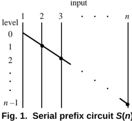
shown. A serial prefix circuit S(n) is shown in Fig.1, in which vertical edges from left to right are named line 1, line 2,..., line n, respectively. Input nodes are Prefix computation has many applications, and
on the top of a circuit and have indegree 0 and should be implemented as a primitive operation.
outdegree 1, representing input items. Output nodes Many combinational circuits for performing the prefix
are at the bottom and have indegree 1 and outdegree 0, operation in parallel, called parallel prefix circuits,
representing outputs. An operation node, represented have been designed and studied. The size of a prefix
by a black dot, performs the ⊗ operation on its two circuit D, s(D), is the number of operation nodes in
inputs, having indegree 2 and outdegree 1 or more. For D, and the depth of D, d(D), is the maximum level of
any operation node on line i at level j, its left input is operation nodes in D. Smaller depth implies faster
from a node at level j – 1, while its right input is computation, while smaller size implies less power
always from line i. A duplication node has indegree 1 consumption and smaller area in VLSI implementation
and outdegree 2 or more; it outputs multiple copies of and thus less cost. D is depth-size optimal if d(D) +
its single input. In Fig. 1, a duplication node is on line s(D) = 2n – 2. Another circuit parameter is fan-out.
1 at level 0. The numbers at the left of a prefix circuit A circuit having a smaller fan-out is faster and
denote the depth levels of the nodes to the right. The smaller in VLSI implementation. Thus, a circuit
input node on line i represents input xi. When no should have a small fan-out for it to be of practical
use. In this paper, we take a new approach to confusion is caused, we may use simply D for any designing a depth-size optimal parallel prefix circuit, prefix circuit D (p), where p may be the number of WE4, with fan-out 4 and small depth. In many cases inputs or a parameter with another meaning.
of n, WE4 has the smallest depth among all known prefix circuits. 1 2 3 level 1 2 n n –1 . . . . . . . . . input 0
1. Introduction
Given n values x1, x2,
...
, xn and an associative binary operation ⊗, the prefix operation is to compute the n values x1 ⊗ x2 ⊗...⊗ xi, 1 ≤ i ≤ n . Prefix computation has many applications, such as sorting, job scheduling, loop parallelization, and processor allocation [1, 2, 7-9, 17]. Because of its usefulness, itFig. 1. Serial prefix circuit S(n).
should be implemented as a primitive operation [3]. Many combinational circuits for performing the prefix
The size of a prefix circuit D , s ( D ), is the operation in parallel, called parallel prefix circuits,
number of operation nodes in D, and the depth of D , have been designed and studied [2, 4, 5, 8-11, 13-16].
d(D), is the maximum level of operation nodes in D. In this paper, we assume that the number of inputs
Smaller depth implies faster computation. Smaller is n, unless otherwise stated. We represent a prefix
size implies less power consumption and smaller area circuit with a directed acyclic graph containing n in VLSI implementation and thus less cost. Therefore, input nodes, n output nodes, at least n – 1 operation size and depth are important parameters of prefix nodes, and at least one duplication node. For ease of circuits. For any prefix circuit D, d (D ) + s(D ) ≥ presentation, in this paper, all the directed edges are 2 n – 2 [16]. Thus, D is depth-size optimal, or assumed to be downward; thus, the arrows need not be optimal for short, if d (D ) + s (D ) = 2n – 2. For
example, Fig. 1 shows that s (S ) = d (S ) = n – 1; Prefix circuit Q (n) with fan-out at most 4 has
thus, S is optimal. been presented in [14].
A third important parameter is fan-out. The fan-out
Property 1 [14]:
The depth of Q(n) is of a node is its outdegree. A node having a smaller
lgn if n ≤ 7, fan-out is faster and smaller in VLSI implementation
[18]. A node has unbounded fan-out if the fan-out is 2t – 4 if t ≥ 4 and 2t–1
≤ n < 3 × 2t–2
, not fixed and is a function of n; otherwise, the fan-out
2t – 3 if t ≥ 4 and 3 × 2t–2 ≤ n < 2t. of the node is a constant, or is bounded. The fan-out of
W (n) is a prefix circuit defined with the following prefix circuit D , fo(D ), is the maximum fan-out of
operation nodes [11]: all nodes in D . For example, fo(S ) = 2. A circuit
has unbounded fan-out if one of its nodes has Gi = {(i + 1, i + 2)}, i = 1, 2,…, n – 2; unbounded fan-out. A circuit should have a small G
n–1 = {(1, i) | i = 2, 3,…, n}.
bounded fan-out for it to be of practical use.
For example, W (3) and W (4) are shown in Fig. 2. For ease of presentation, let i:j represent the result
By definition, d ( W ) = n – 1, s ( W ) = 2n – 3, of computing xi ⊗ xi+1 ⊗ ... ⊗ xj, where i ≤ j. We
ia(W) = n – 2, and l(W) = n – 1 . use ia(D ) = a to denote that line 1 of prefix circuit
D has a duplication node at level a and has no
1 2 3 4 3 2 1 1 2 3 2 1 W(3) W(4) 3 2 1 1 2 3 4 5 6
duplication nodes at any level less than a . In addition, we use l(D ) = b to denote that line n of D obtains 1:n at level b.
Many previous parallel prefix circuits are briefly reviewed in [11]. Some of them with smaller depth are in the following. L Y D is an optimal prefix circuit
with unbounded fan-out, whose depth is between Fig. 2. W(3), W(4), and W(3) • W(4). 2 l g n – 6 and 2 lg n – 3 [9]. M is also an
optimal prefix circuit with unbounded fan-out, whose 2.2. Composition of prefix circuits, size depth is between 2 lg n – 5 and 2 lg n – 3 [12]. optimality, and other properties
H4 is an optimal prefix circuit with fan-out 4, whose
depth is between 2 lg n – 5 and 2 lg n – 3 [11]. Assume that A (n
1) and B ( n2) are two prefix Z4 is an optimal prefix circuit with fan-out 4, whose
circuits with n1 and n2 inputs, respectively. A (n1) depth is between 2 lg n – 6 and 2 lg n – 3 [6].
In this paper, we introduce a new optimal parallel and B(n2) can be composed into a prefix circuit with prefix circuit, denoted as W E 4 , with fan-out 4. In n
1 + n2 – 1 inputs by merging the operation node that
many cases of n, it has the smallest depth among all
produces 1:n1 on line n1 of A (n1) with the first, if known prefix circuits. Section 2 briefly reviews
not unique, duplication node on line 1 of B(n2); the previous results. Sections 3 and 4 present prefix
circuits WL and W V , respectively; these circuits will resulting circuit is denoted by A (n1) • B (n2) [16]. be used in Section 5 to construct W E 4 . Section 6 For example, Fig. 2 also gives W(3) • W(4). Three or compares W E 4 with the optimal parallel prefix more prefix circuits can also be composed into a single circuits mentioned in the previous paragraph in some prefix circuit, and the composition operation is detail. Section 7 concludes this paper. associative.
Definition 2 [11]: For any prefix circuit A with n
2. Brief review of previous results
inputs, if i a ( A ) = a , l( A ) = b , and s ( A ) = 2n – 2 + a – b , then A is size optimal; we say that A is A prefix circuit D can be defined with sets of
SOPC(n, a, b). operation nodes at level i, i = 1, 2,... , d(D) [16]:
Property 3 [11]: Q(n) is SOPC(n, 0, lg n).
Gi = {(x , y ) | at level i on line y there
Property 4 [11]: W (n ) is S O P C (n , n – 2, n – is an operation node whose left input
is the output of a node on line x at 1) with fan-out n.
level i – 1}. Property 5 [11]: If A is S O P C ( n , 0, b ) and If (x, y) ∈ Gi, the corresponding operation node d(A) = b, then A is optimal.
can be denoted as (x, y)i. Property 6 [11]: If A ( n1) and B ( n2) are SOPC(n1, a , b ) and S O P C ( n2 , c , d ) ,
SOPC(n1 + n2 – 1, a , b – c + d ) with depth 1 2 3 6 9 0 1 12 13 4 15 6 17 8 920 1 22 3 24 25 max{d(A(n1)), d(B(n2)) + b – c}.
3. Size optimal prefix circuit WL
Prefix circuit WL(5) is defined with the following operation nodes: G1 = {(2, 3), (6, 7), (10, 11)}, G2 = {(3, 4), (7, 8), (11, 12)}, Fig. 4. WL(6). G3 = {(4, 5), (8, 9), (12, 13)}, As already mentioned, W A (5) • W B (5) is G4 = {(5, 9)}, SOPC(25, 6, 8), thus s(W A (5) • W B (5)) = 2 × 25 – 2 G5 = {(9, 13)}, + 6 – 8 = 46. Clearly, s ( W L (6)) = 47. That is, G6 = {(1, 5), (1, 9), (1, 13)}, s(W L (6)) = 2 × 25 – 2 + 6 – 7. Since ia(W L (6)) = 6 and l ( W L (6)) = 7, by Definition 2, W L (6) is G7 = {(1, 2), (1, 3), (1, 4), (5, 6), (5, 7), (5, 8),
SOPC(25, 6, 7). (9, 10), (9, 11), (9, 12)}.
The above method of obtaining WL(6) from WL(5) Fig. 3 shows that d (W L (5)) = 7, fo(W L (5)) = 4, can be generalized to derive W L (t + 1) from W L (t), i a ( W L (5)) = 5, and l( W L (5)) = 6. In addition,
t ≥ 5.
s(W L (5)) = 23 = 2 × 13 – 2 + 5 – 6. Therefore, by Algorithm A: Let N be the set of nodes at levels Definition 2, WL(5) is SOPC(13, 5, 6).
t + 1 through 2t – 3 of W L (t), where t ≥ 5. We can obtain WL(t + 1) by the following procedures. 1 2 3 4 5 6 7 3 4 5 6 7 8 2 9 10 11 12 13
1. Move down the operation node (1, 3 × 2t– 3 + 1)t+1 of W L (t) by 1 level to become (1, 3 × 2t– 3 + 1)t+2, and move down all the other operation nodes in N by 2 levels, resulting in W A (t). (If the left input of an operation node comes from a duplication node, then moving the operation node implies that the duplication node should also be moved accordingly.)
2. Move down all the operation nodes in N by 2 levels to obtain WB(t).
3. Delete node (3 × 2t–3
+ 1, 3 × 2t– 2 + 1)t+3 of the
Fig. 3. WL(5).
composed prefix circuit W A (t) • W B (t), and add 2 nodes (3 × 2t– 3 + 1, 3 × 2t– 2 + 1)t+ 1 and We can move the operation node (1, 13)6 of WL(5)
(1, 3 × 2t–2
+ 1)t+2, resulting in WL(t + 1). downward by 1 level to be (1, 13)7, and move the other
operation nodes at level 6 and level 7 downward by 2
Theorem 7: W L (t) is SOPC(3 × 2t– 3 + 1, t , t + levels, resulting in a new prefix circuit WA(5). Note
1) with depth 2t – 3 and fan-out 4, for t ≥ 5. that d (W A (5)) = 9, f o (W A (5)) = 4, and W A (5) is
Proof: This theorem can be proved by induction on
S O P C (13, 6, 7). We can also obtain W B (5) by
t. The proof is omitted because of space limitation. moving down all the nodes at levels 6 and 7 of WL(5)
by 2 levels. Clearly, d(W B (5)) = 9, fo(W B (5)) = 4,
4. Size optimal prefix circuit WV
and WB(5) is SOPC(13, 7, 8).
By Property 6, WA(5) • WB(5) is SOPC(25, 6, 8).
We can delete the operation node (13, 25)8 of WA(5) • Prefix circuit WV(5) is defined with the following W B (5), and then add operation nodes (13, 25)6 and operation nodes:
G1 = {(2, 3), (5, 6), (8, 9)}, (1, 25)7, obtaining WL(6) as shown in Fig. 4. Clearly,
d (W L (6)) = 9, fo(W L (6)) = 4 and ia(W L (6)) = 6. G2 = {(3, 4), (6, 7), (9, 10)}, Since only operation nodes on line 25 are modified and G
3 = {(4, 7)}, W L (6) obtains 1:25 at level 7, clearly W L (6) is a
G4 = {(7, 10)}, prefix circuit and l(WL(6)) = 7.
G6 = {(1, 2), (1, 3), (4, 5), (4, 6), (7, 8), (7, 9)}. by Definition 2, WV(6) is SOPC(19, 5, 6).
The above method of obtaining WV(6) from WV(5) Fig. 5 shows that d(W V (5)) = 6, fo(W V (5)) = 4,
can be generalized to derive W V (t + 1) from W V (t), i a ( W V (5)) = 4, and l( W V (5)) = 5. In addition,
t ≥ 5. s(W V (5)) = 17 = 2 × 10 – 2 + 4 – 5. Therefore, by
Algorithm B: Let N be the set of nodes at levels Definition 2, WV(5) is SOPC(10, 4, 5).
t through 2t – 4 of W V (t), where t ≥ 5. We can obtain WV(t + 1) by the following procedures.
1 2 3 4 5 6 3 4 5 6 7 8 1 2 9 10
1. Move down the operation node (1, 9 × 2t–5
+ 1)t of W V (t) by 1 level to become (1, 9 × 2t– 5 + 1)t+ 1, and move down all the other operation nodes in N by 2 levels, resulting in VA(t).
2. Move down all the operation nodes in N by 2 levels to obtain VB(t).
3. Delete the node (9 × 2t– 5
+ 1, 9 × 2t– 4 + 1)t+ 2 of the composed prefix circuit V A (t) • V B (t), and add operation nodes (9 × 2t– 5
+ 1, 9 × 2t– 4 + 1)t
Fig. 5. WV(5).
and (1, 9 × 2t–4
+ 1)t+1, resulting in WV(t + 1). We can move down the operation node (1, 10)5 of
Theorem 8: W V (t) is SOPC(9 × 2t– 5 + 1, t – 1, W V (5) by 1 level to be (1, 10)6, and move the other
t) with depth 2t – 4 and fan-out 3, for t ≥ 6.
operation nodes at level 5 and level 6 downward by 2 Proof: This theorem can be proved by induction on levels, resulting in a new prefix circuit VA(5). Note t. The proof is omitted because of space limitation. that d ( V A (5)) = 8, f o ( V A (5)) = 3, and V A (5) is
S O P C (10, 5, 6). We can also obtain V B (5) by
5. Depth-size optimal prefix circuit WE4
moving down all the nodes at levels 5 and 6 of WV(5)by 2 levels. Clearly, d (V B (5)) = 8, fo(V B (5)) = 4,
For ease of presentation, let W G (t) = W L (t) • and VB(5) is SOPC(10, 6, 7). W L ( t – 1) • ... • W L (5) • W (4), for t ≥ 5, and
By Property 6, VA(5) • VB(5) is S O P C (19, 5, 7).
WG(4) = W(4). We can delete the operation node (10, 19)7 of VA(5) •
Lemma 9: W G (t) is SOPC(3 × 2t– 2 – 8, t , 2t – V B (5), and then add operation nodes (10, 19)5 and 3) with depth 2t – 3, for t ≥ 5.
(1, 19)6, obtaining WV(6) as shown in Fig. 6. Clearly,
Proof: By Theorem 7, WL(t) is SOPC(3 × 2t– 3 + d (W V (6)) = 8, fo(W V (6)) = 3, and ia(W V (6)) = 5. 1, t , t + 1) with depth 2t – 3. By Property 6, Since only operation nodes on line 19 are modified and
W L (t) • W L (t – 1) is S O P C (3 × 2t– 3 + 3 × 2t – 4 + W V (6) obtains 1:19 at level 6, clearly W V (6) is a
1, t, t + 2) with depth 2t – 3. Using Property 6 prefix circuit and l(WV(6)) = 6.
repeatedly, we can obtain that W L (t) • W L (t – 1) •...• WL(5) is SOPC(3 × 2t– 3 + 3 × 2t– 4 +…+ 3 × 22 1 2 3 4 5 6 3 4 5 6 7 8 1 2 9 10 7 8 11 12 13 14 15 16 17 18 19 + 1, t, 2t – 4), i.e., S O P C (3 × 2t– 2 – 11, t, 2t – 4), with depth 2t – 3. Since W (4) is SOPC(4, 2, 3) with depth 3, by Property 6, W G (t) = W L (t) • W L (t – 1) •...• W L (5) • W (4) is S O P C (3 × 2t– 2 – 8, t, 2t – 3)
with depth 2t – 3. Q.E.D.
Assume that n ≥ 21 and t = lg n, we define n-input prefix circuit WE4(n) as follows:
1. When 21 ≤ n ≤ 28 or 63 ≤ n ≤ 64, WE4(n) = Q(n – 21 × 2t–5 + 9) • WV(t) • Fig. 6. WV(6). WG(t – 1). 2. When 29 ≤ n ≤ 32; Since V A (5) • V B (5) is S O P C (19, 5, 7), s(V A ( 5 ) 37 × 2t–5 – 9 ≤ n ≤ 5 × 2t–2 – 8, t ≥ 6; or • VB(5)) = 2 × 19 – 2 + 5 – 7 = 34, Thus, s(WV(6)) = n = 7 × 2t–2 – 9, t ≥ 5, s ( V A (5) • V B (5)) – 1 + 2 = 2 × 19 – 2 + 5 – 6. WE4(n) = Q(n – 3 × 2t–2 + 8) • S(2) • WG(t). Furthermore, since ia(W V (6)) = 5 and l(W V (6)) = 6,
3. When 48 ≤ n ≤ 62; Case 8: When 7 × 2t– 3 – 8 ≤ n ≤ 2t , where t ≥ 7, 5 × 2t–3 – 7 ≤ n ≤ 7 × 2t–3 – 10, t ≥ 6; let m = n – 3 × 2t–3 + 9. 7 × 2t–3 – 8 ≤ n ≤ 2t , t ≥ 7; or Case 9: When 2t–1 < n ≤ 9 × 2t– 4 – 10, where t ≥ 2t < n ≤ 9 × 2t–3 – 10, t ≥ 7, 8, let m = n – 3 × 2t–4 + 9. WE4(n) = Q(n – 3 × 2t–3 + 9) • WG(t – 1). Case 10: When 9 × 2t– 4
– 9 ≤ n ≤ 37 × 2t– 6 – 10, 4. When 9 × 2t–4
– 9 ≤ n ≤ 37 × 2t–6
– 10, t ≥ 8, where t ≥ 8, let m = n – 21 × 2t–6
+ 9. WE4(n) = Q(n – 21 × 2t–5 + 9) • WV(t – 1) By Case 2, when 29 ≤ n ≤ 32, we have d(W E 4 )
• WG(t – 2). = 2 lg n – 3. By Cases 1, 3, 4, 7, and 8, when 21 ≤ As an example, Fig. 7 shows WE4(27). n ≤ 28, 47 ≤ n ≤ 64, or 7 × 2t– 3
– 9 ≤ n ≤ 2t , where t ≥ 7, we have d (W E 4 ) = 2 lg n – 4. By Case 6, 3 5 6 9 0 1 12 3 4 15 1 2 3 4 5 6 16 7 18 9 20 21 2 23 4 5 26 7 when t = 6, 33 ≤ n ≤ 46, we have d ( W E 4 ) = 2 lg n – 5. By Cases 5 and 6, when 37 × 2t– 6
– 9 ≤ n ≤ 7 × 2t– 3 – 10, where t ≥ 7, we have d (W E 4 ) = 2 lg n – 5. Finally, by Cases 9 and 10, when 2t– 1
< n ≤ 37 × 2t– 6
– 10, where t ≥ 8, we have d(W E 4 )
Fig. 7. WE4(27) = Q(15) • WV(5) • W(4).
= 2 lg n – 6.
As already mentioned, the fan-out of Q is at most Theorem 10: WE4(n) is an optimal prefix circuit
4 and the fan-out of W V (5) is 4. By Theorem 8, the with fan-out 4 and depth
fan-out of W V (t) is 3, t ≥ 6. By Property 4 and 2 lg n – 3 when 29 ≤ n ≤ 32;
Theorem 7, the fan-out of W (4) and WL is 4, Hence, 2 lg n – 4 when 21 ≤ n ≤ 28, 47 ≤ n ≤ 64, or
WE4(n) has a fan-out of 4. Q.E.D.
7 × 2t–3
– 9 ≤ n ≤ 2t
, where t ≥ 7; 2 lg n – 5 when 33 ≤ n ≤ 46 or 37 × 2t–6
– 9
6. Comparisons of optimal prefix circuits
≤ n ≤ 7 × 2t–3
– 10, where t ≥ 7;
For easy and exact comparisons, Table 1 gives the 2 lg n – 6 when 2t–1 < n ≤ 37 × 2t–6 – 10,
numbers of inputs that can be processed by where t ≥ 8.
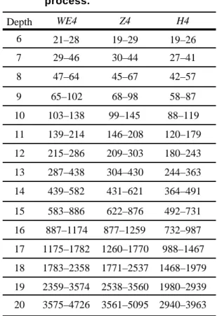
representative optimal parallel prefix circuits with Proof: The proof is through distinguishing 10 cases. specific depths. From Table 1, for n ≥ 21, d(WE4) ≤ Because the processes for the cases each are very
d(H4); that is, WE4 is better than H4. similar, we will give details for the first case only and Also from Table 1, when n = 29, 65 ≤
n ≤ 67, 139 give tips for the others. ≤ n ≤ 145, 287 ≤ n ≤ 303, 583 ≤ n ≤ 621, 1175 ≤
n Case 1: When 21 ≤ n ≤ 28, let m = n – 12; thus 9 ≤ 1259, 2359 ≤
n ≤ 2537, or 4727 ≤ n ≤ 5095, we get ≤ m ≤ 16 and lg m = 4. By Property 1, d (Z 4 ) = d (W E 4 ) – 1; however, when 45 ≤ n ≤ 4 6 , we have 4 ≤ d(Q (m )) ≤ 6. By Property 3, 99 ≤ n ≤ 102, 209 ≤ n ≤ 214, 431 ≤ n ≤ 438, 877 ≤ Q ( m ) is S O P C ( m , 0, 4). As already n ≤ 886, 1771 ≤ n ≤ 1782, or 3561 ≤ n ≤ 3574, we mentioned, W V (5) is S O P C (10, 4, 5) with have d (W E 4 ) = d (Z 4 ) – 1; otherwise, d (W E 4 ) = depth 6. Thus, by Property 6, Q ( m ) •
d(Z4). W V (5) is S O P C (m + 9, 0, 5). Since W ( 4 )
We now compare WE4 with optimal prefix circuits is SOPC(4, 2, 3), by Property 6, WE4(n) =
with unbounded fan-out. It can be checked that Q (m ) • W V (5) • W (4) is S O P C (m + 12,
d ( W E 4 ) ≤ d ( M ) except when n = 29. As for 0, 6) with depth 6 = 2 lg n – 4. Finally,
L Y D , when 21 ≤ n ≤ 77, d (L Y D ) ≤ d (W E 4 ); when by Property 5, WE4(n) is optimal.
78 ≤ n ≤ 446, d (W E 4 ) ≤ d (L Y D ); when n ≥ 447, Case 2: When 29 ≤ n ≤ 32, let m = n – 16.
d (W E 4 ) < d (L Y D ). That is, although both M and Case 3: When 48 ≤ n ≤ 62, let m = n – 15.
LYD have unbounded fan-out, only when n is small, Case 4: When 63 ≤ n ≤ 64, let m = n – 33.
d(M ) and d(L Y D ) have some chances to be smaller Case 5: When 37 × 2t– 6
– 9 ≤ n ≤ 5 × 2t – 3 – 8,
than d (W E 4 ) by 1. Specifically, when n > 29, M where t ≥ 7, let m = n – 3 × 2t–3
+ 8. can be replaced by W E 4 ; when n > 77, L Y D can be Case 6: When 5 × 2t– 3 – 7 ≤ n ≤ 7 × 2t – 3 – 10, replaced by WE4. where t ≥ 6, let m = n – 3 × 2t–3 + 9. Case 7: When n = 7 × 2t– 3 – 9, where t ≥ 6, let m = n – 3 × 2t–3 + 8.
Table 1. The numbers of inputs that some
References
optimal parallel prefix circuits
with specific depths can [1] S.G. Akl, Parallel Computation: Models and Methods ,
process. Prentice-Hall, Upper Saddle River, NJ, 1997.
[2] A. Bilgory and D.D. Gajski, "A heuristic for suffix Depth WE4 Z4 H4 solutions," IEEE Trans. Comput. , vol. C-35, Jan. 1986,
pp. 34-42.
6 21–28 19–29 19–26 [3] G.E. Blelloch, "Scans as primitive operations," I E E E
Trans. Comput. , vol. 38, Nov. 1989, pp. 1526-1538.
7 29–46 30–44 27–41 [4] R.P. Brent and H.T. Kung, "A regular layout for parallel adders," IEEE Trans. Comput., vol. C-31, Mar. 1982,
8 47–64 45–67 42–57
pp. 260-264.
9 65–102 68–98 58–87 [5] D.A. Carlson and B. Sugla, "Limited width parallel prefix circuits," J. Supercomput. , vol. 4, June 1990, pp.
10 103–138 99–145 88–119 107-129.
[6] J.-N. Chen, Constructing Depth-Size Opimal Parallel 11 139–214 146–208 120–179 Prefix Circuit Z4 , Master Thesis, Dept. of Electronic
Engineering, National Taiwan University of Science
12 215–286 209–303 180–243 and Technology, 2001.
[7] C.P. Kruskal, L. Rudolph, and M. Snir, "The power of 13 287–438 304–430 244–363
parallel prefix," IEEE Trans. Comput. , vol. C-34, Oct.
14 439–582 431–621 364–491 1985, pp. 965-968.
[8] R.E. Ladner and M.J. Fischer, "Parallel prefix 15 583–886 622–876 492–731 computation," J. ACM , vol. 27, Oct. 1980, pp.
831-838.
16 887–1174 877–1259 732–987 [9] S. Lakshmivarahan and S.K. Dhall, P a r a l l e l
Computing Using the Prefix Problem, Oxford
17 1175–1782 1260–1770 988–1467 University Press, Oxford, UK,1994.
[10] Y.-C. Lin, "Optimal parallel prefix circuits with fan-out 18 1783–2358 1771–2537 1468–1979 2 and corresponding parallel algorithms," N e u r a l ,
Parallel & Scientific Computations , vol. 7, Mar. 1999,
19 2359–3574 2538–3560 1980–2939
pp. 33-42.
20 3575–4726 3561–5095 2940–3963 [11] Y.-C. Lin, Y.-H. Hsu, and C.-K. Liu, "Depth-size optimal parallel prefix circuits with fan-out 4 and small depth," in Proc. Int. Conf. on Parallel and Distributed
Computing, Applications, and Technologies , 2001, pp.
7. Conclusion
74-82.[12] Y.-C. Lin and C.-K. Liu, "Constructing optimal parallel In this paper, we have presented Algorithm A and prefix circuits," in Proc. National Computer Symp., Algorithm B for constructing size optimal prefix 1999, pp. C-313-320.
[13] Y.-C. Lin and C.-K. Liu, "Finding optimal parallel circuits W L and W V ; together with Q and W ,
prefix circuits with fan-out 2 in constant time," Inform. theses circuits can be used to compose depth-size Process. Lett. , vol. 70, May 1999, pp. 191-195.
optimal parallel prefix circuit W E 4 . With our new [14] Y.-C. Lin and C.-C. Shih, "Optimal parallel prefix approach, tedious and lengthy proofs are not required. circuits with fan-out at most 4," in Proc. 2nd IASTED W E 4 can replace all the other optimal parallel Int. Conf. on Parallel and Distributed Computing and
prefix circuits with fan-out 4 except for Z4. We have Networks , 1998, pp. 312-317.
seen that d (W E 4 ) may be greater than d (Z 4 ) by 1, [15] Y.-C. Lin and C.-C. Shih, "A new class of depth-size d (W E 4 ) may be less than d (Z 4 ) by 1, and in most optimal parallel prefix circuits," J. Supercomput., vol.
14, July 1999, pp. 39-52. cases of n, d(WE4) = d(Z4).
[16] M. Snir, "Depth-size trade-offs for parallel prefix computation," J. Algorithms, vol. 7, 1986, pp. 185-201.
Acknowledgment
[17] H. Wang, A. Nicolau, and K.S. Siu, "The strict timelower bound and optimal schedules for parallel prefix This research was supported in part by the National with resource constraints," IEEE Trans. Comput., vol. Science Council of the R.O.C. under contract NCS 45, Nov. 1996, pp. 1257-1271.
[18] N.H.E. Weste and K. Eshraghian, Principles of CMOS 89-2213-E-011-099.
VLSI Design: A System Perspective , 2nd ed.,