. .. . : ~ . ~ . . . ,
surface science
ELSEVIER Applied Surface Science 92 (1996) 372-377
Investigation of the dosage effect on the activation of arsenic-
and boron-implanted low-pressure chemical vapor deposition
(LPCVD) amorphous-silicon films
Fang-Shing Wang a, Meng-Jin Tsai b, Wen-Koi Lai
a,
Huang-Chung Cheng a,*
a Department o f Electronics Engineering and Institute o f Electronics, National Chiao Tung University, Hsinchu, Taiwan, ROC b United Microelectronics Corp., Hsinchu, Taiwan, ROC
Received 12 December 1994; accepted for publication 4 March 1995
Abstract
The dopant activation of arsenic- and boron-implanted low-pressure chemical vapor deposition (LPCVD) amorphous silicon (t~-Si) films, furnace-annealed with different annealing temperatures has been investigated. For the arsenic-implanted specimens with a dosage of 4 × 1014 cm -2, an increase of sheet resistance was observed with increasing annealing temperature for the temperatures range from 700 to 850°C. The reverse annealing phenomenon is attributed to dopant segregation at grain boundaries and becomes less marked with heavier doped films (2 × l015 cm-2). Consequently for a dosage of 1 X 1016 cm -2, the sheet resistance exhibits a monotonic decrease with increasing annealing temperature. As for the boron-implanted specimens, the reverse annealing phenomenon is not observed. It means that dopant segregation is not significant for boron-implanted films.
1. Introduction
Polycrystalline silicon (poly-Si) deposited by the low-pressure chemical vapor deposition (LPCVD) technique is extensively used in modern very-large scale integrated (VLSI) devices [1]. The doped poly- Si films are generally used as the interconnection lines between devices, gate electrode materials for MOSFETs, load resistors for SRAMs, and poly- emitter contacts for bipolar devices, etc. [2]. For the latter two applicatiolas, the required doping can be accomplished with precise control by use of ion implantation [3]. The activation of the doped poly-Si or t~-Si films has been achieved by using annealing
* Corresponding author. Fax: 886 35 724361.
techniques such as furnace annealing [4], rapid ther- mal annealing [5], as well as laser annealing [6]. Both the As + and B ÷ are generally used as the n-type and p-type dopants in Si processing. In this paper, the furnace annealing of As +- and B÷-im - planted a-Si films has been investigated. With the annealing temperature varying from 600 to 1100°C, the dosage effects of the specimens for the different annealing temperatures have been observed and dis- cussed.
2. Experimental procedures
Three inch diameter, (100) oriented, n-type sili- con wafers were used as the substrates. After a field
0169-4332/96/$15.00 © 1996 Elsevier Science B.V. All rights reserved
F.-S. Wang et a l . / Applied Surface Science 92 (1996) 372-377 373 I ¢ ° m , . ¢ r.l'] z0 5 1¢ zo 3 ~ ' • As/4EI4 ' , \ - -=- -As/2EI5 '
~.~* _~-,..,,
. . - . - A . . • 1 1 1 0 2 , t , l h I , I , I t I , I . t , i , i . 600 700 800 900 I(X]0 1100 Annealing Temperature ( ' C )Fig. 1. Sheet resistances o f the As+-implanted specimens annealed at different temperatures. 10' ,-;,. • B/4EI4 - - . - - B/2EI5 --A-.- B/1 E l 6 1 0 2 , t , t , I , t , I , I , t , I , I , I , 6 0 0 7 0 0 8 0 0 9 0 0 1 0 0 0 1 1 0 0 Annealing Temperature ( ' C )
Fig. 2. Sheet resistance o f the B + - i m p l a n t e d specimens annealed at different temperatures.
oxide was thermally grown, an undoped a-Si film of thickness 100 nm was deposited by LPCVD at 550°C. The samples were As+-implanted at an energy of 70 keV or B+-implanted at an energy of 15 keV to the dosages of 4 × 10¹⁴, 2 × 10¹⁵, and 1 × 1016 cm -2, respectively. After cleaning, the samples were capped with a layer of 200 nm PECVD oxide to prevent dopant outdiffusion in the subsequent annealing pro- cess. The specimens were furnace-annealed in N 2 ambient for 1 h in the temperature range from 600 to 1100°C to study dopant activation at different tem- peratures. The encapsulation oxide was then dipped in a dilute HF solution. The sheet resistance, effec-
five carrier concentration, and electron mobility of the annealed poly-Si films were determined by the four-point probe and the Hall measurement appara- tus. Transmission electron microscope (TEM) obser- vations of these annealed specimens were performed to find the microstructure of poly-Si grains.
3. Results and discussion
Fig. 1 shows the curves of the sheet resistance versus the annealing temperature in the range from
A-" o o t _ -,-- L 102~ 10 ~° , i 600 C a r r i e r C o n c e n t r a t i o n H a l l Mobolity - - o -- A s / 4 E I 4 ~ As/4E14 - - * - - A s / 2 E I 5 • As/2E15 - -A -- A s / l E l 6 ~ As/1E16 ~ , . . _ ~ . - - ' A " ' ' ' A o A " " . . ° . O - - O ' ' - O - . . , O i , i i , I ' t , i i , J I i 700 800 900 1000 1100 Annealing Temperature (*C) 100 o ft. P ~ 10 ~ "
374 F.-S. Wang et al./Applied Surface Science 92 (1996) 372-377
600 to 1100°C for various As + implantation dosages. It is seen that for an annealing temperature below 700°C, the extremely high value of the sheet resis- tance implies inactivation of the implanted ions. The sheet resistances of the 1 × 1016 cm -2 samples show a monotonous decrease with increasing annealing temperatures above 700°C. For the specimens with the 2 × 1015 cm -2 dose, it is seen that between 700 and 8000C, the sheet resistance increases with in- creasing annealing temperature. This reverse anneal- ing phenomenon becomes even more marked for the 4 × 1024 cm -2 implanted film, which has a maxi- mum sheet resistance at the annealing temperature of 850°C. As for the B+-implanted samples with the three kinds of dosages shown in Fig. 2, the sheet resistance monotonically decrease with increasing annealing temperatures. No reverse annealing phe- nomenon is found for the B +-doped ones.
To further study the dopant activation of the implanted ions, the mobility and carder concentra- tion were also measured by the Hall measurement apparatus with the van der Pauw method. Figs. 3 and 4 show the carder concentrations and mobilities corresponding to the results shown in Figs. 1 and 2, respectively. For the As+-implanted samples, the carrier concentration of the 1 × 1026 cm -2 dose exhibits an increase with annealing temperature. However, the carrier concentrations of the 2 × 1025 cm-2 case decrease at first and then increase in the temperature range above 850°C. With regard to the
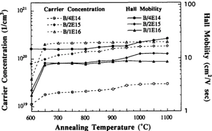
4 × 1014 cm -2 case, the carrier concentrations show a similar trend to the 2 × 1015 cm -2 ones but even- tually saturate when the annealing temperature ex- ceeds 1000°C. For the B+-implanted films with dif- ferent dosage, the carder concentrations increase, but the Hall mobilities decrease with increasing implan- tation dosage. As for the different annealing tempera- ture, carder concentrations and mobilities gradually increase and saturate above 1000°C for the three kinds of dosages.
The mobility is related to sheet resistance and carrier concentration. For a uniformly doped thin film, the sheet resistance (R s) can be expressed as
R s = 1 / ( N a q l X e f f t ) ,
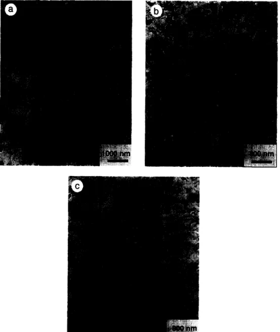
where q is the electronic charge, N a is the average carrier concentration, /Jeff is the effective carder mobility, and t is the film thickness. The sheet resistance increases when the carder concentration decrease exceeds the mobility increase and vice versa. This relationship also corresponds to the results shown in Fig. 4. The improvement in mobilities was examined by TEM observation. Figs. 5a, 5b, and 5c show the TEM observations of the films implanted by arsenic ions with the 2 × 10 Is cm -2 dose and annealed at 700, 800, and 1000°C for 1 h, respec- tively. In these photographs, it is found that the annealed samples with larger grain size and minor intragranular defects show higher mobility. It is also worth noting that the samples annealed at 1000°C
IO0
. - . 1 0 2z Carrier Concentration Hall Mobility ~ j ~ - - o - - B / 4 E 1 4 • B / 4 E I 4 • ~ - - # - - B/2EI5 * B/2EI5 .,~ , - , --A..BIIEI6 A B/IEI6 ° . . = 10 z° 10
L
I . " " 0 " " - ' 0 " - - 0 " " " 0 4,) ~ D ' " • ~ . 0 . - - 0 - ' ' O - - - O ' ' - O ' ' - m lOt9 600 700 800 900 1000 1100 A n n e a l i n g T e m p e r a t u r e (°C)F.-S. Wang et al./ Applied Surface Science 92 (1996) 372-377 375
show equiaxial grain structures with fewer microde- fects, which are obviously different from those films with dendritic grain structures annealed at lower temperatures. The structural differences of the speci- mens are attributed to different grain growth mecha- nisms under the different annealing temperatures [7]. Fig. 6 shows the microstructures of the films im-
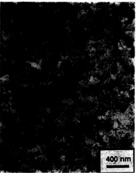
planted by B + with the 2 × 1015 cm -2 dose and annealed at 1000°C for 30 min. The microstructures of the films annealed at lower temperature also have a similar structure but a slightly smaller grain size than that annealed at 1000°C. The higher carrier mobility for the higher temperature is also realized for larger grain size.
Fig. 5. TEM photographs of films implanted by As + with the 2 × 10¹⁵ c m - 2 dose and annealed at (a) 700°C, (b) 800°C, and (c) 1000°C, respectively.
376 F.-S. Wang et a l . / Applied Surface Science 92 (1996) 372-377
Fig. 6. TEM photographs of films implanted by B + with the 2 × l0 ts cm -2 dose and annealed at 1000°C.
For the As-implanted samples, both dopant activa- tion and dopant segregation occur simultaneously in the annealing process. The former increases the car- der concentration and is influenced by the solid solubility of the poly-Si grains at the annealing temperature. The latter causes the activated dopants to diffuse to the poly-Si/SiO 2 interface or the grain boundaries and results in decrease of the carder concentration. The reverse annealing in the sheet resistances for the 2 × 1015 cm -2 specimens are attributed to the segregation of the activated dopants during annealing. It results in the decrease of the carder concentration from 700 to 850°C. The reverse tendency of the carrier concentrations at higher an- nealing temperatures is ascribed to the increasing intragranular solid solubility and the decreasing in- tragranular dopant segregation at higher tempera- tures. For the heavily implanted samples (the 1 X 1016 cm -2 case), since the amount of the segregated dopants is much less than the total dopant concentra- tion, the increase of the dopant activation with an- nealing temperature will be dominant, causing the monotonically decrease of the sheet resistance. With regard to the 4 X 10¹⁴ c m - 2 implanted films, the
reverse annealing becomes even more marked, indi- cating that the extent of dopant segregation is greater for the lower implantation dosage.
According to the carder trapping model [8], the carrier transport in poly-Si is influenced by potential barriers at the grain boundaries and the carder traps in intragranular microdefects. For the low-tempera- ture annealed samples, the microdefects in the grown grains cause the low electron mobility. With the release of microdefects due to higher annealing tem- peratures, the electron mobilities are thus promoted. Similarly, the higher electron mobilities for the 2 ×
l015 ¢m -2 for the 4 X 1014 cm -2 specimens are also attributed to lower potential barriers due to the higher carrier concentrations. However, the impurity scattering in the heavily doped films leads to lower electron mobilities for the 1 X 1016 cm -2 implanted ones.
The electrical properties (sheet resistance, carrier concentration, and mobility) which are monotonic functions of the annealing temperature show that dopant activation of the B +-implanted specimens is very different from annealed As +-implanted sam- ples. No reverse annealing phenomenon found im- plies that boron does not segregate at grain bound- aries or trap in microdefects. As the annealing tem- perature increases up above 1000°C, the saturation of carrier concentration results from the limit of the solid solubility of the B+-implanted a-Si films [1]. The excess boron in annealed samples form Si-B compounds or precipitate in the interior of grains and impurity scattering to influence the carrier transport. Such precipitation caused by heavily B + implanta- tion would suppress grain growth and therefore de- crease mobilities.
4. Conclusions
In summary, dosage dependence of the reverse annealing phenomenon for As+-implanted a-Si films has been observed. This phenomenon becomes more marked with decreasing implantation dosage. Dopant segregation causes the reduction of carrier concentra- tions for moderate doping levels, whereas the solid solubility becomes dominant for the heavily im- planted samples. As for the B+-implanted a-Si films,
F.-S. Wang et al./ Applied Surface Science 92 (1996) 372-377 377
the impurity scattering becomes dominant for carder transport. The dopants do not segregate at grain boundaries but may precipitate in the interior of grains when the dopant concentration exceeds its solid solubility.
Acknowledgements
This research was supported in part by the Repub- lic of China (ROC) National Science Council under Contract No. NSC 85-2215-E009-035. The technical support from the Semiconductor Research Center at National Chiao Tung University is acknowledged.
References
[1] T. Kamins, Polycrystalline Silicon for Integrated Circuit Ap- plications (Kluwer, Boston, 1988).
[2] T.H. Ning and R.D. Isaac, IEEE Trans. Electron Devices 32 (1980) 242.
[3] H. Ryssel, H. Ibcrl, M. Bleier, G. Prinkc, K. Haberger and H. Kranz, Appl. Phys. 24 (1981) 197.
[4] E.G. Lee and H.B. Ira, J. Electrochem. Soc. 138 (1991) 3465. [5] R.A. Powell and R. Chow, J. Electrochem. Soc. 132 (1985)
194.
[6] M.H. Juang and H.C. Cheng, Appl. Phys. Lett. 60 (1992) 2092.
[7] A. Nakamura, F. Emoto, E. Fujii, A. Yamamoto and Y. Uemoto, J. Appl. Phys. 66 (1989) 4248.