Improving Electrical Characteristics of Ta/Ta
2O
5/Ta
Capacitors Using Low-Temperature Inductively Coupled N
2O
Plasma Annealing
Kou-Chiang Tsai,a,bWen-Fa Wu,a,zChuen-Guang Chao,band Chi-Chang Wua,c a
National Nano Device Laboratories, Hsinchu, Taiwan b
Department of Materials Science and Engineering, and cInstitute of Nanotechnology, National Chiao Tung University, Hsinchu, Taiwan
The electrical characteristics of Ta/Ta2O5/Ta capacitors are improved by treatments with inductively coupled N2O plasma. A low-temperature共250°C兲 and short 共5 min兲 process was used to reduce the leakage current and improve the reliability. A low leakage current density共4.0 ⫻ 10−10A/cm2under 1 MV/cm兲, high breakdown field 共4.2 MV/cm at 10−6A/cm2兲, and lifetime of over 10 years at 1.61 MV/cm is obtained for the Ta/Ta2O5/Ta capacitor with the inductively coupled N2O plasma treatment. The conduction mechanism of the leakage current in the Ta/Ta2O5/Ta capacitor is discussed using current-voltage analyses and shows that the leakage current of the Ta/Ta2O5/Ta capacitor is dominated by Schottky emission. N2O plasma treatment can effectively reduce oxygen vacancies and the surface roughness of the Ta2O5film, inhibiting the conduction of the leakage current. © 2007 The Electrochemical Society. 关DOI: 10.1149/1.2719624兴 All rights reserved.
Manuscript submitted January 27, 2006; revised manuscript received January 26, 2007. Available electronically April 11, 2007.
There is an increased demand for high-performance capacitors for use as components of systems on chips共SoCs兲, which are essen-tial in realizing rf and mixed-signal integrated circuit共IC兲 applica-tions. Greater densities of the capacitors allow chips to be shrunk. Tantalum pentoxide 共Ta2O5兲 has a higher dielectric constant 共20– 25兲, lower leakage current, greater breakdown strength, and lower loss tangent than other dielectrics.1-3 However, the as-deposited Ta2O5films have a large leakage current and poor dielectric break-down. Several postannealing treatments have been suggested to im-prove the leakage currents of Ta2O5films.4Therefore, annealing is required to improve the electrical characteristics of Ta2O5. Conven-tional furnace annealing usually maintains samples at high tempera-tures for a long time, and so it is inappropriate for IC technology.
Tantalum共Ta兲 is cheaper than precious metals such as platinum 共Pt兲, palladium 共Pd兲, and their alloys that are responsible for a large part of the production cost of the capacitors. It is therefore a strong candidate to replace precious metal electrodes for ferroelectric and complex oxide thin-film-based devices. Additionally, it acts as an effective diffusion barrier at the connection between metals.5,6 In this paper, Ta was used as the electrode material for reactively sput-tered Ta2O5metal/insulator/metal共MIM兲 capacitors, and effects of the Ta electrode on the electrical and dielectric properties of Ta2O5 MIM capacitors were investigated.
One important mechanism of the leakage current is related to grain boundaries for Ta2O5 MIM capacitors. Although high-temperature annealing causes the as-deposited amorphous Ta2O5 film to crystallize into a polycrystalline film, it nevertheless gener-ates leakage currents because of the grain boundaries. Previous stud-ies have established that a polycrystalline Ta2O5film that has been annealed at high temperatures has a larger leakage current than an amorphous Ta2O5film.4,7However, problems associated with post-deposition annealing at a low annealing temperature for a short du-ration is unfavorable for the suppression in the leakage current,8as the oxidizing gases cannot be easily decomposed into oxygen atoms at low temperatures. This investigation introduces the advantages of post-treatment using an inductively coupled plasma 共ICP兲 system. Previous studies have revealed the use of an ICP system to deposit a dense dielectric film at low temperatures, typically as low as room temperature, with a very low chamber pressure in the 1–10 mTorr range.9-11ICP treatment was expected to improve the electrical char-acteristics of Ta2O5and ensure the reliability of the devices.
Experimental
Test capacitors with an MIM structure were fabricated on SiO2 共200 nm兲/Si substrates. The Ta bottom electrodes with a thickness of 200 nm were deposited onto SiO2/Si substrates by dc-magnetron sputtering using a highly pure tantalum target. After electrode depo-sition, 50 nm thick Ta2O5thin films were deposited by relative sput-tering. The sputtering chamber was evacuated to a base pressure of 1⫻ 10−7Torr. The films were prepared at a power of 100 W and a constant pressure of 3.5 mTorr. As-deposited Ta2O5films were sub-jected to various post-treatments to evaluate their effects. These were 共i兲 N2O plasma annealing at 250°C for 5 min in a plasma-enhanced chemical vapor deposition 共PECVD兲 system 共PE-N2O兲, 共ii兲 inductively coupled N2O plasma at 250°C for 5 min in a high-density plasma CVD system共ICP-N2O兲, 共iii兲 annealing in a quartz tube furnace in O2ambient at 400°C for 30 min共F-O2兲, and 共iv兲 no annealing treatment共reference兲. Conventional plasma was generated using an rf共13.56 MHz兲 power supply connected to a showerhead plate with a power of 300 W and a N2O flow rate of 200 sccm in a PECVD system. In the ICP system, an rf power source共13.56 MHz兲 is connected to the copper coil outside the ceramic plate of the upper chamber. The N2O flow rate was 200 sccm, the ICP power was 300 W, and the process pressure was 5 mTorr. 200 nm thick Ta films were deposited by sputtering and patterned using shadow masks to form top electrodes after post-treatments of Ta2O5films.
The thickness of the resulting Ta2O5 films was measured by scanning electron microscopy共SEM, JEOL JSM-6500F兲, which was also utilized to obtain the surface morphologies of the samples be-fore and after annealing treatments. The surface roughness was elu-cidated by atomic force microscopy 共AFM, Digital Instruments Nano-Scope III兲. Secondary ion mass spectrometry 共SIMS, CAM-ECA IMS-5F兲 was employed to measure the relative atomic concen-tration and thus verify the variation in the composition. The electri-cal characteristics of the Ta2O5MIM capacitors vs electric field and time were determined. During the electrical measurements, the top electrode was biased while the bottom electrode was grounded. The time-dependent dielectric breakdown共TDDB兲 properties were ob-tained under constant voltage stress using a Hewlett-Packard共HP兲 4156B semiconductor parameter analyzer.
Results and Discussion
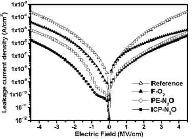
Figure 1 presents the leakage current densities of the reference, F-O2, PE-N2O, and ICP-N2O samples as a function of electric field up to ±4.5 MV/cm. Asymmetric curves are observed for current density vs electric field共J-E兲 characteristics. After post-treatments, the leakage current is more decreased at a negative bias than at a positive bias. The leakage current at negative bias is influenced
pri-z
marily by the interface of the Ta2O5 and Ta top electrode. The lowest leakage current densities were measured on the ICP-N2O sample, yielding a value of 4.0⫻ 10−10A/cm2at an electric field of −1 MV/cm, which is less than 3.8⫻ 10−9A/cm2for the PE-N2O sample, 3.8⫻ 10−7A/cm2 for the reference, and 5.7 ⫻ 10−8A/cm2for the F-O
2sample. Also, the leakage current den-sity of the ICP-N2O sample was lower than that in Ref. 12 at an electric field of 1 MV/cm. After the Ta2O5films were deposited, the oxygen escaped and oxygen vacancies were formed, according to
Oo↔ Vo⬙+ 2e−+1
2O2 关1兴
where Oo, Vo
⬙
, and e−represent the oxygen ion in its normal state, an oxygen vacancy, and an electron, respectively. A high concentration of oxygen vacancies caused electrons to be generated and a large leakage current to flow. Treatment with oxygen-containing plasma yielded active oxygen atoms and reduced oxygen vacancies and ul-timately improved the quality of Ta2O5films.Figure 1 indicates that the ICP-N2O and PE-N2O samples have better electrical characteristics than the F-O2sample. Many studies presented similar results and have established that the nitridation and oxidation are controlled by the mobility of nitrogen- and oxygen-based adatoms during the N2O plasma treatment.13-16N2O is a stronger oxidizing agent than O2because free O atoms are more easily produced according to the reaction16,17
O2→ 2 O 关2兴
e−+ N2O→ NO + N + e− 关3兴
N + NO→ N2+ O 关4兴
The activation energy in Eq. 2 is 5.12 eV, whereas that in Eq. 3 and 4 is 2.51 eV. This result can be easily explained by the fact that less energy is required to break the N–O bond in a N2O molecule than the OvO bond in an O2molecule. The excited oxygen atoms dif-fused rapidly into the Ta2O5films and reduced the degree of imper-fection and the concentration of oxygen vacancy. In addition, atomic N and surface-generated ions共NO兲 have been implicated in the ni-tridation process.
Figure 2 illustrates the SIMS depth profiles of the O elements in the F-O2 and ICP-N2O samples. The apparent oxygen diffusion found in the F-O2sample is because the oxygen atoms diffuse along the grain boundaries of the Ta crystal and react with the Ta bottom electrode layer during annealing. Nevertheless, almost no indication exists that oxygen atoms diffuse into the Ta bottom electrode layer in the ICP-N2O sample due to low-temperature plasma treatment.
The leakage current density in the ICP-N2O sample is much lower than that in the PE-N2O sample at a negative bias, as dis-played in Fig. 1. The influence of N2O plasma on the Ta2O5layer increases the concentration of oxygen atoms共or reduces the number of oxygen vacancies兲 in the Ta2O5 film. A PECVD system cannot generate high-density plasma. In fact, generating plasma even in a magnetic field at a chamber pressure of only a few mTorr is very difficult.18In an ICP system, a flowing rf current in the coils easily generates a changing magnetic field, which in turn induces a chang-ing electric field through inductive couplchang-ing. Therefore, the induc-tively coupled electric field accelerates electrons at low pressure. The electronic mean free path may be shorter than the gap between the electrodes, so enough ionizing collisions occur. Hence, induc-tively coupled plasma reactors produce a high electron temperature that efficiently dissociates the N2O gas under pressure and causes more O radicals and ions to be present. Previous studies demon-strated that the oxidant produced under high-density plasma dis-charge is more reactive than the primary reactant used in plasma O2 annealing.19 Accordingly, the high concentration of oxidants may explain why the leakage current density in the ICP-N2O sample is lower than that in the PE-N2O sample. Another reason may be the resulting roughness of the Ta2O5layer. The Ta2O5surfaces of the F-O2and PE-N2O samples are clearly rougher than that of the ICP-N2O sample, as displayed in Fig. 3. It is believed that the reactions or bombardments of energetic radicals and ions would occur during plasma treatment. They could sputter the films and make them smooth. The roughness effect can be interpreted as an image force that reduces the barrier height.20,21Table I summaries the electrical properties of Ta/Ta2O5/Ta capacitors with various post-treatments. The breakdown field is defined as the electric field when leakage current density exceeds 10−6A/cm2 under a negative bias. The breakdown fields of the reference and the F-O2samples are approxi-mately 1.2–1.9 MV/cm and that of the PE-N2O sample is 2.7 MV/cm. The excellent breakdown field of the ICP-N2O sample is 4.2 MV/cm. The improvement in breakdown field is attributed to the reduced surface roughness after treatments. A smooth surface can suppress the local accumulation of electrons and is responsible for the uniform electric field, and hence the ICP-N2O sample has a high breakdown field.
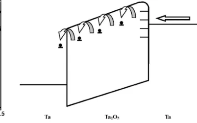
Figure 4 depicts the proposed schematic diagram of N2O plasma treatment on the Ta2O5 film based on the above results. Plasma treatment modifies the surface and causes ion bombardment effects. The principal dissociation products共N, O, and NO兲 of N2O would modify the surface of Ta2O5films. The O atoms were accelerated Figure 1. Leakage current densities of the Ta/Ta2O5/Ta capacitors before
and after various post-treatments. Figure 2. SIMS depth profiles of oxygen elements in Ta/Tators after furnace annealing at 400°C for 30 min and ICP treatment at 250°C2O5/Ta capaci-for 5 min.
toward the Ta2O5film, where they were adsorbed and incorporated in oxygen vacancies. The dissociation of gas importantly affects the results of plasma treatment. The leakage current density of the ICP-N2O sample is 1 order of magnitude lower than that of the PE-N2O
sample at an electric field of −1 MV/cm, because the concentration of oxygen vacancy is lower and the effect of nitridation is higher following ICP than PE treatment.
Figure 5 shows the leakage current density vs time characteris-tics at high stress electric fields. More than ten capacitors were measured for each post-treatment and one typical curve is shown in the study. At the beginning of the stress test, the leakage current fell rapidly. The decrease in the leakage current was believed to be caused by electron trapping.22,23The drop was gradual during the middle stage of the stress test. However, the leakage current rapidly increased and fatal breakdown occurred after the stress was applied for a longer period. Fatal breakdown is defined as the leakage cur-rent density increases to 10−3A/cm2 or ten times higher than the value at the previous 1 s time step. The data indicates that lower leakage films have longer breakdown lifetime. The ICP-N2O sample has a lower leakage current and longer breakdown lifetime under the stress at a constant electric field of 1.8 MV/cm. The leakage cur-rents in F-O2and PE-N2O samples are higher and associated with a shorter time to breakdown at constant fields of 1.2 and 1.6 MV/cm, respectively. Breakdown is manifested by the formation of a con-ductive path through the oxide initiated by the presence of weak spots.24Local field enhancements at the weak spots cause vacancy-related breakdown. The high-density local vacancies, including Figure 4. Schematic illustration for N2O plasma treatment on the Ta2O5 film.
Figure 5. Leakage current density vs time plots for F-O2 sample under 1.2 MV/cm, PE-N2O sample under 1.6 MV/cm, and ICP-N2O sample under 1.8 MV/cm.
Figure 3. 共Color online兲 AFM images of Ta2O5surfaces after共a兲 furnace annealing at 400°C for 30 min,共b兲 PE treatment at 250°C for 5 min, and 共c兲 ICP treatment at 250°C for 5 min.
traps, are responsible for vacancy-related breakdown. Furthermore, TDDB lifetime was studied under various equivalent electric fields. The ICP-N2O sample exhibits a longer term reliability than the PE-N2O, F-O2, and reference samples and the samples in Ref. 12. The extrapolated long-term lifetime demonstrates that the ICP-N2O sample can survive 10 years at a stress field of 1.61 MV/cm, as listed in Table I.
The leakage current in the Ta/Ta2O5/Ta capacitor may be due to several mechanisms, including Schottky emission, Poole–Frenkel effect, electronic hopping conduction, and tunneling.4,6,24,25The J-E characteristics of MIM capacitors are highly asymmetric with the voltage polarity for the Schottky emission. In this study, asymmetric
J-E characteristics were observed, as shown in Fig. 1. The Schottky
current is due to electrons which transit above the potential barrier at the surface of a metal or semiconductor and is typical of the electrode-limited current. A J-E relation for Schottky emission is given by the following equation4,6,25
J = AT2exp
冉
−q0kT
冊
exp冉

kTE
1/2
冊
关5兴where J is the current density, A is a constant, T denotes the absolute temperature, q is the electronic charge,0is the barrier height, k represents the Boltzmann constant, E represents the electric field, and is defined as
 =
冉
q3 40冊
1/2
关6兴 where0is the permittivity of free space and represents the high-frequency dielectric constant. Figure 6 shows the logarithmic cur-rent density as a function of the square root of the electric field 关log共J兲 vs E1/2兴. A good linearity is observed for the plots, indicating
that the Schottky emission is the possible dominant conduction mechanism for leakage currents, whereby electrons from the cath-ode overcome the Ta/Ta2O5energy barrier before being emitted into the Ta2O5. The Schottky emission can be explained as follows. When an electron enters the dielectric, it produces an image field that adds and lowers the barrier field, resulting in a reduced barrier height and an enhanced current given.
Figure 7 illustrates the conduction mechanism of the Ta/Ta2O5/Ta capacitor in the study. The Schottky emission is the possible dominant conduction mechanism for leakage currents. Sur-face roughness and oxygen vacancy are attributed to the resulting conduction mechanism. The F-O2sample has a rougher surface than the ICP-N2O sample, as shown in Fig. 3. It was reported that surface roughness yields on the image potential were as high as even 10–60% compared to that of a flat interface.21Some activated oxy-gen in the Ta2O5film could escape or diffuse into and react with the Ta bottom electrode layer during furnace annealing. The oxygen vacancy acts as an electron trap with certain trap level in the energy band diagram. The traps act as stepping sites for electrons and fa-cilitate their transport through the oxide. Moreover, the barrier height becomes low when the oxygen vacancies accumulate at the interface of the Ta2O5–metal electrode.6,26 ICP treatments cause more surface modification and less oxygen diffusion compared to furnace annealing treatments. The F-O2sample has a higher interfa-cial barrier compared to the ICP-N2O sample due to higher surface roughness and oxygen vacancy concentration. When the top elec-trode is negatively biased, electrons are relatively easily injected from the Ta top electrode into the tantalum oxide layer and further conductivity is governed via trap sites.
Conclusions
The electrical properties of Ta2O5thin films with MIM structures following the ICP-N2O post-treatments were examined. The result-Table I. Properties of Ta/Ta2O5/Ta capacitors with various post-treatments.
Reference F-O2 PE-N2O ICP-N2O
Roughness共nm兲 1.53 1.35 0.75 0.45
Leakage current共A/cm2兲 at E = 1 MV/cm 4.5⫻ 10−7 2.4⫻ 10−7 2.7⫻ 10−8 2.1⫻ 10−8 Leakage current共A/cm2兲 at E = −1 MV/cm 3.8⫻ 10−7 5.7⫻ 10−8 3.8⫻ 10−9 4.0⫻ 10−10 Breakdown field共MV/cm兲
at 10−6A/cm2under a negative bias 1.2 1.9 2.7 4.2
Breakdown field共MV/cm兲 at 10−6A/cm2under a positive bias
1.2 1.9 3 3.4
Dielectric constant ⬃19 20–23 19–21 19–21
Electric field of 10 year lifetime共MV/cm兲 0.87 1.23 1.61
Figure 6. The ln共J兲 vs E1/2plots for various Ta/Ta
2O5/Ta capacitors.
Figure 7. Schematic illustration of the conduction mechanism in the
ing Ta/Ta2O5/Ta capacitors have low leakage current densities 共4.0 ⫻ 10−10A/cm2 under 1 MV/cm兲, high breakdown fields 共4.2 MV/cm at 10−6A/cm2兲, and lifetimes of over 10 years at 1.61 MV/cm due to effectively dissociated N2O gas. The leakage current of the Ta/Ta2O5/Ta capacitor is dominated by Schottky emission. Oxygen vacancy and surface roughness are attributed to the resulting conduction mechanism in the study. The low-temperature ICP treatment reduces the diffusion of oxygen atoms into the Ta bottom electrode and lessens the oxygen vacancies, while the reactions of energetic radicals and ions reduce surface rough-ness. Consequently, the electrical characteristics and reliability of Ta/Ta2O5/Ta capacitors are enhanced after the low-temperature ICP treatments.
Acknowledgment
This work was financially supported by the National Science Council of the Republic of China under contract no. NSC 94-2215-E-492-009 and, in part, by the Ministry of Economic Affairs of the Republic of China under contract no. 95-EC-17-A-08-S1-0003.
National Nano Device Laboratories assisted in meeting the publication costs of this article.
References
1. T. P. Liu, W. P. Huang, and T. B. Wu, IEEE Trans. Electron Devices, 50, 1425 共2003兲.
2. J. W. Kim, S. D. Nam, S. H. Lee, S. J. Won, W. D. Kim, C. Y. Yoo, Y. W. Park, S. I. Lee, and M. Y. Lee, in Tech. Dig. - Int. Electron Devices Meet., 1999, 793. 3. J. Y. Tewg, Y. Kuo, J. Lu, and B. W. Schueler, J. Electrochem. Soc., 151, F59
共2004兲.
4. C. Chaneliere, J. L. Autran, R. A. B. Devine, and B. Balland, Mater. Sci. Eng., R.,
22, 269共1998兲.
5. W. F. Wu, K. L. Ou, C. P. Chou, and C. C. Wu, J. Electrochem. Soc., 150, G83 共2003兲.
6. K. C. Tsai, W. F. Wu, C. G. Chao, and C. P. Kuan, J. Electrochem. Soc., 153, G492 共2006兲.
7. T. Aoyama, S. Saida, Y. Okayama, M. Fujisaki, K. Imai, and T. Arikado, J.
Elec-trochem. Soc., 143, 977共1996兲.
8. W. R. Hitchens, W. C. Krusell, and D. M. Dobkin, J. Electrochem. Soc., 140, 2615 共1993兲.
9. J. M. Shieh, K. C. Tsai, and B. T. Dai, Appl. Phys. Lett., 81, 1294共2002兲. 10. K. C. Tsai, J. M. Shieh, and B. T. Dai, Electrochem. Solid-State Lett., 6, F31
共2003兲.
11. S. V. Nguyen, IBM J. Res. Dev., 43, 109共1999兲.
12. S. Ezhilvalavan and T. Y. Tseng, in Proceedings of the Electronic Components and
Technology Conference, p. 1042共1999兲.
13. S. C. Sun and T. F. Chen, IEEE Electron Device Lett., EDL-17, 355共1996兲. 14. K. C. Tsai, W. F. Wu, J. C. Chen, C. G. Chao, and T. J. Pan, J. Electrochem. Soc.,
152, G83共2005兲.
15. K. C. Tsai, W. F. Wu, J. C. Chen, C. G. Chao, and T. J. Pan, J. Vac. Sci. Technol.
B, 22共3兲, 993 共2004兲.
16. W. S. Lau, M. T. C. Perera, P. Babu, A. K. Ow, T. Han, N. P. Sandler, C. H. Tung, T. T. Sheng, and P. K. Chu, Jpn. J. Appl. Phys., Part 2, 37, L435共1998兲. 17. B. C. Smith, A. Khandelwal, and H. H. Lamb, J. Vac. Sci. Technol. B, 18, 1757
共2000兲.
18. Y. Vota, J. Hander, and A. A. Saleh, J. Vac. Sci. Technol. A, 18, 372共2000兲. 19. D. W. Hess, IBM J. Res. Dev., 43, 127共1999兲.
20. S. Blonkowski, M. Regache, and A. Halimaoui, J. Appl. Phys., 90, 1501共2001兲. 21. Y. S. Kim, Y. H. Lee, K. M. Lim, and M. Y. Sung, Appl. Phys. Lett., 74, 2800
共1999兲.
22. C. Chen, S. E. Holland, and C. Hu, IEEE Trans. Electron Devices, ED-32, 413 共1985兲.
23. S. Yamamichi, A. Yamamichi, D. Park, T. J. King, and C. Hu, IEEE Trans.
Elec-tron Devices, 46, 342共1999兲.
24. E. Atanassova, N. Novkovski, A. Paskaleva, and M.-P. Gjorgjevich, Solid-State
Electron., 46, 1887共2002兲.
25. S. M. Sze, Physics of Semiconductor Device, p. 402, Wiley, New York共1981兲. 26. J. H. Joo, Y. C. Jeon, J. M. Seon, K. Y. Oh, J. S. Roh, and J. J. Kim, Jpn. J. Appl.