This article was downloaded by: [National Chiao Tung University 國立交通大學] On: 24 April 2014, At: 19:33
Publisher: Taylor & Francis
Informa Ltd Registered in England and Wales Registered Number: 1072954 Registered office: Mortimer House, 37-41 Mortimer Street, London W1T 3JH, UK
Journal of the Chinese Institute of Engineers
Publication details, including instructions for authors and subscription information:
http://www.tandfonline.com/loi/tcie20
The influence of process parameters on
the structure and morphology of pulsed
plasma
‐polymerized octafluorotoluene films
Meng‐Dan Jiang a , Ling‐Yung Wang a , Hong‐Cheu Lin b , Ta‐Chin Wei c , Shih‐Hsien Yang c , Cheng‐Hsiang Chuang d & Tsung‐Pei Tseng d
a
Department of Materials Science and Engineering , National Chiao Tung University , Hsinchu 300, Taiwan, R.O.C.
b
Department of Materials Science and Engineering , National Chiao Tung University , Hsinchu 300, Taiwan, R.O.C. Phone: 886–3–5712121 ext. 55305 Fax: 886–3–5712121 ext. 55305 E-mail:
c
Department of Chemical Engineering and R & D Center for Membrane Technology , Chung Yuan Christian University , Chung Li, 32023, Taiwan, R.O.C.
d
Polymer Chemistry Section, Chemical System Research Division , Chung Shan Institute of Science & Technology , Lung Tan 325, Taiwan, R.O.C.
Published online: 04 Mar 2011.
To cite this article: Meng‐Dan Jiang , Ling‐Yung Wang , Hong‐Cheu Lin , Ta‐Chin Wei , Shih‐Hsien Yang , Cheng‐Hsiang
Chuang & Tsung‐Pei Tseng (2010) The influence of process parameters on the structure and morphology of pulsed plasma‐polymerized octafluorotoluene films, Journal of the Chinese Institute of Engineers, 33:7, 1075-1081, DOI:
10.1080/02533839.2010.9671696
To link to this article: http://dx.doi.org/10.1080/02533839.2010.9671696
PLEASE SCROLL DOWN FOR ARTICLE
Taylor & Francis makes every effort to ensure the accuracy of all the information (the “Content”) contained in the publications on our platform. However, Taylor & Francis, our agents, and our licensors make no
representations or warranties whatsoever as to the accuracy, completeness, or suitability for any purpose of the Content. Any opinions and views expressed in this publication are the opinions and views of the authors, and are not the views of or endorsed by Taylor & Francis. The accuracy of the Content should not be relied upon and should be independently verified with primary sources of information. Taylor and Francis shall not be liable for any losses, actions, claims, proceedings, demands, costs, expenses, damages, and other liabilities whatsoever or howsoever caused arising directly or indirectly in connection with, in relation to or arising out of the use of the Content.
This article may be used for research, teaching, and private study purposes. Any substantial or systematic reproduction, redistribution, reselling, loan, sub-licensing, systematic supply, or distribution in any
form to anyone is expressly forbidden. Terms & Conditions of access and use can be found at http:// www.tandfonline.com/page/terms-and-conditions
THE INFLUENCE OF PROCESS PARAMETERS ON THE
STRUCTURE AND MORPHOLOGY OF PULSED
PLASMA-POLYMERIZED OCTAFLUOROTOLUENE FILMS
Meng-Dan Jiang, Ling-Yung Wang, Hong-Cheu Lin*, Ta-Chin Wei, Shih-Hsien Yang, Cheng-Hsiang Chuang, and Tsung-Pei Tseng
ABSTRACT
This work describes amorphous fluorinated polymer films deposited by pulsed plasma polymerizations of octafluorotoluene (PPP-OFT) monomers on ITO glass as the hole-injection layer of organic electroluminescent (EL) devices, in order to study the influence of sample position and duty cycle on PPP-OFT film characteristics, and also to find a good process to yield a higher retention degree of monomers and lower roughness of OFT fluorocarbon films. Experimental results revealed that PPP-OFT films deposited at positions far away from the RF coil and close to the monomer inlet showed less roughness than films deposited near the high RF-flux regions. In addition, the retention of the monomers in the PPP-OFT layer will be high if the depo-sition is conducted near the monomer inlet but some distance away from the RF electrode. Moreover, amorphous fluorinated polymer films can be deposited with higher fluorine to carbon (F/C) ratios and CF2 contents at proper substrate positions by means of different sticking coefficients of free radicals dissociated by octafluo-rotoluene monomers.
Key Words: EL, pulsed plasma polymerizations, octafluorotoluene, hole-injection.
*Corresponding author. (Tel: 886-3-5712121 ext. 55305; Fax: 886-3-5724727; Email: linhc@cc.nctu.edu.tw)
M. D. Jiang, L. Y. Wang, and H. C. Lin are with the Department of Materials Science and Engineering, National Chiao Tung University, Hsinchu 300, Taiwan, R.O.C.
T. C. Wei and S. H. Yang are with the Department of Chemical Engineering and R & D Center for Membrane Technology, Chung Yuan Christian University, Chung Li 32023, Taiwan, R.O.C.
C. H. Chuang and T. P. Tseng are with the Polymer Chemistry Section, Chemical System Research Division, Chung Shan Institute of Science & Technology, Lung Tan 325, Taiwan, R.O.C.
I. INTRODUCTION
Many research groups have reported that the durability and efficiency of EL devices strongly de-pend on anode/organic interfaces (Van Slyke et al., 1996). The energy barriers at the interfaces between the anode and the hole-transporting layer (HTL) sig-nificantly influence the performance of EL devices. In order to deal with the above-mentioned pro-blems, it has been suggested that the formation of a
fluorocarbon layer between ITO and the HTL can improve ITO characteristics and hole injection. For example, a fluorocarbon film made of RF-plasma-polymered CFx (Hung et al., 2001), a UV-irradiated CFx film (Tong et al., 2004), a thermal-deposited Teflon film (Gao et al., 2003), or an evaporable fluoro-molecule film (POFDA) (Gao et al., 2004) all can function as buffer layers to improve hole injec-tion at the juncinjec-tion between ITO and the organic HTL. In the case of fluorocarbon films being used as buffer layers for EL devices, it is necessary to produce a film possessing a few-nm thickness and a smooth morphology. In view of the above-mentioned pro-blems, it is necessary to provide a good process for manufacturing a fluorocarbon film with improved hole-injection for an OLED device.
Amorphous fluorinated polymer film prepared by plasma polymerization of octafluorotoluene has been reported previously (Chan et al., 1999). The aim of the present work is to investigate the influ-ence of the sample position on deposition and the duty
1076 Journal of the Chinese Institute of Engineers, Vol. 33, No. 7 (2010)
cycle position on the PPP-OFT fluorocarbon film characteristics, and also to find a good process for pulsed plasma polymerization. Since the pulsed plasma polymerization processes have various depo-sition conditions, a series of plasma polymerization experiments for new monomers must be conducted in the deposition system in order to evaluate the ef-fects of the deposition conditions on the chemical structures of the resulting films. By utilization of an RF coil with a low pulsed frequency of 100 Hz and at various duty-cycles (power inputs), pulsed plasma po-lymerizations of octafluorotoluene, i.e., (C6F5)CF3, monomers were employed to synthesize PPP-OFT films at variable locations of the plasma reactor. Ac-cording to the literature on plasma polymerization using a pulsed plasma with a low power input (Tamirisa et al., 2004; Kinmond et al., 2005; Kim et
al., 2009), the retention of the monomers in the
syn-thesized films could be hyposyn-thesized to be high if the plasma films were deposited away from the RF elec-trode region. Our novel deposition technique of pulsed plasma polymerization yielded PPP-OFT films, which were deposited on oxygen-plasma-treated ITO, was expected to exhibit good adhesion, low moisture absorption, excellent transparency, and high thermal stability.
II. EXPERIMENTAL
Low-frequency (100 Hz) pulsed plasma poly-merizations of octafluorotoluene monomers at vari-ous distances away from the RF coil in the plasma reactor were used to synthesize PPP-OFT films. These PPP-OFT films were prepared on Si-wafer, glass, and ITO-glass substrates by low-temperature chemical vapor deposition (CVD) in an argon/ octafluorotoulene flow (4:1) atmosphere. The plasma apparatus (as shown in Fig. 2) consisted of a tubular reactor (internal diameter 6 cm, length 100 cm) with two external and capacitively coupled electrodes. The grounded (cold) electrode was placed at a distance 10 cm away from either side of the powered (hot)
electrode, while the samples were placed in different positions. After the reactor had been pumped to a pressure of around 34 mtorr, it was flushed with an oxygen flow (10 sccm) for 10 min. The samples were then treated with either a continuous or a pulsed plasma (13.56 MHz, 30 W, 10 sccm, 300 mtorr) for a predetermined time. The real distances away from the center P.1 of various sample codes, i.e. P.P, P.1, P.3, P.5, P.7, P.9, and P.10, of PPP-OFT layers were -5, 0, 5, 10, 15, 20 and 22.5 cm, respectively. The characteristics of the thin films were examined by X-ray photoelectron spectroscopy (XPS), Fourier trans-form infrared (FTIR) spectroscopy, and atomic force microscopy (AFM).
Volumetric flow rate is commonly measured in sccm (standard cubic centimeters per minute), which, in this study, was controlled by volatilizing oc-tafluorotoluene monomers into vapor, controlling the metering valve and calculating weight change of octafluorotoluene at constant pressure and temperature. Consequently, the flow rate calibration curve can be attained by controlling the metering valve in this experiment, and matching the control of the flow rate to the calibration curve. Accordingly, the calibration curve of the volumetric flow rate is represented by the following formula (1),
∆W
M ×∆t1 × 22400 = Flow rate (sccm), (1)
∆W : Weight change of C7F8 (g)
∆t : Time interval (min.)
M : Molecular weight of C7F8 (g/mole)
22400 : Volume of gas under the standard state (S.T.P.) (cm3/mole)
III. RESULTS
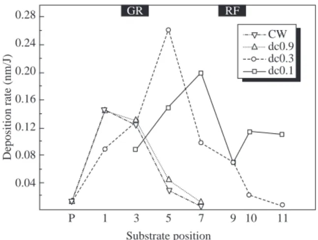
The PPP-OFT samples were treated in an argon/ octafluorotoulene plasma. Fig. 3 shows the deposi-tion rate (nm/min.) as a funcdeposi-tion of the substrate po-sition at various duty cycles. It can be seen that the deposition rate of PPP-OFT films rose with increas-ing duty cycle. In addition, with increasincreas-ing duty cycle, the maximum peak of the deposition curve transferred to the forward section of the reactor. This is the rea-son that the higher duty cycle enhances the plasma density, and the deposition rate rose, obviously, in this front area of the reactor. When the monomers reach the plasma zones, their concentrations become so low that there are not enough collisions with elec-trons (even if there are lots of high-energy elecelec-trons). Hence, the deposition rate in the rear area of reactor clearly falls. On the contrary, as duty cycles fall, the numbers of high-energy electrons dissociating from monomers in the front region are so insufficient as to induce extremely low deposition rates. Since
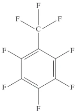
C F F F F F F F F
Fig. 1 Chemical structure of octafluorotoluene monomer
the numbers of high-energy electrons are enough to trigger plasma polymerization only in the neighbor-hood of plasma zones under this condition, the maxi-mum point of the deposition curve moves backward to those areas. Moreover, the curve revealed that the deposition rate of d.c. 0.1 declined abruptly in the vicinity of the RF electrode. This is the reason why the electrode has such a powerful self-bias voltage, which can attract and accelerate cations to etch the substrate by ion bombardment, That is to say, both deposition and etching on substrates occurred at the same time. Etching was especially noteworthy on substrates near the RF electrode. At position P.3, there is some etching at the ground electrode, but, not as apparent as that at the RF electrode by reason of the weaker bias voltage of the grounding electrode.
Figure 4 shows the deposition rate per joule (nm/joule) as a function of the substrate position at various duty cycles, where the maximum level of the deposition rate transferred to the forward section of various substrate positions was observed, and the depo-sition rate of PPP-OFT films rose with rising duty
cycles. Besides, the highest deposition rate is not at the greatest energy (average power), but at a duty cycle of 0.3. There are two possible explanations. On the one hand, the ion can etch the substrate by ion bom-bardment during the plasma polymerization, and deposition on substrates also can occur simultaneously under higher duty cycles. It is quite obvious that the ion etches the substrate by reason of the longer time of ion bombardment, thus the deposition rate (per joule) of a duty cycle of more than 0.3 drops consequently. On the other hand, the monomers dissociated previ-ously can deposit directly on substrates without elec-tron impingement, enhancing the deposition rate during the plasma off time period. When the plasma off time is too long, the deposition species in the gas phase will be consumed to a large extent, since there is no plasma to be triggered at this moment. Then, the free radicals dissociated from monomers are not formed, so there is no deposition and thus the deposition rate declines. Therefore, it is advisable that an optimum value of the plasma off time should be sought to carry out the plasma polymerization.
Ar, N2, O2 Monomer 13.56 MHz RF Generator Pumping System (300 mTorr) Matching network 10 cm MFC P 1 3 5 7 2 4 6 8 9 10 11 F F F F F F F F 280 240 200 160 120 80 40 0 P 1 3 5 Substrate position 7 9 10 11
Deposition rate (nm/min)
GR RF
CW dc0.9 dc0.3 dc0.1
Fig. 2 PECVD schematic diagram illustrating substrate positions in cylindrical glass reactor
Fig. 3 Deposition rate (nm/min) as a function of substrate
posi-tion at various duty cycles (C7F8/Ar = 1/4, 300 mTorr, 30
W) 0.28 0.24 0.20 0.16 0.12 0.08 0.04 P 1 3 5 Substrate position 7 9 10 11 Deposition rate (nm/J) GR RF CW dc0.9 dc0.3 dc0.1
Fig. 4 Deposition rate per joule (nm/joule) as a function of
sub-strate position at various duty cycles (C7F8/Ar = 1/4, 300
mTorr, 30 W)
1078 Journal of the Chinese Institute of Engineers, Vol. 33, No. 7 (2010)
Figure 5 shows the FTIR spectra of films deposited at different sample positions in the plasma reactor. When a pulsed plasma is applied, the IR peaks of carbon double bonds tend to disappear near the RF electrode (at sample position p.9). The in-creasing relative intensities of the absorption bands at 1500 and 980 cm–1 (farther away from the RF coil and near sample position p.p) are particularly significant, where the absorption band at 1500 cm–1 arises from the fluorinated aromatic ring vibrations but that at 980 cm–1 is associated with C-F (aromatic) stretching frequency. That is the reason why the den-sity of high energy electrons rises enhancing the prob-ability of electron and monomer collisions which will destroy the aromatic structures. In addition, the 1735 cm–1 and 1780 cm–1 peaks represent the absorption of CF = CF and CF2 = CF stretching vibrations, both of which can be attributed to C = C bond stretch caused by the ruptured benzene structures produced by the striking of plasma active species. Therefore,
the retention of the monomers in the PPP-OFT layer will be high if the deposition is conducted near the monomer inlet but some distance away from the RF electrode.
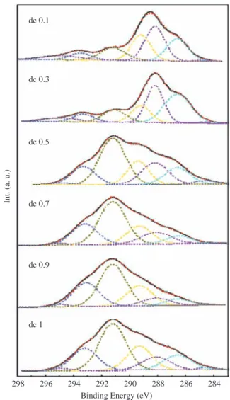
Figure 6 and Table 2 show the XPS C1s spectra of the PPP-OFT films at different duty cycles in the plasma reactor, which are deconvoluted into seven moieties to be arranged in the order of increasing
3000 2500 2000 1500 1000
Wavenumber (cm—1)
Absorbance (a. u.)
500 Octafluorotoluenc P.P P.1 P.3 P.5 P.7 P.10
Fig. 5 FTIR spectra of octafluorotoluene monomer and PPP-OFT
films polymerized by plasma processes (300 mtorr, 30 W, duty cycle 0.3) at different positions
298 296 294 292 290
Binding Energy (eV)
288 286 284
Int. (a. u.)
dc 0.1 dc 0.3 dc 0.5 dc 0.7 dc 0.9 dc 1
Fig. 6 XPS C1s spectra of PPP-OFT films polymerized by plasma
processes (300 mtorr, 30 W, sample position p.7) at dif-ferent duty cycles
Table 1 C1s bonding environment by XPS analysis of PPP-OFT films polymerized by plasma processes (300 mtorr, 30 W, duty cycle 0.3) at different positions.
Material C1s bonding environment (%) F/C C-C C-CFn CF CF2 CF3 C = C
PPP-OFT (p.9, Z = 20 cm) 0.97 19.34 51.23 15.8 5.03 7.58 0.981 PPP-OFT (p.5, Z = 10 cm) 0.85 21.25 51.60 14.74 3.64 7.66 0.920 PPP-OFT (p.3, Z = 5 cm) 1.04 23.66 47.00 15.89 4.59 7.82 0.926 PPP-OFT (p.1, Z = 0 cm) 0.63 32.48 35.96 20.63 5.55 4.76 0.939
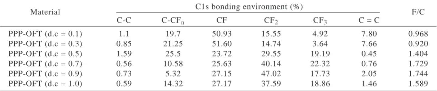
Table 2 C1s bonding environment by XPS analysis of PPP-OFT films polymerized by plasma processes (300 mtorr, 30 W, sample position p. 7) at different duty cycles.
Material C1s bonding environment (%) F/C
C-C C-CFn CF CF2 CF3 C = C PPP-OFT (d.c = 0.1) 1.1 19.7 50.93 15.55 4.92 7.80 0.968 PPP-OFT (d.c = 0.3) 0.85 21.25 51.60 14.74 3.64 7.66 0.920 PPP-OFT (d.c = 0.5) 1.59 25.5 23.72 29.55 19.19 0.45 1.404 PPP-OFT (d.c = 0.7) 0.56 10.58 25.63 40.14 22.32 0.76 1.729 PPP-OFT (d.c = 0.9) 0.73 5.32 27.15 47.02 17.73 2.05 1.744 PPP-OFT (d.c = 1.0) 0.59 14.32 27.17 37.59 18.86 1.46 1.589
duty cycle (from top to bottom). These seven chemi-cally distinct C atoms are assigned as follows.: -CF3 (293.3 eV), -CF2- (291.2 eV), -CF- (non-aromatic, 288 eV), -CF- (aromatic, 287.2 eV), C-C-F (285.2 eV), and C-C (284.6 eV). The broad peak from 291 to 296 eV corresponds to the shake-up of π bonds, arising from the aromatic rings in these films. Be-cause the average plasma power energy of duty cycle 0.3 is too low to crack monomers excessively, the chemical compositions of PPP-OFT films changing in concert with the substrate positions are not apparent. Compared with FTIR spectra in Fig. 5, they are not in conformity with XPS data (as shown in Table 1). It can be inferred that PPP-OFT films pre-pared by the ion bombardment at substrate positions close to the plasma zones produce more dangling bonds and the octafluorotoluene monomers will also react with those dangling bonds on the surfaces of PPP-OFT films during the plasma off periods, lead-ing to thin films includlead-ing higher retention degrees of monomers. Due to the dissimilarity of the surface and bulk composition of PPP-OFT films, the XPS results measured on surfaces are not consistent with the FTIR spectra analyzed by the bulk characteristics. The mean power input is clearly demonstrated to be an important factor to manipulate the fluorine to car-bon (F/C) ratios of the PPP-OFT films, where the F/ C ratios of the PPP-OFT films are between 0.920 and 1.744.
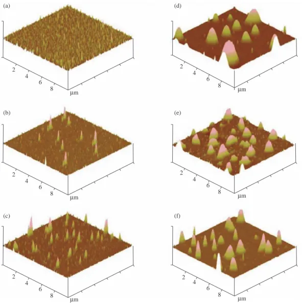
From Fig. 7, the root-mean-square-roughness at p.p, p.1, p.3, p.5, p.9, and p.10 were found to be 1.58, 3.38, 5.38, 16.02, 10.06 and 10.69 nm, respectively. The morphology gradually changed from irregular and uneven clusters near the RF coil to homogenous and smooth films further away from the coil regions (with low RF-fluxes). PPP-OFT films deposited at positions far away from the RF coil and close to the monomer inlet showed lower roughness than the films deposited near the high RF-flux regions. Since short circuit problems in OLED devices fre-quently arise from defects or spikes at organic interfaces, the ITO-glass substrates are remotely
positioned away from the RF-flux regions under the plasma polymerizations. This ensures that the ion energies and the concentrations of the layer growth precursors are de-coupled, and the unwanted species in the growing layers are also reduced.
A pulsed (a duty cycle of 0.3) plasma polymeri-zation, using a low average power input of 9 W, was performed on an oxygen-plasma-treated ITO surface to deposit a PPP-OFT film about 30 cm away from the RF coil. Thin PPP-OFT films of various thicknesses, as hole-injection layers, were inserted between the oxygen-plasma-treated ITO electrode and the NPB layer to fabricate OLED devices with im-proved performance.
IV. CONCLUSION
The experimental results, as stated above, re-veal that fluorinated polymer films can maintain the aromatic structures of octafluorotoluene mono-mers at both a lower duty cycle and a remote sub-strate location. In addition, because there were more dangling bonds in the plasma zone, which easily re-acted with octafluorotoluene monomers, PPP-OFT films had different chemical compositions on surfaces and in interiors of thin films. Moreover, PPP-OFT films including high F/C ratios and high CF2 contents of PTFE-like films can be obtained at different positions of a plasma reactor due to various sticking coefficients of octafluorotoluene free radicals. In addition to F/C ratio and roughness, other factors, such as chemical reactions at interfaces, have to be taken into account to produce thin films for use in EL devices. Further studies to interpret the ex-perimental results and to enhance EL device perfor-mance are under way.
ACKNOWLEDGMENTS
The authors would like to express thanks for the financial and experimental support from Chung-Shan Institute of Science and Technology (in Taiwan).
1080 Journal of the Chinese Institute of Engineers, Vol. 33, No. 7 (2010)
REFERENCES
Chan, K. S., Yang, M. R., and Hsu, S. T., 1999, “Fab-rication and Characteristics of Fluorine Contained Films by Plasma Polymerization of Octafluoro-toluene,” Materials Chemistry and Physic, No. 61, pp. 214-218.
Gao, D. Q., Chan, M. Y., Tong, S. W., Wong, F. L., Lai, S. L., Lee, C. S., and Lee, S. T., 2004, “Ap-plication of an Evaporable Fluoro-Molecule as an Anode Buffer Layer in Organic Electrolumines-cent Devices,” Chemical Physics Letters, Vol. 399, No. 4-6, pp. 337-341.
Gao, Y., Wang, L., Zhang, D., Duan, L., Dong, G., and Qiu, Y., 2003, “Bright Single-Active Layer Small-Molecular Organic Light-Emitting Diodes with a Polytetrafluoroethylene Barrier,” Applied
Physics Letters, Vol. 82, No. 2, pp. 155-157.
Fig. 7 AFM images (3D) on the surfaces of ITO/PPP-OFT films over an area of 10 µm × 10 µm show the root-mean-square roughness at
a) p.p, b) p.1, c) p.3, d) p.5, e) p.9, and f) p.10 were found to be 1.58, 3.38, 5.38, 16.02, 10.06 and 10.69 nm, respectively 2 4 6 8 µm 2 4 6 8 µm 2 4 6 8 µm 2 4 6 8 µm 2 4 6 8 µm 2 4 6 8 µm (a) (d) (b) (e) (c) (f)
Hung, L. S., Zheng, L. R., and Mason, M. G., 2001, “Anode Modification in Organic Light-Emitting Diodes by Low-Frequency Plasma Polymerization on CHF3,” Applied Physics Letters, Vol. 78, No. 5, pp. 673-675.
Kim, Y., Kim, K. J., and Lee, Y., 2009, “Surface Analysis of Fluorine-Containing Thin Films Fab-ricated by Various Plasma Polymerization Methods,” Surface and Coatings Technology, Vol. 203, No. 20-21, pp. 3129-3135.
Kinmond, E. J., Coulson, S. R., Badyal, J. P. S., Brewer, S. A., and Willis, C., 2005, “High Struc-tural Retention during Pulsed Plasma Polymer-ization of 1H,1H,2H-Perfluorododecene: an NMR and TOF-SIMS Study,” Polymer,Vol. 46, No. 18, pp. 6829-6835.
Tamirisa, P. A., Liddel, K. C., Pedrow, P. D., and Osman, M. A., 2004, “Pulsed-Plasma-Polymerized
Aniline Thin Films,” Journal of Applied Polymer
Science, Vol. 93, No. 3, pp. 1317-1325.
Tong, S. W., Lee, C. S., Lifshitz, Y., Gao, D. Q., and Lee, S. T., “Conducting Fluorocarbon Coating for Organic Light-Emitting Diodes,” Applied
Phys-ics Letters, Vol. 78, No. 20, pp. 4032-4034.
Van Slyke, S. A., Chen, C. H., and Tang, C. W., 1996,
“Organic Electroluminescent Devices with Im-proved Stability,” Applied Physics Letters, Vol. 69, No. 15, pp. 2160-2162.
Manuscript Received: Jul. 21, 2009 Revision Received: Aug. 06, 2009 and Accepted: Sep. 06, 2009