Research Article
Indium-Nitrogen Codoped Zinc Oxide Thin Film Deposited by
Ultrasonic Spray Pyrolysis on n-(111) Si Substrate: The Effect of
Film Thickness
Cheng-Chang Yu,
1Wen-How Lan,
2and Kai-Feng Huang
11Department of Electrophysics, National Chiao Tung University, Hsinchu 300, Taiwan
2Department of Electrical Engineering, National University of Kaohsiung, Kaohsiung 811, Taiwan
Correspondence should be addressed to Wen-How Lan; wwhlan@gmail.com
Received 2 October 2013; Revised 27 November 2013; Accepted 12 December 2013; Published 13 February 2014 Academic Editor: Ajay Soni
Copyright © 2014 Cheng-Chang Yu et al. This is an open access article distributed under the Creative Commons Attribution License, which permits unrestricted use, distribution, and reproduction in any medium, provided the original work is properly cited.
Indium-nitrogen codoped zinc oxide (INZO) thin films were fabricated by spray pyrolysis deposition technique on n-(111) Si
substrate with different film thicknesses at 450∘C using a precursor containing zinc acetate, ammonium acetate, and indium
nitrate with 1 : 3 : 0.05 at.% concentration. The morphology and structure studies were carried out by scanning electron microscopy (SEM) and X-ray diffraction (XRD). The grain size of the films increased when increasing the film thickness. From XRD spectra, polycrystalline ZnO structure can be observed and the preferred orientation behavior varied from (002) to (101) as the film thickness increased. The concentration and mobility were investigated by Hall effect measurement. the p-type films with a hole mobility
around 3 cm2V−1s−1and hole concentration around3 × 1019cm−3can be achieved with film thickness less than 385 nm. The n-type
conduction with concentration1 × 1020cm−3is observed for film with thickness 1089 nm. The defect states were characterized by
photoluminescence. With temperature-dependent conductivity analysis, acceptor state with activation energy 0.139 eV dominate the p type conduction for thin INZO film. And the Zn-related shallow donors with activation energy 0.029 eV dominate the n-type conduction for the thick INZO film.
1. Introduction
In recent years, the zinc oxide (ZnO) based materials have attracted much attention. Lots of devices have been studied in many fields [1–6]. For unintentionally doped ZnO, it is usu-ally an n-type semiconductor with carriers from the donor levels associated with oxygen vacancies and/or interstitial zinc atoms [7,8]. High quality n-type ZnO with Al, Ga, and In has been reported [9–11]. To achieve p-type ZnO, a popular method is using nitrogen doping as shallow acceptor [12] although the stability of nitrogen in ZnO is a topic [13]. In the meantime, the nitrogen codoping with certain reactive elements such as Al, Ga, and In was proposed to enhance the solubility and stability of nitrogen in ZnO [14–16]. As the nitrogen chemical states varied with the added In element [16], stable and high p-type concentration can be achieved from the In-N codoped ZnO film. Different deposition meth-ods such as sputtering [17,18], sol-gel spin coating [19], and
ultrasonic spray pyrolysis (USP) [16,20] were applied. Some studies of the In-N codoped ZnO about the electrical and optical properties [16,18, 19], different substrate effect [21], and film postannealing effect [17] were performed. In these studies, all the thickness of the In-N co-doped ZnO was less than 0.5 um, as ZnO film properties show a film thickness-dependent behavior [22–24]. Yet, there is less studies about the thicknesses effects for the In-N codoped ZnO film. In this work, we prepared the In-N codoped ZnO thin films by spray pyrolysis with different film thickness and analyzed their morphology, crystalline, and electrical properties. The photoluminescence and activation energies analysis were applied for understanding the conductivity behaviors.
2. Materials and Methods
The indium and nitrogen co-doped ZnO (INZO) thin film was deposited on n+ (111) Si substrate at 475∘C by spray
Volume 2014, Article ID 861234, 7 pages http://dx.doi.org/10.1155/2014/861234
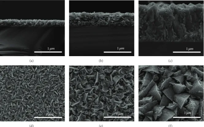
1 𝜇m (a) 1 𝜇m (b) 1 𝜇m (c) 1 𝜇m (d) 1 𝜇m (e) 1 𝜇m (f)
Figure 1: SEM view of cross-section for the ZnO films with different deposited thicknesses: (a) 154 nm, S1, (b) 385 nm, S2, and (c) 1089 nm, S3. The corresponding surface morphologies were shown in (d) S1, (e) S2, and (f) S3, respectively.
pyrolysis [8]. Before deposition, the Si substrate was cleaned by standard cleaning process [25] followed by rinse in HF : H2O = 1 : 20 for 20 s to remove the oxide layer. The INZO film was formed from the pyrolysis of the precursor of zinc acetate, ammonium acetate, and indium (III) chloride with ratio 1 : 3 : 0.05 with different spraying times. The surface morphology and cross-section of the film were studied using scanning electron microscopy (SEM, HITACHI S-4300). The crystalline structure was obtained by X-ray diffraction (XRD, Bruker D8) with Cu K-alpha radiation. The conductivity was obtained by the van der Pauw four-point method (KEITHLEY 2400) and carrier concentration and mobility were obtained by Hall measurement at the magnetic field strength 0.42 T. The temperature-dependent conductivity properties were characterized with a temperature-controlled stage. The photoluminescence (PL) measurement was carried on MiniPL5.0 system (PHOTON SYSTEMS Inc.) with NeCu (248 nm) pulse laser. The depth profile was obtained by secondary ion mass spectrometry (SIMS, Cameca IMS-6f) from MA-tek Inc.
3. Results and Discussion
The morphologies of these INZO films were shown in
Figure 1. The cross-section was shown in (a) sample S1, (b) sample S2, and (c) sample S3. The film thicknesses measured from the cross-sectional images are 154 nm (S1), 385 nm (S2), and 1089 nm (S3), respectively, as listed inTable 1. The corresponding surface morphologies were shown in (d) S1
(e) S2, and (f) S3, respectively. It is clearly shown that the surface morphologies of the INZO films were considerably affected by film thickness. For thin INZO film as shown in
Figure 1(d), the granular structure with some hexagonal plate can be observed. As the film thickness increases by increasing the deposition time, the surface granular structure becomes larger and the cubic-like morphology can be observed in
Figure 1(f).
The X-ray diffraction patterns of the INZO films are shown inFigure 2. There are five peaks distinguished in the figure. All these peaks, as labelled in the figure, can be indexed to ZnO structure.
The three obvious ZnO peaks were indexed as (100), (002), and (101) planes. For thin INZO film (S1), a dominant (002) peak can be observed inFigure 2(a). The (002) peak intensity decreased with increasing film thickness. The film with thickness 1089 nm (S3) showed a primary (101) peak. A relative intensity increasing for (110) peak can be observed also as the film thickness increased. The full-width-half-maximum (FWHM) values of (101) peak were evaluated in Figure 3. The FWHM decreasing with film thickness increasing can be observed. Based on Scherrer’s formula, the averaged grain size𝐷 for the film can be calculated as [26]
𝐷 = 𝛽 cos 𝜃0.94𝜆 , (1)
where𝜃 is the Bragg diffraction angle, 𝜆 is the wavelength of the incident radiation, and𝛽 is FWHM of the diffraction ray. The grain size estimated from the (101) peak in the XRD
(a) (002) (110) (102) (100) (101) (b) (c) In te n si ty (a.u .) 20 30 40 50 60 2𝜃 (deg)
Figure 2: XRD spectra for the ZnO films with different deposited thicknesses: (a) S1, (b) S2, and (c) S3.
0.0 0.2 0.4 0.6 0.8 1.0 1.2 0.20 0.25 0.30 0.35 0.40 20 25 30 35 FWHM (deg) Thickness (𝜇m) D (nm)
Figure 3: The FWHM of the XRD (101) plane and the grain size𝐷.
pattern was shown inFigure 3also. The grain size increases as the film thickness increases. For thick sample S3, the calculated grain size 36.6 nm is quite small than the observed cubic size estimated fromFigure 1(f). As sectional aligned small grain size formed on the substrate/film interface as shown in Figure 1(c). The calculated grain size shows the average effect on the film.
The texture coefficient TC(hkl), which represents the tex-ture of the particular (hkl) plane of a film, was well known as [27] TC(hkl)= Im(hkl) Io(hkl) ÷ 1 𝑁 𝑁 ∑ 1 Im(hkl) Io(hkl), (2) where Im(hkl) and Io(hkl) are the measured and referenced peak intensities in JCPDS of the diffraction peak from the
Table 1: Texture coefficient TC(002)and TC(101)for samples S1 to S3.
Sample Thickness (nm) TC(002) TC(101) S1 154 2.44 0.30 S2 385 2.07 0.52 S3 1089 0.66 1.74 2 4 6 8 0.0 0.2 0.4 0.6 0.8 1.0 1.2 0 1 2 3 (a) n-type (b) p-type (c) 1020 1019 Thickness (𝜇m) C o ncen tra tio n (cm −3) Rsh (× 10 3Ω/ sq .) 𝜇( cm −1 V −1 s −1)
Figure 4: The conduction properties of ZnO thin films with
dif-ferent deposited thicknesses: (a) the sheet resistance𝑅sh, (b) carrier
concentration, and (c) Hall mobility𝜇.
(hkl) plane. The number𝑁 is the total number of reflection peaks. The calculated (002) and (101) texture coefficient val-ues TC(002) and TC(101) were shown in Table 1. For thin INZO sample S1, the TC(002) has the highest value. The main structure is (002) plane. The dominant (002) plane phenomenon can be observed in several thin ZnO films [24,27]. The preferential orientation of c-axis for thin INZO leads to the enhancement of high TC(002)values. As the film thickness increases, the TC(002)value decreases and TC(101) value increases. The preferred texture changed from (002) to (101) with the film thickness increasing. The texture change, which may probably be due to the growth mode variance [24], results in the corresponding surface morphology difference as shown in Figures1(d)–1(f).
The sheet resistance (𝑅sh), concentration, and mobility
(𝜇) for the INZO films with different thickness are shown in Figures4(a),4(b), and4(c), respectively. To verify the stability of the films, these properties were tested again after one month later and the quantity variation less than 12% was observed. The sheet resistance decreases as the film thickness increases. From Hall measurement, p-type conduction was characterized for sample S1 and S2 while the n-type conduc-tion was characterized for sample S3. The p-type concentra-tion around2 × 1019cm−3, which is near the reported In-N codoped ZnO film values [16,19,20], reveals the efficient
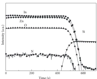
0 200 400 600 In te n si ty (a.u .) Time (s) In Zn O N Si
Figure 5: SIMS depth profile of sample S3.
nitrogen incorporation in ZnO film [21]. For the thickest sample S3, the n-type conduction around1 × 1020cm−3can be observed. Compared with sample S2, an enormous change for sample S3 in carrier density from p-type to n-type would require a large carrier compensation mechanism.
In order to clarify the element composition in this INZO film, SIMS depth profile was carried out on sample S3 as shown inFigure 5. The content of In and N as well as Zn and O remains constant throughout the whole film was observed. No obvious In and N composition variation in the film. As the film morphology and preferential orientation change as the film thickness increases, different chemical states may occur with different thickness and dominate the film conduction.
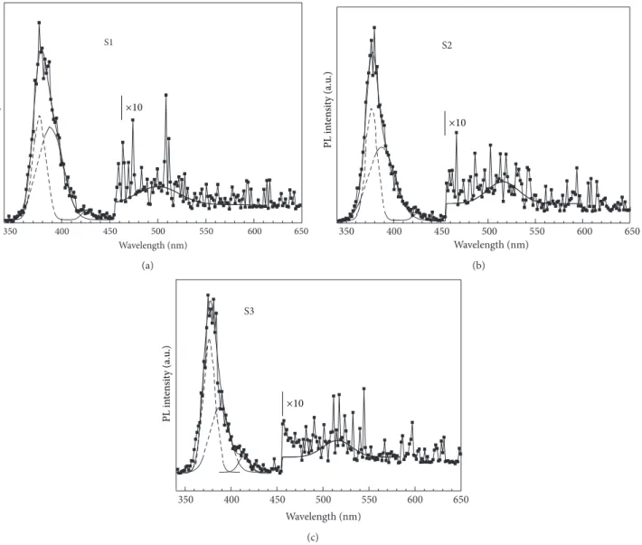
Figure 6shows the room temperature PL spectra of the three samples. For sample S1, as shown inFigure 6(a), a near band edge emission with peak wavelength 376 nm can be observed [28–30]. This broadened emission may split to two peaks after Gaussian fitting process [29]. Dominant peak with wavelength 376 nm (3.30 eV) is attributed to near band edge emission of bound neutral donors (D∘X). Another emission peak with fitted peak wavelength around 388 nm (3.20 eV) can be observed in the figure. This peak, which is near the reported peak at 384 nm, may be attributed to the complex defects and arises from the energy transition between donor-acceptor pairs (DAP) [29–31]. A small peak around 425 nm (2.92 eV) can be observed in the figure. Lots of emissions originating from interstitial zinc-related defects were found in this range (415–470 nm) in the p-type Al-N codoped ZnO film [22]. The emission at 425 nm may be attributed to the transition related interstitial zinc-related defect (Zni).
A visible emission with peak wavelength 500 nm (2.48 eV) can be observed. This peak is attributed to the singly ionized oxygen vacancies[VO+] [29, 31, 32] or zinc
interstitial [33] and can be observed in the p-type N doped ZnO [33].
For sample S2, similar emission peaks can be observed. The increasing of emission intensity ratio of D∘X/DAP can be observed. Besides, broadened emission with peak wavelength around 520 nm (2.38 eV) can be observed. The emission with
Table 2: The activation energies𝐸𝐴for different samples.
Sample Activation energy𝐸𝐴(eV)
S1 0.144 (T = 300 K–350 K)
S2 0.139 (T = 300 K–390 K)
S3 0.029 (T = 300 K–390 K)
peak wavelength 498 nm as seen in sample S1 may be inclosed in this broadened emission band. This green emission which can be observed in many ZnO film [28,29] is attributed to the transition of conduction band to the oxygen antisite state [OZn] [28], radiative optical transition in interstitial oxygen
[Oi] [29], or the zinc vacancy[VZn]-related defect transition
[28,32].
For sample S3, with film thickness increasing, the emis-sion intensity ratio of D∘X/DAP increases more and the fitted bandwidth for DAP decreases. An emission with peak wavelength 415 nm (2.99 eV) can be observed. This emission, which still lies in the spectral range as mentioned (415– 470 nm), was attributed to certain Znidefects [22]. Compare with sample S2, the appearance of the peak reveals that some certain Znidefects were enhanced for thick INZO films. As the ionization energy for this n-type defect Zniis only 50 meV [34], high electron concentration may come from such defect state at room temperature.
For further understanding the carrier conduction mech-anism, temperature-dependent conductivity measurement was carried out for all samples. For the semiconductor film with grain structure, the film conductivity may be affected by the grain size and electronic mean free path [35,36]. To estimate the effect of grain boundary scattering, the mean free path𝑙 for carriers in the film can be calculated as [35]
𝑙 = (2𝑒ℎ) (3𝑛𝜋)1/3𝜇, (3) where 𝑛 and 𝜇 are the carrier concentration and mobility, respectively. The calculated values at room temperature are 17 nm (S1), 22 nm (S2), and 5 nm (S3), respectively. These results all are less than the crystalline grain size𝐷, suggesting that the contribution from the grain boundary scattering mechanism at room temperature can be neglected.
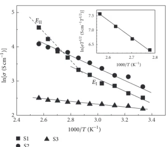
Figure 7shows the conductivity measured with different temperatures for samples S1 to S3. For semiconductor with electrical conductivity dominated by the activation of doping level, the relationship between electrical conductivity𝜎 and the measurement temperature𝑇 is given by [26]
𝜎 = 𝜎0exp(−𝐸𝐴
𝑘𝑇) , (4)
where 𝜎0 is the preexponential factor, 𝑘 is the Boltzmann constant, and𝐸𝐴is the activation energy. The calculated𝐸𝐴 values were listed inTable 2.
For S1, two different regions in different temperature ranges can be observed. This suggests the presence of two different sorts of conduction mechanism in sample S1. Activa-tion energy values for region I (300 K to 350 K) and II (360 to 390 K) were calculate, respectively, from the linear portions.
350 400 450 500 550 600 650 Wavelength (nm) S1 PL in te n si ty (a.u .) ×10 (a) 350 400 450 500 550 600 650 Wavelength (nm) S2 PL in te n si ty (a.u .) ×10 (b) 350 400 450 500 550 600 650 Wavelength (nm) S3 PL in te n si ty (a.u .) ×10 (c)
Figure 6: Room temperature PL spectra for samples (a) S1, (b) S2, and (c) S3. The Gaussian fitting curves at different spectra ranges were shown.
The obtained𝐸𝐴values are 0.144 eV and 0.491 eV, respectively. For region I, this activation energy value is quite near the reported 0.135–0.14 eV for the N-doped ZnO [37, 38] and thus was assigned as the defect complex of O-site N-Zn vacancy(NO-VZn) [39]. The shallow acceptor coming from
this complex takes p-type concentration contribution in region I.
In region II, the obtained active energy value is relatively small compared with the band gap energy of ZnO. Besides, the activation energy calculated from two adjacent points for S1 in region II increases with temperature. This behavior and energy value, which have been observed for other ZnO based films [26], were corresponding to the grain boundary related scattering. With temperature increasing, the conductivity increases as the increasing of carrier concentration. For S1, the conductivity enhancement of 2.4 times can be observed as the temperature increases from room temperature to 87∘C (1000/𝑇 = 2.78 K−1). If the concentration increases 2.4 times
also with a little mobility drop, the mean free path at 87∘C is
then estimated to be 26 nm. In this case, the mean free path of carriers in sample S1 in region II is larger than the grain size 𝐷; the grain boundary related scattering cannot be neglected. In this case, the conductivity𝜎 controlled by grain boundary can be described as [40,41]
𝜎 = 𝑞2𝑁𝐷
√2𝜋𝑚∗𝑘𝑇exp(−
𝐸𝐵
𝑘𝑇) , (5)
where𝑁 is the carrier concentration, 𝐷 is the grain size, 𝑚∗ is the effective mass, and𝐸𝐵is the mean barrier height across the grain boundary. The inset inFigure 7shows the plot of ln(𝜎𝑇1/2) versus 1000/𝑇 for S1 in region II. The barrier height
𝐸𝐵 of the film was found to be 0.51 eV. The conductivity for S1 in temperature range II (360 K–390 K) is controlled by the grain boundaries. The disordered grain boundaries with trapping state will capture carriers. The conductivity thus is controlled by the transition ability for carriers passing
2.4 2.6 2.8 3.0 3.2 3.4 2 3 4 5 2.6 2.7 2.8 6.5 7.0 7.5 1000/T (K−1) 1000/T (K−1) S1 S2 S3 ln[ 𝜎 (S cm −1)] EI EII In [𝜎T 1/ 2(Sc m −1T 1/ 2)]
Figure 7: Conductivity measured at different temperatures for the ZnO films with different deposited thicknesses.
through the barrier and the conduction mechanism is grain boundary scattering.
For sample S2, a linear relation can be observed in
Figure 7. The extracted activation energy by (4) is 0.139 eV. This value, which is near the previous 0.144 eV, reveals the same conduction mechanism for S2 and S1 in region I, which is dominant by the acceptor complex of NO-VZn.
For the thickest sample S3, a linear relation can be observed inFigure 7also. The extracted activation energy by (3) is 0.029 eV. There is no nitrogen-related state associated with such low activation energy [37–39]. This activation value may correspond to the origin donor level for the indium doped ZnO (0.026 eV) [26] or the interstitial Zni-related complex (0.031 eV) [40]. This shallow donor level, which caused the measured n-type conduction also, dominates the conduction mechanism for the thickest sample S3.
For thick INZO film, the grain size becomes bigger. The effect of hole accumulation in Si substrate interface [42] reduces with the increasing of film thickness. Besides, effect of grain boundary becomes less and the preferential orientation changes also with the increasing of film thickness. The p-type conduction enhanced by grain boundary related states becomes less [42,43]. Both reduce the acceptor concentration and the shallow donor state corresponding to the interstitial Zni-related complex which has dominant effect on the con-duction mechanism for this thick INZO film.
4. Conclusion
In conclusion, INZO thin films were prepared by spray pyrol-ysis, and the effects of film thickness on structure and surface morphology were studied. The thin INZO films showed preferential orientation along the (002) plane with tiny flake morphology. For INZO film with thickness 1089 nm, the preferential orientation was shifted to (101) plane with cubic-like morphology. The conduction type shows p-type for thin film and changes to n-type for the thick film after
the Hall measurement. From the activation analysis coming from the temperature-dependent conductivity measurement, the nitrogen-related acceptor state and the grain boundary scattering dominate the p-type conduction for thin film. The change from p-type to n-type conduction for thick INZO film was characterized by the photoluminescence and activation energy analysis as the appearance of Zn-related shallow donors.
Conflict of Interests
The authors declare that there is no conflict of interests regarding the publication of this paper.
References
[1] J. H¨upkes, B. Rech, O. Kluth et al., “Surface textured MF-sput-tered ZnO films for microcrystalline silicon-based thin-film solar cells,” Solar Energy Materials & Solar Cells, vol. 90, no. 18-19, pp. 3054–3060, 2006.
[2] W.-C. Shih and R.-C. Huang, “Fabrication of high frequency ZnO thin film SAW devices on silicon substrate with a dia-mond-like carbon buffer layer using RF magnetron sputtering,”
Vacuum, vol. 83, no. 3, pp. 675–678, 2008.
[3] S. K. Jha, O. Kutsay, I. Bello, and S. T. Lee, “ZnO nanorod based low turn-on voltage LEDs with wide electroluminescence spec-tra,” Journal of Luminescence, vol. 133, pp. 222–225, 2013. [4] H. S. Al-Salman and M. J. Abdullah, “Effect of Co-doping on the
structure and optical properties of ZnO nanostructure prepared by RF-magnetron sputtering,” Superlattices and Microstructures, vol. 60, pp. 349–357, 2013.
[5] L. Luo, L. Gong, Y. F. Liu et al., “Enhanced ultraviolet lasing from europium-doped zinc oxide nanocrystals,” Optical Materials, vol. 32, no. 9, pp. 1066–1070, 2010.
[6] G. Z. Xing, D. D. Wang, B. Yao, A. Q. L. F. Nien, and Y. S. Yan, “Structural characteristics, low threshold ultraviolet lasing and ultrafast carrier dynamics in high crystalline ZnO nanowire arrays,” Chemical Physics Letters, vol. 515, pp. 132–136, 2011. [7] J. C. Simpson and J. F. Cordaro, “Characterization of deep levels
in zinc oxide,” Journal of Applied Physics, vol. 63, no. 5, pp. 1781– 1783, 1988.
[8] C. C. Yu, Y. T. Hsu, S. Y. Lee et al., “Effects of doping ratio and thermal annealing on structural and electrical properties of boron-doped ZnO thin films by spray pyrolysis,” Japanese
Jour-nal of Applied Physics, vol. 52, Article ID 065502, 5 pages, 2013.
[9] P. Nunes, E. Fortunato, P. Tonello, F. Braz Fernandes, P. Vilar-inho, and R. Martins, “Effect of different dopant elements on the properties of ZnO thin films,” Vacuum, vol. 64, no. 3-4, pp. 281–285, 2002.
[10] Y. Morinaga, K. Sakuragi, N. Fujimura, and T. Ito, “Effect of Ce doping on the growth of ZnO thin films,” Journal of Crystal
Growth, vol. 174, no. 1–4, pp. 691–695, 1997.
[11] A. Tiburcio-Silver, J. C. Joubert, and M. Labeau, “´Etudes sur la croissance, la structure et la composition de couches minces de ZnO et ZnO dop´e a l’indium, obtenues par proc´ed´e pyrosol,”
Thin Solid Films, vol. 197, no. 1-2, pp. 195–214, 1991.
[12] A. Kobayashi, O. G. Sankey, and J. D. Dow, “Deep energy levels of defects in the wurtzite semiconductors AIN, CdS, CdSe, ZnS, and ZnO,” Physical Review B, vol. 28, pp. 946–951, 1983.
[13] X. Chen, Z. Zhang, B. Yao et al., “Effect of compressive stress on stability of N-doped p-type ZnO,” Applied Physics Letters, vol. 99, no. 9, Article ID 091908, 3 pages, 2011.
[14] T. Yamamoto and H. Katayama-Yoshida, “Physics and control of valence states in ZnO by codoping method,” Physica B, vol. 302-303, pp. 155–162, 2001.
[15] M. Joseph, H. Tabata, H. Saeki, K. Ueda, and T. Kawai, “Fab-rication of the low-resistive p-type ZnO by codoping method,”
Physica B, vol. 302-303, pp. 140–148, 2001.
[16] J. M. Bian, X. M. Li, X. D. Gao, W. D. Yu, and L. D. Chen, “Depo-sition and electrical properties of N-In codoped p-type ZnO films by ultrasonic spray pyrolysis,” Applied Physics Letters, vol. 84, no. 4, pp. 541–543, 2004.
[17] N. Yuan, L. Fan, J. Li, and X. Wang, “Post-annealing influence on properties of N-In codoped ZnO thin films prepared by ion beam enhanced deposition method,” Applied Surface Science, vol. 253, no. 11, pp. 4990–4993, 2007.
[18] N. Yuan, J. Li, L. Fan, X. Wang, and Y. Zhou, “Structure, elec-trical and optical properties of N-In codoped ZnO thin films prepared by ion-beam enhanced deposition method,” Journal
of Crystal Growth, vol. 290, no. 1, pp. 156–160, 2006.
[19] Y. Cao, L. Miao, S. Tanemura, M. Tanemura, Y. Kuno, and Y. Hayashi, “Low resistivity p-ZnO films fabricated by sol-gel spin coating,” Applied Physics Letters, vol. 88, no. 25, Article ID 251116, 3 pages, 2006.
[20] J. Bian, X. Li, L. Chen, and Q. Yao, “Properties of undoped n-type ZnO film and N-In codoped p-n-type ZnO film deposited by ultrasonic spray pyrolysis,” Chemical Physics Letters, vol. 393, no. 1–3, pp. 256–259, 2004.
[21] L. L. Chen, J. G. Lu, Z. Z. Ye et al., “p-type behavior in In-N codoped ZnO thin films,” Applied Physics Letters, vol. 87, Article ID 252106, 3 pages, 2005.
[22] A. Zhong, J. Tana, H. Huanga, S. Chena, M. Wanga, and S. Xua, “Thickness effect on the evolution of morphology and optical properties of ZnO films,” Applied Surface Science, vol. 257, no. 9, pp. 4051–4055, 2011.
[23] Y. H. Kang, J.-H. Choi, T. I. Lee, W. Lee, and J.-M. Myoung, “Thickness dependence of the resistive switching behavior of nonvolatile memory device structures based on undoped ZnO films,” Solid State Communications, vol. 151, no. 23, pp. 1739– 1742, 2011.
[24] L. Xu, X. Li, Y. Chen, and F. Xu, “Structural and optical proper-ties of ZnO thin films prepared by sol-gel method with different thickness,” Applied Surface Science, vol. 257, no. 9, pp. 4031–4037, 2011.
[25] W. Kern, “The evolution of silicon wafer cleaning technology,”
Journal of the Electrochemical Society, vol. 137, no. 6, pp. 1887–
1892, 1990.
[26] M. Benhaliliba, C. E. Benouis, M. S. Aida, F. Yakuphanoglu, and A. Sanchez Juarez, “Indium and aluminium-doped ZnO thin films deposited onto FTO substrates: nanostructure, optical, photoluminescence and electrical properties,” Journal of Sol-Gel
Science and Technology, vol. 55, no. 3, pp. 335–342, 2010.
[27] S. Ilican, Y. Caglar, M. Caglar, and F. Yakuphanoglu, “Electrical conductivity, optical and structural properties of indium-doped ZnO nanofiber thin film deposited by spray pyrolysis method,”
Physica E, vol. 35, no. 1, pp. 131–138, 2006.
[28] A. S. Gadallah and M. M. E. Nahass, “Structural, optical con-stants and photoluminescence of ZnO thin films grown by Sol-Gel spin coating,” Advances in Condensed Matter Physics, vol. 2013, Article ID 234546, 11 pages, 2013.
[29] A. C. Rastogi, S. B. Desu, P. Bhattacharya, and R. S. Katiyar, “Effect of strain gradation on luminescence and electronic prop-erties of pulsed laser deposited zinc oxide thin films,” Journal of
Electroceramics, vol. 13, no. 1–3, pp. 345–352, 2004.
[30] C. V. Manzano, D. Alegre, O. C. Calero, B. Alen, and M. S. M. Gonzalez, “Synthesis and luminescence properties of electrode-posited ZnO films,” Journal of Applied Physics, vol. 110, Article ID 043538, 3 pages, 2011.
[31] J. C. Fan, K. M. Sreekanth, Z. Xie, S. L. Chang, and K. V. Rao, “p-type ZnO materials: theory, growth, properties and devices,”
Progress in Materials Science, vol. 58, no. 6, pp. 847–985, 2013.
[32] S. Golshahi, S. M. Rozati, R. Martins, and E. Fortunato, “p-type ZnO thin film deposited by spray pyrolysis technique: the effect of solution concentration,” Thin Solid Films, vol. 518, no. 4, pp. 1149–1152, 2009.
[33] J. C. Sun, H. W. Liang, J. Z. Zhao et al., “Ultraviolet electrolu-minescence from n-ZnO:Ga/p-ZnO:N homojunction device on sapphire substrate with p-type ZnO:N layer formed by
anneal-ing in N2O plasma ambient,” Chemical Physics Letters, vol. 460,
no. 4–6, pp. 548–551, 2008.
[34] L. Schmidt-Mende and J. L. MacManus-Driscoll, “ZnO—nano-structures, defects, and devices,” Materials Today, vol. 10, no. 5, pp. 40–48, 2007.
[35] M. Chen, Z. L. Pei, X. Wang et al., “Intrinsic limit of electrical properties of transparent conductive oxide films,” Journal of
Physics D, vol. 33, no. 20, pp. 2538–2541, 2000.
[36] L. L. Chen, Z. Z. Ye, J. G. Lu et al., “Co-doping effects and electrical transport in In-N doped zinc oxide,” Chemical Physics
Letters, vol. 432, no. 1–3, pp. 352–355, 2006.
[37] D. C. Look, “Electrical and optical properties of p-type ZnO,”
Semiconductor Science and Technology, vol. 20, no. 4, pp. 55–61,
2005.
[38] H. B. Ye, J. F. Kong, W. Z. Shen, J. L. Zhao, and X. M. Li, “Tem-perature-dependent photoluminescence of undoped, N-doped and N-In codoped ZnO thin films,” Journal of Physics D, vol. 40, no. 18, pp. 5588–5591, 2007.
[39] L. Liu, J. Xu, D. Wang et al., “p-type conductivity in N-doped
ZnO: the role of the NZn-VOcomplex,” Physical Review Letters,
vol. 108, no. 21, Article ID 215501, 5 pages, 2012.
[40] ¨U. ¨Ozg¨ur, Y. I. Alivov, C. Liu et al., “A comprehensive review of
ZnO materials and devices,” Journal of Applied Physics, vol. 98, Article ID 041301, 4 pages, 2005.
[41] N. C. C. Lu, L. Gerzberg, C. Y. Lu, and J. D. Meindl, “Modeling and optimization of monolithic polycrystalline silicon resis-tors,” IEEE Transactions on Electron Devices, vol. 28, no. 7, pp. 818–830, 1981.
[42] J. L. Zhao, X. M. Li, A. Krtschil et al., “Ultraviolet and visible
electroluminescence from n-ZnO/SiO𝑥/(n,p)-Si
heterostruc-tured light-emitting diodes,” Applied Physics Letters, vol. 90, Article ID 062118, 3 pages, 2007.
[43] B. Wang, J. Min, Y. Zhao, W. Sang, and C. W. Gao, “The grain boundary related p-type conductivity in ZnO films prepared by ultrasonic spray pyrolysis,” Applied Physics Letters, vol. 94, Article ID 192101, 3 pages, 2009.
Submit your manuscripts at
http://www.hindawi.com
Scientifica
Hindawi Publishing Corporation
http://www.hindawi.com Volume 2014
Corrosion
Hindawi Publishing Corporationhttp://www.hindawi.com Volume 2014
Hindawi Publishing Corporation
http://www.hindawi.com Volume 2014
Polymer Science
International Journal ofHindawi Publishing Corporation
http://www.hindawi.com Volume 2014
Ceramics
Journal ofHindawi Publishing Corporation
http://www.hindawi.com Volume 2014
Composites
Nanoparticles
Journal of Hindawi Publishing Corporationhttp://www.hindawi.com Volume 2014
Hindawi Publishing Corporation
http://www.hindawi.com Volume 2014
International Journal of
Biomaterials
Hindawi Publishing Corporation
http://www.hindawi.com Volume 2014
Nanoscience
Journal ofTextiles
Hindawi Publishing Corporation
http://www.hindawi.com Volume 2014
Journal of
Nanotechnology
Hindawi Publishing Corporation
http://www.hindawi.com Volume 2014
Hindawi Publishing Corporation
http://www.hindawi.com Volume 2014
Crystallography
Journal ofThe Scientific
World Journal
Hindawi Publishing Corporation
http://www.hindawi.com Volume 2014
Hindawi Publishing Corporation
http://www.hindawi.com Volume 2014
Coatings
Journal ofAdvances in
Materials Science and Engineering
Hindawi Publishing Corporation
http://www.hindawi.com Volume 2014
Research
Hindawi Publishing Corporation
http://www.hindawi.com Volume 2014
Hindawi Publishing Corporation
http://www.hindawi.com Volume 2014
Metallurgy
Journal of Hindawi Publishing Corporationhttp://www.hindawi.com Volume 2014
Research International
Hindawi Publishing Corporation
http://www.hindawi.com Volume 2014
Materials
Journal ofN
a
no
ma
te
ria
ls
Hindawi Publishing Corporation
http://www.hindawi.com Volume 2014
Journal of