國 立 交 通 大 學
電子工程學系 電子研究所
碩士論文
奈米快閃記憶體之特性與研究
Characteristics and Investigation of Nano
Flash Memory
研 究 生:謝智仁 Chih-Ren Hsieh
指導教授:羅正忠 博士 Dr.Jen-Chung Lou
葉清發 博士 Dr.Ching-Fa Yeh
奈米快閃記憶體之特性與研究
Characteristics and Investigation of Nano
Flash Memory
研 究 生:謝智仁
Student:Chih-Ren Hsieh
指導教授:羅正忠 博士 Advisor:Dr.Jen-Chung Lou
葉清發 博士
Advisor:
Dr.Ching-Fa Yeh
國 立 交 通 大 學
電子工程學系 電子研究所
碩 士 論 文
A Thesis
Submitted to
Department of Electronics Engineering & Institute of Electronics
College of Electrical and Computer Engineering
National Chiao Tung University
In Partial Fulfillment of the Requirements
For the Degree of Master
In
Electronic Engineering
June 2007
Hsinchu, Taiwan, Republic of China
摘要
奈米快閃記憶體之
特性與研究
研究生:謝智仁 指導教授:羅正忠 博士 葉清發 博士 國立交通大學 電子工程學系 電子研究所 摘要 傳統的非揮發性記憶體是利用複晶矽浮停閘(floating gate)做為載子儲存的 單元,當浮停閘儲存由通道注入的電子之後,元件的起始電壓就會發生改變,利用 起始電壓的差異作為記憶體0 和1 邏輯的定義。隨著系統晶片(SOC)的發展,持 續降低互補式金氧半(CMOS)場效電晶體元件中的閘極判電層及非揮發性記憶 體(non-volatile memories)中的複晶矽層間介電層(inter-poly dielectric)厚度以提 高元件密度及降低操作電壓變得十分重要。但當氧化層厚度小於7奈米時,原本 儲存於複晶矽浮停閘內的電荷,很容易因為氧化層中的缺陷,形成漏電流路徑, 一旦穿隧氧化層(tunnel oxide)出現漏電路徑,儲存的電荷就會全部流失,記憶 體就會失效。於是,以奈米點(nano dot)為儲存介質的新式NVM結構被提出以作 為離散式儲存方式的記憶體,以順應尺寸微縮以及維持好的儲存能力等特性。在 本篇論文中,我們利用金屬材料來製作出以奈米點或薄膜做為補陷電子媒介的記利用半導體或金屬奈米點作為電荷儲存的單元,在元件的反覆操作下,即使穿 隧氧化層產生缺陷或漏電路徑,所損失掉的儲存電子,僅是單一奈米點的電子漏 失,對整體元件特性的影響並不明顯。因此,穿隧氧化層的厚度得以縮減,使得操 作速度提升,元件積集度增加,元件可操作的次數(endurance)以及保存時間 (retention)也同時得到改善,當電子儲存在奈米點時,由於庫倫阻絕(Coulomb blockade)效應,儲存的電子會限制後續電子的注入。奈米點的庫倫阻絕效應使得 記憶體元件的儲存及操作更加的穩健。 首先,本研究提出於穿隧氧化層上利用雙電子槍蒸鍍系統將金屬材料-鉑(Pt) 沉積在試片上,之後覆蓋上SiO2做為控制氧化層,再經由高溫退火使之形成奈米 點,以製造出奈米點結構記憶體。藉由這種方法我們可以得到具有低外加偏壓、 大記憶窗口、快速寫入/抹除速度、高穩定性的非揮發性記憶體。同時,我們也 預測可以用元件做一個單元儲存兩個位元的操作方式。因此,我們認為,利用Pt 作為奈米點結構記憶體的材料是很有潛力且備受期待的。
ABSTRACT
Characteristics and Investigation of Nano
Flash Memory
Student:Chih-Ren Hsieh Advisor:Dr.Jen-Chung Lou Dr.Ching-Fa Yeh Department of Electronics Engineering &Institute of Electronics
College of Electrical and Computer Engineering National Chiao-Tung University
Abstract
In a conventional nonvolatile memory, charge is stored in a polysilicon floating gate (FG) surrounded by dielectrics. The scaling limitation stems from the requirement of very thin tunnel oxide layer. For FG, once the tunnel oxide develops a leakage path under repeated write/erase operation, all the stored charge will be lost. For the system-on-chip (SOC) application, a continuously scaling of the gate dielectrics for complementary metal oxide semiconductor (CMOS) and inter-poly dielectrics (IPDs) for electrically-erasable programmable read-only-memory (EEPROM) and stacked-gate flash memory is needed to obtain high density and low operation voltage. But when oxide thickness is less than 7nm, the charge stored in the floating gate forming leakage path easily due to defects in the oxide, thus induces data error. To overcome the limits of the conventional FG structure, other kinds of nonvolatile memories such as SONOS and nanocrystal memories which stored
electrons in discrete traps are mostly mentioned, hence several characteristics such as scaling down and good storage maintenance can be reached. In this thesis, we successfully fabricated nanocrystral memory device by using metal materials. Nanocrystal charge storage offers several advantages, the main one being the potential to use thinner tunnel oxide without sacrificing nonvolatile. This is a quite attractive proposition since reducing the tunnel oxide thickness is a key to lowering operating voltages and/or increasing operating speeds. The improved scalability results not only from the distributed nature of the charge storage, which makes the storage more robust and fault-tolerant, but also from the beneficial effects of Coulomb blockade. A local leaky path will not cause a fatal loss of information for the nanocrystal nonvolatile memory device. Also, the nanocrystal memory device can maintain good retention characteristics and lower the power consumption.
First, a Platinum metal material layer was deposited on the oxide by Dual E-gun Evaporation System with Pt targets, then cap with SiO2. After that, the wafer was
subjected to RTA treatment in N2 ambient at some temperature and time. When the
film is RTA treated to provide enough energy and surface mobility, the thin Platinum material will self-assemble in to nano dot. By using the method, we obtain nonvolatile memory devices with excellent characteristics:low applied voltages, large memory window, high program/erase speed, fine endurance. And, we forecast that can use these devices in 2-bit operation . Consequently, we consider, it is potential material as nanocrystal memory devices by using Platinum.
誌謝
在二年的幸苦耕耘努力之下,此篇碩士論文才能順利完成,心中
有太多的情感要疏發也有許多的人需要我一一的去感謝,感謝他們在
這兩年來給我的指導,讓我在茫茫的未來點亮了一盞明亮的燈。首
先,要感謝我的指導教授葉清發博士和羅正忠博士,在二年的指導讓
我學習到很多做研究的方法以及為人處世的方法。其次要感謝實驗室
的學長們,柏村學長的關懷與指導讓我在論文實驗的過程有了相當大
的依靠也積極的幫實驗室尋找經費,永裕學長也在百忙之下抽空時常
的為我們的實驗進度上的困惑解答,還有伯翰學長、國源學長、愛玉
學長教導量測的方法以及做實驗的技巧。再者,要感謝我女朋友雅伶
在背後默默支持與鼓勵才讓我有足夠的力量和精神去衝刺我的實
驗,也感謝很愛碎碎唸的德安、愛逞強的王董、一點都不像老師的正
凱、努力創戰隊的大峰、做事猶豫不決的小天、疼老婆的建宏、時常
偷偷出現的大勒哥、天天都沉醉在愛的世界裡的阿龍、為實驗室默默
付出的學弟幸福、一直被打屁股的土豆、把女朋友偷偷起來的元愷、
家教上不完的晨修、東風籃球客串交大電子魔獸先生的嘉宏、愈來愈
奸詐狡滑的佳樺,以及奈米中心倪月珍小姐都是陪伴我度過碩士兩年
來的最佳同伴。最後要感謝我的爸爸謝明舜、媽媽林素月、大哥謝育
佑、二哥謝育興、小妹謝育儒在這二年來的支持。有很多話要說,非
常多的話想說,但耐何千言萬語也都表達不了我內心的澎派和我心中
Contents
Abstract(Chinese)---I
Abstract(English)--- III
Acknowledgment (Chinese)---V
Content---VII
Table Captions--- IX
Figure Captions---X
Chapter.1 Introduction of Non-Volatile Memory
1.1 General Background--- 1
1.2 Motivation--- 7
1.3 Organization of This Thesis---8
Chapter.2 Basic principles of nonvolatile memory
2.1 Introduction---132.2 Program/Erase operation mechanisms --- 14
2.3 Nonvolatile Memory Device reliability ---17
2.4 Summary---19
Chapter.3 Experimental Process and discussion of results
3.1 Introduction---243.2 Experimental ---25 3.3 Results and discussions ---28 3.4 Summary---31
Chapter.4 Conclusion and suggestion for future work
4.1 Conclusion--- 57 4.2 Suggestion of Future Work--- 57
Table Captions
Chapter1
Table 1.1 Performance comparison between volatile memory (DRAM & SRAM) and nonvolatile memory (Flash, FRAM, and PCM) device. Flash memory exhibits the best performance except the disadvantages of high programming voltage and slow program/erase speed.
Chapter3
Figure Captions
Chapter1
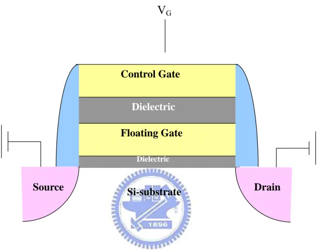
Fig1-1 Schematic cross section of the conventional floating gate nonvolatile memory device. Continuous poly-Si floating gate is used as the charge storage element.
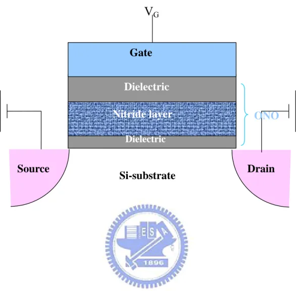
Fig1-2 Schematic cross section of the SONOS nonvolatile memory device. The nitride layer is used as the charge-trapping element.
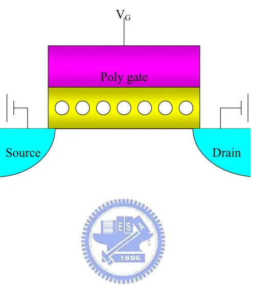
Fig1-3 The structure of the nanocrystal nonvolatile memory device. The semiconductor nanocrystals or metal nano-dots are used as the charge storage element instead of the continuous poly-Si floating gate.
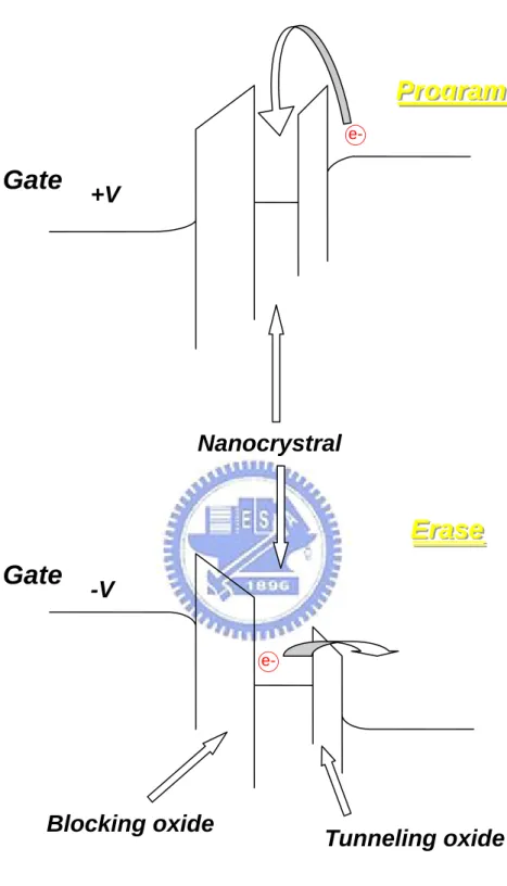
Fig1-4 The energy band diagrams of the write/erase operation for a nanocrystal NVSM device.
Chapter2
Fig2-1 The diagram of channel hot electrons injection (CHEI) Fig2-2 Energy-band representation for explaining FN tunneling Fig2-3 The diagram of band to band hot electron injection Fig2-4 The diagram of band to band hot hole injection
Chapter3
Fig3-1 (a)Schematic cross section of the Pt Nanocrysal capacitor. (b) Process flows for fabricating various Pt Nanocrysal capacitors
Fig3-2 (a)Schematic cross section of the Pt Nanocrysal Device. (b) Process flows for fabricating various Pt Nanocrysal Device.
Fig3-3 The construction of measurement system
Fig3-4 SIMS profile of nitrogen distribution of 25Å oxynitride.
Fig3-5 (a) The C-V hysteresis of the capacitor with anneal 800℃ 3min in N2 process after bidirectional sweeps.(b) The leakage current of the capacitor with anneal 800℃ 3min in N2 process(c) Program characteristics with different programming condition.(d) Erase characteristics with different programming condition(e) Endurance characteristics with anneal 800℃ 3min in N2 of the Pt nanocrystal
Fig3-6 (a) The C-V hysteresis of the capacitor with anneal 800℃ 5min in N2 process after bidirectional sweeps.(b) The leakage current of the capacitor with anneal 800℃ 5min in N2 process.(c)Program characteristics with different programming condition.(d) Erase characteristics with different programming condition(e) Endurance characteristics with anneal 800℃ 5min in N2 of the Pt nanocrystal
Fig3-7 (a)The C-V hysteresis of the capacitor with anneal 800℃ 3min in O2 process
after bidirectional sweeps.(b) The leakage current of the capacitor with anneal 800℃ 3min in O2 process
Fig3-7 (c)Program characteristics with different programming condition.(d) Erase characteristics with different programming condition(e) Endurance characteristics with anneal 800℃ 3min in O2 of the Pt nanocrystal
Fig3-8 (a)The C-V hysteresis of the capacitor with anneal 800℃ 5min in O2 process
after bidirectional sweeps.(b) The leakage current of the capacitor with anneal 800℃ 5min in O2 process. (c) Program characteristics with different
programming condition.(d) Erase characteristics with different programming condition (e)Endurance characteristics with anneal 800℃ 5min in O2 of the
Pt nanocrystal
Fig3-9 Id-Vg cureve of oxide Pt nanocrystal memory. A memory window about 0.6V
can achieved with programmed Vg=Vd=14V 1S and erased Vg=-8V Vd=8V
1S operation
Fig3-10 Id-Vg cureve of oxyenitride Pt nanocrystal memory A memory window about
0.6V can achieved with programmed Vg=Vd=16V 0.1S and erased Vg=-8V
Vd=8V 0.1S operation
Fig3-11 (a)Program characteristics with different programming condition.(b) Erase characteristics with different programming condition
Fig3-12 (a)Program characteristics with different programming condition.(b) Erase characteristics with different programming condition
Fig3-13 Retention characteristics of the oxide Pt nanocrystal memory device at T=25 ℃ and 125℃
Fig3-14 Retention characteristics of the oxynitride Pt nanocrystal memory device at T=25℃ and 125℃
Fig3-15 Endurance characteristics of the oxide Pt nanocrystal memory device at T=25 ℃
Fig3-16 Endurance characteristics of the oxnitride Pt nanocrystal memory device at T=25℃
CHAPTER 1
Introduction
1.1General Background
In past decade, about 20% of semiconductor market is given by the semiconductor memory, which can be divided into two main categories:random access memories (RAM’S) and read-only memories (ROM’S). Both are based on the complementary metal-oxide-semiconductor (CMOS) technology. In early years, magnetic-core memory is master stream. In 1960’s, due to the high cost, large volume, and high power consumption of the magnetic-core memory, the electronic industries urgently needed a new kind of memory device to replace the magnetic-core memory.
Today, Flash memory represent a considerable amount of the overall semiconductor memory market. Portable electronic products have widely applied, such as digital camera, mobile PC, cellular phone, mp3 audio player, intelligent IC card, USB Flash personal disc, and so on. These products are all based on nonvolatile memory. There are two major applications for Flash memories that should be pointed out. The application is the possibility of nonvolatile memory integration in logic system-mainly and so on. The other application is to create storing elements, like memory boards or solid-state hard disks. Solid-state disks are very useful for portable application, since the have small dimensions, low power consumption, and no mobile parts, therefore being more robust. Flash combine the capability of nonvolatile storage with an access time comparable to DRAM’s, which allows direct execution of micro codes. Flash memories con find interesting applications in personal computer program management:many programs con be stored in Flash chips, without being continuously loaded and unloaded from hard disk partitions, and directly
executed.
Compared with DRAM, flash memory with floating gate structure ensures low power and long retention time and has much high array density. Although a huge commercial success, conventional FG devices have their limitations. Although a huge commercial success, conventional FG devices have their limitations. The most prominent one is the limited potential for continued scaling of the device structure. This scaling limitation stems from the extreme requirements put on the tunnel oxide layer. In general, the tunnel oxide has to enable quick and efficient charge transfer to and from the FG. Moreover, the tunnel oxide needs to provide superior isolation under retention, endurance, and disturbed conditions in order to maintain information integrity over periods of up to a decade. Once the deterioration of the tunnel oxide has been created because of the high electric fields across isolator, all the stored charge in the floating gate will be lost. However, when the tunnel oxide is thin enough to achieve the speed consideration, the retention characteristics may be degraded. Even though the tunnel oxide is made thicker to provide superior isolation for retention, the speed of the operation will be slower. As a result, there is a tradeoff between speed and reliability and the thickness of the tunnel oxide is compromised to about 8-11 nm, which is barely reduced over more than five successive generations of the industry[1].
In 1967, D.Kahng and S. M. Sze invented the floating-gate (FG) nonvolatile semiconductor memory at Bell Labs[2]. A Flash memory cell is basically a floating-gate MOS transistor (Fig. 1.1), i.e., a transistor with a gate completely surrounded by dielectrics, the floating gate, and electrically governed by a capacitively coupled control gate (CG).Figure 1.1 shows the cross-section of an industry-standard Flash cell. This cell structure was presented for the first time by Intel in 1988 and named ETOX (EPROM Tunnel Oxide). The operation principal is using the polycrystalline silicon as FG to be the
charge store units for the cell device. After electros which injected from channel, the threshold voltage of devices will be shifted. The logical “0”and “1” definition of nonvolatile memory devices are used for the difference between threshold voltage. Flash memory fabrication process is compatible with the current CMOS process and is a suitable solution for embedded memory applications. A Flash memory cell is simply a MOSFET cell, except that a poly-silicon floating gate is sandwiched between a tunnel oxide and an inter-poly oxide to form a charge storage layer[3]
Although conventional FG memories have many advantage over other kinds of nonvolatile memories, like longer than ten years of retention time, have the drawbacks of high operation voltage and slow program/erase because of their relatively thick tunnel oxide, it still comes to be in face of their limitations form scaling issues, like for the coming generations. Table 1.1 shows performance comparison between volatile memory and nonvolatile memory. To overcome the scaling limits of the conventional FG structure, two candidates are mostly mentioned, SONOS [4]-[6] and nanocrystal nonvolatile memory devices [7]-[9]. As for SONOS in Fig. 1-2, the nitride layer is used as the charge-trapping element. The intrinsic distributed storage takes an advantage of the SONOS device over the FG device, its improved endurance, since a single defect will not cause the discharge of the memory [6]. Tiwari et al. [7] for the first time demonstrated the silcon nanocrystal floating gate memory device in the early nineties. As shown in Fig.1-3, the local leaky path will not cause the entire loss of information for the nanocrystal nonvolatile memory device. Also, the nanocrystal memory device can maintain good retention characteristics when tunnel oxide is thinner and lower the power consumption [7]-[9]. The term “endurance” refers to the ability of the NVSM to withstand repeated program cycles and still meet the specification in the data sheet. The term “retention” describes the ability of the NVSM to store and recover information after a number of program cycles at a specified temperature.
The triple-dielectric polysilicon-blocking oxide-silicon nitride-tunnel oxide-silicon (SONOS) structure is an attractive candidate for high density EEPROM’s suitable for semiconductor disks and as a replacement for high-density dynamic random access memories (DRAM’s). A typical trap has a density of the order 1018-1019 cm-3 according to Yang et al [10] and stores both electrons and holes (positive charges) injected from the channel. The nitride-based memory devices were extensively studied in the early 70s after the first metal-gate nitride device metal/nitride/oxide/silicon (MNOS) was reported in 1967 by Wegener et al [11]. Low programming voltages and high endurance (greater than 107 cycles) are possible in this multi dielectric technology as the intermediate Si3N4 layer is scaled to thicknesses of 50Å. Oxide thickness in this range is necessary to minimize the undesirable effects of gate disturb while still enabling a low-voltage operation to maximize the cost benefit of SONOS memories. The thin gate insulator and low programming voltage enable the scaling of the basic memory cell and associated complementary metal-oxide-semiconductor (CMOS) peripheral circuitry on the memory chip. Advancements in ultra-thin tunnel oxides during the 1990s have opened the path to improve performance and reliability for NVSMs based on SONOS technology [12]. The optimization of nitride and oxide films has been the main focus in recent years. Figure 1.4 illustrates the write/erase operation using an energy-band diagram. The electrons injected from the channel are trapped in the forbidden gap of the silicon nitride film. The electrons, which are not trapped in the nitride film, tunnel through the blocking oxide into the gate electrode. If the poly-Si gate is doped p+, then holes may tunnel from the gate to the silicon nitride valence band, thereby compensating the trapped electrons and reducing the threshold voltage shift. During the erase operation, holes are injected from the substrate into the silicon nitride valence band where they are trapped in a manner similar to electrons. The free holes pile up at the blocking oxide interface because of the larger barrier height
(5eV). Electrons may tunnel from the gate electrode into the nitride compensating the injected holes. A larger barrier for holes (4.7 eV) requires tunnel oxides to be less than 2.5 nm for efficient tunneling and, therefore, “hole tunneling” depends strongly on the tunnel oxide thickness. Additionally, electrons may tunnel from the valence band of the gate electrode; however, the barrier height for this process is increased by the silicon bandgap (1 eV) as compared with the tunneling from the conduction band. Thus, in summary, for SONOS device operation both carrier types are involved in the transport process.
Nanocrystal nonvolatile memories are one particular implementation of storing charges by dielectric-surrounded nanodots, and were first introduced in the early 1990s by IBM researchers who proposed flash memory with a granular floating gate made from silicon nanocrystals [13], In a nanocrystal nonvolatile semiconductor memory (NVSM) device, charge is not stored on a continuous FG poly-Si layer, but instead on a layer of discrete, mutually isolated, crystalline nanocrystals or dots. Each dot will typically store only a handful of electrons; collectively the charges stored in these dots control the channel conductivity of the memory transistor. As compared to conventional stacked gate NVSM devices, nanocrystal charge storage offers several advantages, the main one being the potential to use thinner tunnel oxide without sacrificing nonvolatility. The typically investigations are used semiconductors (Si or Ge) as nano dot to reduce the tunneling oxide of thickness without losing its reliability and further to reduce operation voltage. This is a quite attractive proposition since reducing the tunnel oxide thickness is a key to lowering operating voltages and/or increasing operating speeds. This claim of improved scalability results not only from the distributed nature of the charge storage, which makes the storage more robust and fault-tolerant, but also from the beneficial effects of Coulomb blockade [14]. Quantum confinement effects (bandgap widening; energy quantization) can be exploited in sufficiently small nanocrystal geometries (sub-3 nm dot diameter) to further
enhance the memory’s performance. Several nanocrystal fabrication processes have been demonstrated. Numerous efforts have focused on obtaining a high density of nanocrystals through a variety of techniques including aerosol technique, ion implantation, MBE technique, direct chemical vapor deposition (CVD) and recrystallization anneal of amorphous-Si. Kim et al. used conventional LPCVD reactor to fabricate Si nanocrystals at 620 ℃ [15]. In addition to semiconductor nanocrystals, Liu et al. described the design principlesand fabrication processes of metal nanocrystals [16]-[17]. The advantages of metal nanocrystals over their semiconductor counterparts include higher density of states, stronger coupling with the channel, better size scalability, and the design freedom of engineering the work functions to optimize the device characteristics. Due to the minimization of the surface energy of the metal film under rapid thermal annealing, the driving force results in a discrete layer of metal nanocrystals reside on tunnel oxide. Due to the less drain to FG coupling, nanocrystal memories suffer less from drain induced barrier lowering (DIBL). One way to exploit this advantage is to use a higher drain bias during the read operation, thus improving memory access time. Of particular importance is the low capacitive coupling between the external control gate and the nanocrystal charge storage layer. This does not only results in higher operating voltages, thus offsetting the benefits of the thinner tunnel oxide, but also removes an important design parameter (the coupling ratio) typically used to optimize the performance and reliability tradeoff.
Over the past decade, the benefits of a charge-storage memory device which exceeds the performance limits of conventional floating gate device has attracted a great deal of interests and spurring rapid progress in this area. By using isolated charge storage in tunneling oxide, charge leakage through localized defeats is greatly reduced; consequently, thinner tunneling oxide for the fast write/erase speed, low power can be employed. Research in this area has been focused on the development of nanocrystal materials and
fabrication processes, and on the integration of nanocrystal-based storage layers in actual memory devices. In spite of these promising results, it is unclear whether nanocrystal memories will ever see commercialization. In order for that to happen, the uniformity of the nanocrystals needs to be improved, and the claimed benefits need to be more unambiguously substantiated.
1.2 Motivation
In recently decade, considerable attention has been focused on semiconductor or metal nanocrystals embedded in the silicon dioxide of a metal oxide semiconductor (MOS) device for future high speed and low power consuming memory device.[18]The self-assembling of silicon or germanium nanocrystals embedded in SiO2 layers has been widely studied, and strong memory effect in MOS devices were reported.[19]-[21].
Recently, there are few researches on metal nanocrystals as memory. And the major advantages of metal nanocrystals over semiconductor include (1) high density of states around the Fermi level, (2) stronger coupling with the conduction channel, (3) a wide range of available work function, and (4) smaller energy perturbation due to carrier confinement. As a result of those advantages, we chosen metal as the storage material of memory device. Its implementation is compatible with the current manufacturing technology of semiconductor industry and represents a viable candidate for low power nonvolatile memory device.
Furthermore, in optimizing memory devices, the ideal goal is to achieve the fast write/erase of DRAM and the long retention time of Flash memories simultaneously. For this purpose we need to create an asymmetry in charge transport through the gate dielectric to maximize the ratio.
material such as Platinum. These material provide high trapping state densities and deep trapping levels, thus they can enhance the characteristic of retention, the operation voltage can be reduced and large operation window can be achieved simultaneously.
1.3 Organization of This Thesis
This dissertation is divided into four chapters. The contents in each chapter are described as follows:
In chapter 1, the potential memory devices about conventional Flash、SONOS and nanocrystal memory devices are introduced.
In chapter 2, the studied focus on the introduction of the basic principles of flash memory device.
In chapter 3, the studied describes the SONOS structure with Pt nanocrystal and oxynitride and oxide as tunnel dielectric. In addition, Final, we will discuss and compare with the device characteristics between different methods and
conditions.
Table 1.1 Performance comparison between volatile memory
(DRAM & SRAM) and nonvolatile memory (Flash, FRAM, and PCM)
device. Flash memory exhibits the best performance except the
disadvantages of high programming voltage and slow program/erase
speed.
Figure 1-1 Schematic cross section of the conventional floating gate
nonvolatile memory device. Continuous poly-Si floating gate is used as
the charge storage element.
Si-substrate
Dielectric
Control Gate
Floating Gate
DielectricDrain
Source
V
GFigure 1-2 Schematic cross section of the SONOS nonvolatile memory
device. The nitride layer is used as the charge-trapping element.
Si-substrate
Drain
Source
Dielectric
Gate
Nitride layer
DielectricONO
V
GFigure 1-3 The structure of the nanocrystal nonvolatile memory device.
The semiconductor nanocrystals or metal nano-dots are used as the
charge storage element instead of the continuous poly-Si floating gate.
Poly gate
Source Drain
V
GFigure 1-4 The energy band diagrams of the write/erase operation for a
nanocrystal NVSM device.
○
e-+V
P
P
Pr
r
ro
o
o
g
g
g
r
ra
r
a
a
m
m
m
○
e--V
E
E
Er
r
ra
a
as
s
se
e
e
Nanocrystral
Blocking oxide
Tunneling oxide
Gate
Gate
CHAPTER 2
Basic principles of Nonvolatile memory
2.1 Introduction
Metal nanocrystal charge storage offers several potential advantages over conventional stacked-gate nonvolatile memory devices include higher density of states around the Fermi level, stronger coupling with the conduction channel, a wide range of available work functions, and smaller energy perturbation due to carrier confinement. The higher density of states makes metal nanocrystals more immune to Fermi-level fluctuation caused by contamination. The metal nanocrystals tend to have more uniform charging characteristics, resulting in tighter control. The wide range of available work functions provides one more degree of design freedom to engineer the tradeoff between write/erase and charge retention because the work function of nanocrystals affects both the depth of the potential well at the storage node and the density of states available for tunneling in the substrate. By aligning the nanocrystals Fermi level to be within the silicon band-gap under retention and above the conduction band edge under erase, a large can be achieved even for very thin tunnel oxides. Because writing is performed by tunneling electrons from the silicon substrate into the nanocrystals thus can always find available states to tunnel into and can have current level similar to, fast write/erase and long retention time can be achieved simultaneously in metal nanocrystals memories.
In this chapter, we will introduce the program and erase mechanisms of SONOS memory device. Programming operations involve Fowler-Nordheim tunneling and
channel hot electron injection. In erasing mechanism, the hot holes injection is mainly used in Nonvolatile memory. Moreover, the reliability characteristic of data retention and endurance will be discussed.
2.2 Program/Erase operation mechanisms
In the floating gate memories, four main physical mechanisms are introduced as follows: Fowler-Nordheim tunneling (F-N), modified Fowler-Nordheim tunneling, trap-assisted tunneling, and channel hot-electron injection (CHE). The first three mechanisms are quantum-mechanical tunnel induced by an electric field. The CHE mechanism is that electrons gain enough energy to pass the oxide–silicon energy barrier, due to the electric field in the transistor channel between source and drain.
In SONOS type nonvolatile memory devices, Fowler-Nordheim tunneling (FN), band to band tunneling (BTBT), trap-assisted tunneling (TAT), and modified Fowler-Nordheim tunneling mechanisms (MFN) are the main programming mechanism[22]
Generally, hot-electron and FN tunneling are most utilized to program and erase the SONOS memories. In this section, these operation mechanisms will be described in more detail.
2.2.1 Channel Hot Electron injection (CHEI)
An electron traveling from the source to the drain gains energy from the lateral electric field and loses energy to the lattice vibrations (acoustic and optical phonons). At low fields, this is a dynamic equilibrium condition, which holds until the field strength reaches approximately 100kV/cm [23]. For fields exceeding this value, electrons are no longer in equilibrium with the lattice, and their energy relative to the
conduction band edge begins to increase. Electrons are “heated” by the high lateral electric field, and a small fraction of them have enough energy to surmount the barrier between oxide and silicon conduction band edges. Figure 2-1 shows schematic representation of CHEI MOSFET and the energy-distribution function with different fields . During programming, the positive voltages applied to the gate and drain while the source is grounded. These voltages generate a lateral and vertical electric field along the channel. The electrons will move from the source to the drain and be accelerated by high lateral field near the drain junction in the channel. Once the electrons gain enough energy, they can surpass the energy barrier of the oxide layers and inject into trapping layer and be trapped.
The current density of CHEI is expressed as:
) ( 2
)
(
ϕ λϕ
λ
b m E b m ds d inje
E
I
A
I
−=
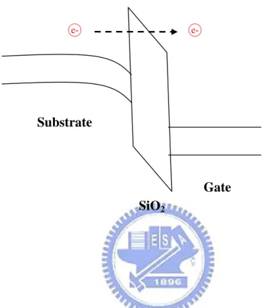
……….eq2.12.2.2 Fowler–Nordheim Tunneling(F-N tunneling)
F-N tunneling show as in Figure 2-2, electrons in the p-type substrate conduction band transfer from trapezoidal to triangular energy barrier. The Fowler–Nordheim (FN) tunneling mechanism occurs when applying a strong electric field (in the range of 8–10MV/cm) across a thin oxide. In these conditions, the energy band diagram of the oxide region is very steep. Therefore, there is a high probability of electrons’ passing through the energy barrier itself. A significant tunnel current can be observed when the tunnel oxide thickness is less than 4nm. However, for thicker tunneling oxide, the electric field is necessary larger or equal to 10MV/cm, the FN tunneling will occurs [22]. The FN tunneling current related formula is shown in Eq. 2-2
ox E B ox
e
E
A
J
−∗
=
2 ………eq 2.22.2.3 Modified Fowler–Nordheim Tunneling
Modified Fowler–Nordheim tunneling (MFN) is similar to the tradition FN tunneling mechanism, yet the carriers enter the nitride at a distance further from the tunnel oxide-nitride interface. MFN mechanism is frequently observed in SONOS memories. The SONOS memory is designed for low-voltage operation (<10V, depending on the Equivalent oxide thickness), a relatively weak electrical field couldn’t inject charges by DT or FN mechanism.
2.2.4 Band to Band Tunneling (BTBT)
Band to band tunneling application to nonvolatile memory was first proposed in 1989. I. C. Chen and et al. demonstrated a high injection efficiency (~1%) method to programming EPROM devices [24]. Band-to-band Tunneling (BTBT) process occurs in the deeply depleted doped surface region under the gate to drain / gate to source overlap region. In this condition, the band-to-band tunneling current density is expressed:
]
3
2
4
exp[
4
2
* 32 2 1 2 3 3h
h
ε
π
q
E
m
E
V
q
m
J
g g app b b=
−
∗ − ………..eq2.32.2.4 (a) Band to Band Hot Electron Tunneling Injection
When band-bending is higher than the energy gap of the semiconductor, the tunneling electron from the valence band to the conduction band becomes significant. The mechanism is at the condition for positive gate voltage and negative drain voltage. Hence, the hot electron are injected through the tunnel oxide and then recombine the stored electrons as shown in Figure 2-3
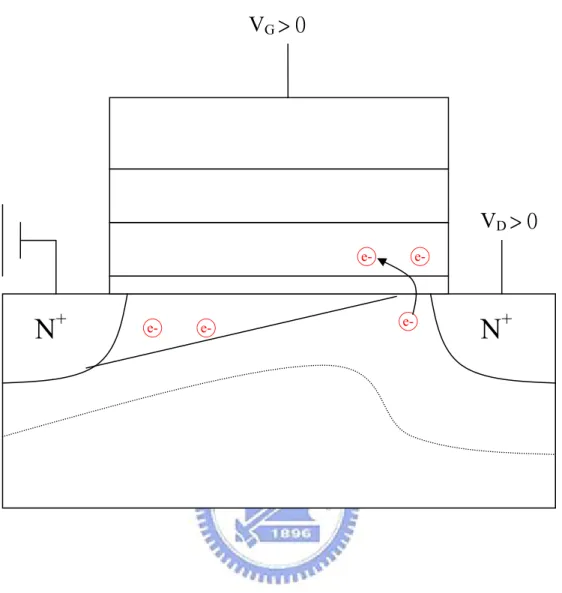
2.2.4 (b) Band to Band Hot Hole Tunneling Injection
The injection is applied for p-type nonvolatile memory device. The mechanism is at the condition for negative gate voltage and positive drain voltage. Hence, the hot holes are injected through the tunnel oxide and then recombine the stored electrons as shown in Figure 2-4.
2.2.5 Trap Assistant Tunneling
The charge storage mediums with many traps may cause another tunneling mechanism. For example, the charges tunnel through a thin oxide and arrive to the traps of nitride layer at very low electrical field in SONOS systems. During trap assisted injection the traps are emptied with a smaller time constant then they are filled. The charge carriers are thus injected at the same distance into the nitride as for MFN injection. Because of the sufficient injection current, trap assistant tunneling may influence in retention [25].
2.3 Nonvolatile Memory Device reliability
Nonvolatility implies at least ten years of charge retention, and the data must be stored in a cell after many read/program/erase cycles. Endurance、retention and distrub experiments are performed to investigate Flash-cell reliability. After that, the conventional scaling problems of flash memory will be discussed.
2.3.1 Retention
In any nonvolatile memory technology, it is essential to retain data for over ten years. This means the loss of charge stored in the storage medium must be as minimal as
possible. For SONOS memory devices, data are represented as electrons stored in the silicon nitride layer, the stored charges leak away from the trapping layer through the tunnel oxide or through the interpoly dielectrics, and the lateral migration of charges trapped in the silicon nitride layer [26]-[27].For example, in modern Flash cells, FG capacitance is approximately 1 fF. A loss of only 1 fC can cause a 1V threshold voltage shift. Possible causes of charge loss are: 1) by tunneling or thermionic emission mechanisms; 2) defects in the tunnel oxide; and 3) detrapping of charge from insulating layers surrounding the storage medium.
During retention, trapped electrons can back-tunnel to the conduction band of the silicon substrate (trap-to-band tunneling), or to the Si–SiO2 interface traps
(trap-to-trap tunneling), under the influence of an internal self-built electric field. Meanwhile, holes from the substrate may tunnel through the thin tunneling oxide and become trapped in the nitride. The retention capability of Flash memories has to be checked by using accelerated tests that usually adopt screening electric fields and hostile environments at high temperature.
2.3.2 Endurance
Endurance is the number of erase/write operations that the memory will complete and continue to operate as specified in the data sheet. Generally speaking, Flash products are specified for 106 erase/program cycles. The endurance requirement is sufficient for the user to take 700 photos with a 1MB size every day for 10 years [27]. As the experiment was performed applying constant pulses, the variations of program and erase threshold voltage levels are described as “program/erase threshold voltage window closure” and give a measure of the tunnel oxide aging [28]-[29]. In particular, the reduction of the programmed threshold with cycling is due to trap generation in the oxide and interface state generation at the drain side of the channel.
The evolution of the erase threshold voltage reflects the dynamics of net fixed charge in the tunnel oxide as a function of the injected charge. The initial lowering of the erase is due to a pile-up of positive charge which enhances tunneling efficiency, while the long-term increase of the erase is due to a generation of negative traps.
The endurance characteristics give the memory threshold voltage window, which is the difference between the threshold voltages in the programmed state and the erased states. It is the parameters to describe how good the reliable is a nonvolatile memory cell. The P/E cycle usually used the FN tunneling or channel hot electron injection mechanism under room temperature environment.
2.4 Summary
Good data retention and endurance and less disturb are an important issue of the SONOS type nonvolatile memory device. These issues affect the scalability of thin dielectric such as tunnel oxide thickness. So the nanocrystal nonvolatile memory are proposed to enhance nonvolatile memory reliability. It’s includes both retention and endurance issue.
Figure 2-1 The diagram of channel hot electrons injection (CHEI)
N
+○
e-○
e-○
e-N
+○
e-○
e-V
G> 0
Figure 2-2 Energy-band representation for explaining FN tunneling.
SiO2
Substrate
Gate
e-Figure 2-3 The diagram of band to band hot electron injection
P-○
e-○
e-V
G> 0
V
D< 0
○
e-P-○
e-○
e-○
h+ Deep Depletion RegionFigure 2-4 The diagram of band to band hot hole injection
N+○
e-○
e-V
G< 0
V
D> 0
○
e-N+○
e-○
h+○
h+ Deep Depletion RegionCHAPTER 3
The experiment process of Pt nanocrystal
and discussion of results
3.1 Introduction
In the past few years, the portable electronic devices have significantly impacted the market of consumer electronics. Because of the low working voltage and nonvolatility, the selection of storage media for most portable electronic devices is the Flash memory which almost bases on the structure of the continuous floating gate (FG) [30]-[31]. In a nanocrystal nonvolatile memory device, charge is not stored on a continue FG poly-Si layer, but instead on a layer of discrete, mutually isolated, crystalline nanocrystals or dots. Also, the nanocrystal memory device can avoid the charge leakage and lower the power consumption when tunneling oxide is thinner[32]-[34]. The self-assembling of silicon or germanium nanocrystals embedded in SiO2 layers has been widely studied, and strong memory effects in MOS devices were reported [32][35][36]. Recently, different charge storage elements have been studied to achieve the robust distributed charge storage[37]-[42]. In this contribution, the Pt nanocrystal was investigated to be a self-assembling layer. The self-assembling layer of Pt nanodot fabricated by the Dual E-gun evaporate deposition system.
Recently, oxynitrides have drawn much attention as a candidate tunnel dielectric for flash memory due to the small charge trapping amount and the low stress-induced leakage current [43][44]. In general, benefit of a silicon oxynitride film is the nitrogen in the film accumulates at the silicon interface to reduce the concentration of strained Si-O bond, potentially reducing the creation of hot electrons by as much as three
orders of magnitude. An oxynitride layer at the Si/SiO2 interface of thin gate oxides
has been found to be beneficial for improving the device electrical characteristic .Nowadays, lower process temperatures and thinner oxynitride films are preferred in ULSI technology.
In this chapter, we proposed a novel approach for forming an oxynitride tunnel dielectric with high nitrogen content. The method was divided into three steps. First, the chemical oxide was nitridation by NH3 in a low-pressure chemical vapor
deposition (LPCVD) reactor. Subsequently, the oxynitride was reoxidation with O2.
By this technique, the oxynitride as the tunnel dielectric and a varying Si-N ratio are obtained. In the oxynitride, we can obtain higher N concentration at the top. The desirable structure can be obtained to meet the requirement of the SONOS type nonvolatile memory device performance. It is noted that the process proposed here is simple and fully compatible with current IC industry fabrication technology.
3.2 Experimental
First, we start our experimental from test nanocrystal capacitor to obtain our experimental condition include anneal temperature、time and gas for nanocrystal memory device process.
3.2.1 Test Nanocrystal Capacitor
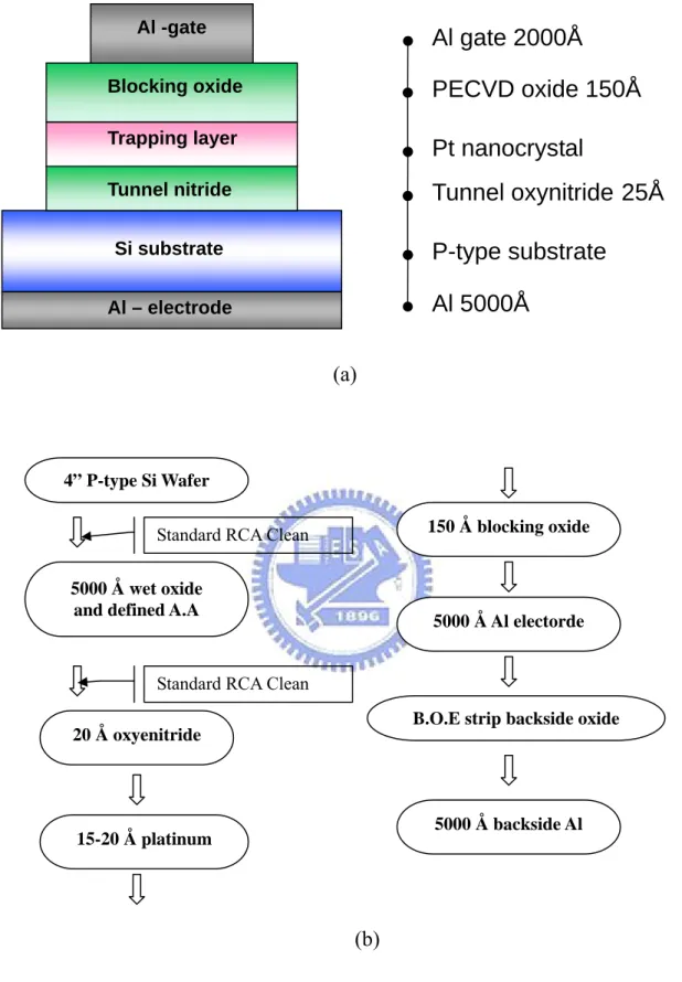
Figure 3-1(a) shows the Pt nanocrystal memory device cross-section. Figure 3-1(b) schematically describes the process flow of the Pt nanocrystal capacitor. Experiments were carried out on 4-inch p-type (100)-oriented silicon wafers with a resistivity of 15-25 Ω cm. Wafers were cleaned using standard RCA cleaning. Before
remove native oxides.
Subsequently, the wafers were immediately immersed into H2O2 solution at room
temperature for 20 min to grow 10Å chemical oxide [45]. The chemical oxide was nitrided by LPCVD in low-pressure (180 mTorr) NH3 ambient at 750℃ for 15 min.
Following that, the chemical oxynitride was placed in atmospheric O2 ambient at 900
℃ 70s and then 15-20 Å Platinum was deposited by Dual E-gun evaporate deposition system. Furthermore about 100Å blocking oxide was deposit by PECVD (Plasma Enhanced Chemical Vapor Deposition ). Afterward, a RTA (Rapidly Temperature Anneal ) system to form nanodot and densification blocking oxide with table3.1.
Finally, a 5000 Å Al metal film was deposited by sputtering. the Al gate was patterned and sintered to form a metal-oxide-insulator-oxide-silicon structure with the insulator combined the Pt nanocrystals. A 5000Å Al film was also deposited on the backside of wafers after stripping the oxide utilizes B.O.E (Buffered Oxide Etcher) on the backside.
A nitrogen distribution profile across the 25Å oxynitride gate dielectric revealed by secondary ion mass spectrometry (SIMS) is shown in Figure. 3-4. Apparently high nitrogen concentration with a peak located at the dielectric surface is observed. The low nitrogen concentration at the interface also improves reliability
3.2.1 Pt Nanocrystal Memory Device
Figure 3-2(a) shows the Pt nanocrystal memory device cross-section. Figure 3-2(b) schematically describes the process flow of the Pt nanocrystal memory device. Experiments were carried out on 4-inch p-type (100)-oriented silicon wafers with a resistivity of 15-25 Ω cm. Wafers were cleaned using standard RCA cleaning. Before growing the chemical oxide film, the wafers were dipped in diluted HF solution to remove native oxides, then to form tunneling dielectric are oxynitride and dry oxide
respectively.
Subsequently, the wafers were immediately immersed into H2O2 solution at room
temperature for 20 min to grow 10Å chemical oxide. The chemical oxide was nitrided by LPCVD in low-pressure (180 mTorr) NH3 ambient at 750 for ℃ 15 min. Following
that, the chemical oxynitride was placed in atmospheric O2 ambient at 900℃ 70s. And
dry oxide about 25 Å is taken shaper inside APCVD(atmospheric pressure chemical vapor deposition) at 900℃ 38s to form tunneling dielectric that we need. Afterward, 15-20 Å Platinum was deposited by Dual E-gun evaporate deposition system. Furthermore about 100Å blocking oxide was deposit by PECVD (Plasma Enhanced Chemical Vapor Deposition ) followed by a N2 densification process at 700℃ for 5
min.
Followed, poly gate 3000 Å is form by LPCVD (low-pressure chemical vapor deposition) at 900℃ for 30 min. Gate pattern defined by lithography, and etching back, then S/D formation by Arsenic dose 5E15 energy 20kev implantation. Continue activation at 950℃ 30s in N2 ambient and covering the passivation layer 5000 Å in
follow up. Then lithograph to define contact hole and B.O.E etching back.
Finally, a 5000 Å Al metal film was deposited by sputtering and lithograph to define metal pad. A 5000Å Al film was also deposited on the backside of wafers after B.O.E stripping the oxide on the backside.
Figure 3-3 schematically describes the construction of measurement system. The electrical characteristics of Pt nanocrystal memory device include test capacitor are measurement by HP4284 Precision LCR Meter and HP4156C Precision Semiconductor Parameter Analyzer.
3.3 Results and discussions
We probe into the characteristic test capacitor and the Pt nanocrystal memory device in this section.
3.3.1 Electrical Characteristic of Pt nanocrystal Capacitor
Figure 3-4(a) shows the capacitance-voltage (C-V) hysteresis of the SONOS
capacitor after RTA 3 minutes at 800℃ in N2 process. When this capacitor is
operated in positive polarity, the electrons directly tunnel from the Si substrate through the tunnel oxide, and are trapped in the Pt nanocrystal. When the capacitor is negatively operated, the holes may tunnel through the tunnel oxide to recombine with electrons trapped in Pt nanocrystal. The blocking oxide is utilized to prevent the carriers of gate electrode from injecting into the charge-trapping layer by FN tunneling. Figure 3-5(a) 、 Figure 3-6(a) and Figure 3-7(a) also shows C-V characteristic at 800℃ 5min N2 anneal、800℃ 3min and 5min O2 anneal separately.
As shown in figure 3-4(a)、figure 3-5(a)、figure 3-6(a)、figure 3-7(a), they are both a counterclockwise direction of the hysteresis, which implies the electrons injected from the deep inversion layer and holes injected from the deep accumulation layer of silicon substrate. Figure 3-4(b)、Figure 3-5(b)、Figure 3-6(b)、Figure 3-7(b) shows the I-V characteristic of 800℃ 3min and 5min N2 anneal、800℃ 3min and 5min O2
anneal separately.
The program characteristic of 800℃ 3min and 5min N2 anneal、800℃ 3min and
5min O2 anneal separately shown in figure 3-4(c)、figure 3-5(c)、figure 3-6(c)、figure
3-7(c). The “Vt shift” is defined as threshold voltage difference between the program
state and erase state. Gate terminals were biased equally from 12 to 16V. As shown in Figure3-4(c) to Figure3-7(c), program characteristics as a function of pluse width.
The erase characteristic of 800℃ 3min and 5min N2 anneal、800℃ 3min and 5min
O2 anneal separately shown in figure 3-4(d)、figure 3-5(d)、figure 3-6(d)、figure 3-7(d).
We observe it when high voltage applied on gate, the band gap bending seriously, the electron through tunneling oxide, and then tunneling through blocking oxide to gate electrode right away. So it’s not very good to cause our performance. The largest memory window is over 1V. Therefore, an optimal asymmetric W/E operating voltage of 12V/-8V at 10ms was determined.
Endurance is the capability of maintaining the stored information after W/E cycling. It is the parameters to describe how good the reliable is a nonvolatile memory cell. The endurance characteristic of 800℃ 3min and 5min N2 anneal、800℃ 3min
and 5min O2 anneal separately shown in figure 3-4(e)、figure 3-5(e)、figure 3-6(e)、
figure 3-7(e). We can observe the endurance performance is better of 800℃ 3min and 5min N2 anneal than 800℃ 3min and 5min O2 anneal. The memory window
degradation of 800℃ 3min N2 anneal don’t exceed 5% after P/E 105 cycle. And the
reason of the memory window degradation is the interface-trap generation. It cause the leakage current becomes large, and deteriorates the quality of the tunnel oxide.
As a result, we observe the best condition of Pt nanocrystal capacitor process is undergo 800℃ 3min N2 anneal. So we take this condition and carried on the Pt
nanocrystal memory device process.
3.3.2 Electrical Characteristic of Pt nanocrystal Device
In this thesis, all devices described had dimensions of L/W=20/50μm. Figure3-8 shows the Id-Vg curve of the oxynitride Pt nanocrystal nonvolatile memory
device under programmed and erased state. Channel hot electron injection and band-to-band hot hole injection were employed for programming and erasing,
also 100ms a memory window can achieve about 0.6V. During programming, a small fraction of electron in the substrate obtain enough energy form applied voltage Vd to
surmount the barrier between tunneling dielectric and silicon conduction band edges. These electrons con be trapped in Pt nanocrystals and the threshold voltage shift to right. When erasing, we applied a positive drain voltage Vd to generate hot hole in the
subject and a large enough negative gate voltage to across the energy barrier. It reduces the threshold voltage and cause the Id-Vg curve shift to left. We use the
mechanism of adjust threshold voltage by different applied voltages to obtain memory characteristics. As a result of the blocking oxide(PECVD oxide) quality is poor. So cause the memory window performance is poor. That because of when the program state the hot electron injection to the nanocrystal, and gate injection hole through blocking oxide to nanocrystal simultaneously. So cause the characteristic of the memory window is not good. Figure3-9 shows the the Id-Vg curve of the oxide Pt
nanocrystal nonvolatile memory device under programmed and erased state. We can observe that actually the oxynitride is actually similar to the characteristic of the oxide.
The oxynitride Pt nanocrystal memory device program and erase spped is shown in figure 3-10. The “Vt shift” is defined as threshold voltage difference between the program state and erase state. Gate and drain terminals were biased equally from 8 to 14V. Both source and substrate terminals were biased at 0V. As shown in Figure 3-10(a) ,program characteristics as a function of pulse width .with Vg
and Vd increasing , the Vth shift increase and the program speed becomes faster. The
figure 3-10(b) shows the erase characteristics of the Pt nanocrystal nonvolatile memory for different conditions. Figure 3-11 also shows the oxide Pt nanocrystal memory device program and erase speed characteristic.
nanocrystal memory device for comparing different temperature (T=25℃、85℃、125 ℃). Figure 3-12 illustrates the retention characteristics of oxide Pt nanocrystal memory device for comparing different temperature (T=25℃、85℃、125℃). The retention time of oxynitride Pt nanocrystal can be up to 108 seconds for about 20% charge loss at room temperature, which is believe to be related to the deep trap energy level in the metal nanocrystal[46]. Further more, the quality of the tunneling oxide plays a significant role in charge retention. It’s a pity that the retention go worst as the temperature increased. We can observe the retention characteristic of oxynitride Pt nanocrystal memory is better than oxide Pt nanocrystal memory.
The endurance characteristics after 105 P/E cycles of the oxynitrde Pt nanocrystal memory device are shown in figure 3-14 and endurance characteristic of oxide Pt nanocrystal memory device are shown in figure 3-15. The programming and erasing conduction are Vg=14v for 100ms and Vg=-8v for 100ms, respectively . Small amount increase of the threshold voltages in programmed and erased state can be observed. This is maybe the stress-induced electron traps generated in the tunneling oxide during cycling[47].
3.4 Summary
In this chapter, we have investigated the memory effects and performance of the Pt nanocrystal memory device. The oxynitride as tunnel oxide will be a candidate for the flash memory in the future. We observe PECVD oxide quality is poor cause our oxynitrde Pt nanocrystal characteristic is not good, but the oxynitride Pt nanocrystal capacitor have large memory window (C-V hysteresis). So we think that Pt nanocrystal is potential application for next generation nonvolatile memory device
memory reliability issue.
The process we proposed is compatible with current CMOS manufacturing technology of semiconductor industry.
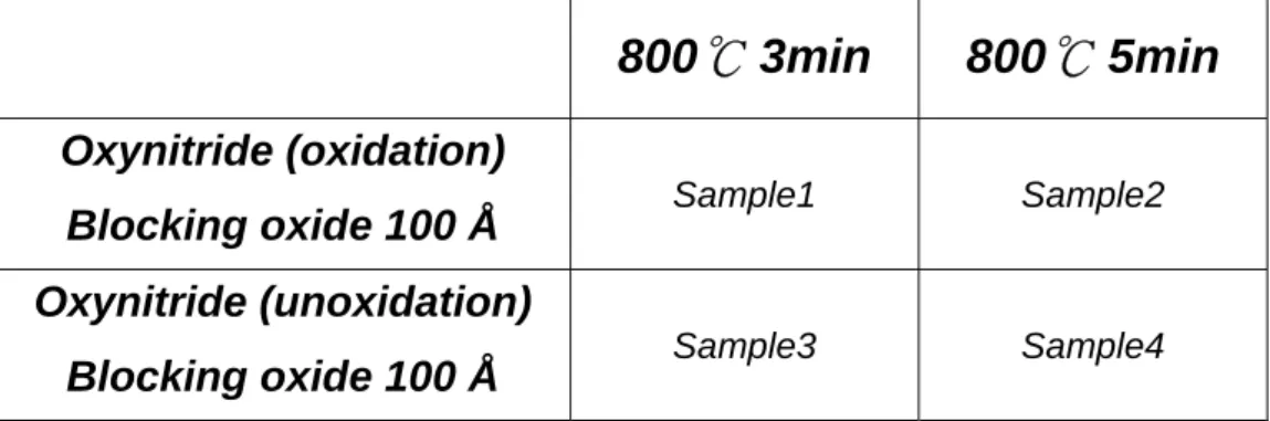
800
℃
3min
800
℃
5min
Oxynitride (oxidation)
Blocking oxide 100 Å Sample1 Sample2 Oxynitride (unoxidation)
Blocking oxide 100 Å Sample3 Sample4
(a)
(b)
Figure 3-1 (a)Schematic cross section of the Pt Nanocrysal capacitor. (b)
Process flows for fabricating various Pt Nanocrysal
capacitors.
Al – electrode Al -gate Blocking oxide Trapping layer Tunnel nitrideSi substrate
P-type substrate
Tunnel oxynitride
25Å
Pt nanocrystal
PECVD oxide 150Å
Al gate 2000Å
Al 5000Å
4” P-type Si Wafer 5000 Å wet oxide and defined A.AStandard RCA Clean
Standard RCA Clean
20 Å oxyenitride
15-20 Å platinum
150 Å blocking oxide
5000 Å Al electorde
B.O.E strip backside oxide
(a)
(b)
Figure 3-2 (a)Schematic cross section of the Pt Nanocrysal Device. (b)
Process flows for fabricating various Pt Nanocrysal Device.
4” P-type Si Wafer
5000 Å wet oxide and defined A.A
Standard RCA Clean
Standard RCA Clean
20 Å oxyenitride
15-20 Å platinum
150 Å blocking oxide
3000 Å Poly gate
Gate pattern and Etch back
S/D implatation 900℃ 30s activation
5000 Å Passivation oxide
Contact hole and Metallization B.O.E strip backside oxide
5000 Å backside Al Tunneling Oxide P-type Si Substrate Control Gate Blocking Oxide Trapping Layer G S D n+ n+ P-type substrate S/D junction formation Tunnel oxynitride 20~25Å Pt nanocrystal PECVD oxide 150Å Poly gate 2000Å
Figure 3-3 The construction of measurement system
Probe Station41501A SMU and Pulse Generation Expender
Switching System HP4156C Precision Semiconductor Parameter Analyzer
HP4284 Precision LCR Meter
0 5 10 15 20 25 30 E17 E18 E19 E20 E21 Depth(nm) Oxygen Nitrogen Poly Si / SiO2 interface
-8 -6 -4 -2 0 2 4 6 0.0 0.2 0.4 0.6 0.8 1.0 800oC 3min N2 Anneal C/C OX VG, Gate voltage [V] Cinvtoacc(8~-8) Cacctoinv(-8~8) (a) -8 -6 -4 -2 0 2 4 6 8 10-13 10-12 10-11 10-10 10-9 10-8 10-7 10-6 10-5 10-4 10-3 800C 3min N2 Anneal Cu rren t [A ] VG, Gate voltage [V] Forward bias Reverse bias (b)
Figure 3-5 (a)The C-V hysteresis of the capacitor with anneal 800℃
3min in N
2process after bidirectional sweeps.(b) The
leakage current of the capacitor with anneal 800℃ 3min in
N
2process.
10-3 10-2 10-1 100 0.2 0.4 0.6 0.8 1.0 1.2 1.4 800oC 3min N2 Anneal V FB S h if t (V ) Programming speed(sec) Program 12V Program 14V Program 16V (c) 10-4 10-3 10-2 10-1 100 -0.2 0.0 0.2 0.4 0.6 0.8 1.0 1.2 1.4 800oC 3min N 2 Anneal V FB Shift ( V )
Erasing speed (sec)
Erase -6V Erase -8V Erase -10V
(d)
Figure 3-5 (c) Program characteristics with different programming
condition.(d) Erase characteristics with different
programming condition
100 101 102 103 104 105 2 3 4 5 -8 -6 -4 -2 0 2 4 6 8 -50.0p 0.0 50.0p 100.0p 150.0p 200.0p 250.0p 300.0p 800C 3min N2 Anneal C, Ca p a c it a n c e [ F ] VG, Gate voltage [V] inv to acc acc to inv inv to acc(105 cycle ) acc to inv(105 cycle ) 800oC 3min N2 Anneal ∆ V th S h ift( V) Cycles pluse width=10ms P/E voltage=8/-8V
Figure 3-5 (e) Endurance characteristics with anneal 800℃ 3min in N
2of the Pt nanocrystal
-8 -6 -4 -2 0 2 0.0 0.2 0.4 0.6 0.8 1.0 Cinvtoacc(8~-8) Cacctoinv(-8~8) 800oC 5min N 2 Anneal C/ C OX V G, Gate voltage [V] (a) -8 -6 -4 -2 0 2 4 6 8 10-12 10-11 10-10 10-9 10-8 10-7 10-6 10-5 10-4 10-3 800oC 5min N 2 Anneal Y Axi s Title X Axis Title Forward bias Reverse bias (b)
Figure 3-6 (a)The C-V hysteresis of the capacitor with anneal
800℃ 5min in N
2process after bidirectional sweeps.(b)
The leakage current of the capacitor with anneal 800℃
5min in N
2process.
10-3 10-2 10-1 100 0.1 0.2 0.3 0.4 0.5 0.6 0.7 0.8 0.9 1.0 800oC 5min N2 Anneal V FB Shift(V) Programming speed(sec) Program 12V Program 14V Program 16V (c) 10-4 10-3 10-2 10-1 100 0.0 0.2 0.4 0.6 0.8 1.0 1.2 1.4 800oC 5min N2 Anneal V FB Shift(V) Erasing Speed(sec) Erase -6V Erase -8V Erase -10V Erase -12V (d)
Figure
3-6 (c)Program characteristics with different programming
condition.(d) Erase characteristics with different
programming condition
100 101 102 103 104 105 0.0 0.5 1.0 1.5 2.0 2.5 -8 -6 -4 -2 0 2 4 6 8 0.0 20.0p 40.0p 60.0p 80.0p 100.0p 120.0p 140.0p 800C 5min N 2 Anneal C , Ca pa c ita nc e [ F ] inv to acc acc to inv inv to acc(105 cycle ) acc to inv(105 cycle ) VG, Gate voltage [V] pluse width=10ms P/E voltage=8/-8V 800C 5min N2 Anneal ∆ Vt h Sh if t(V) Cycles
Figure 3-6 (e) Endurance characteristics with anneal 800℃ 5min in N
2of the Pt nanocrystal
-8 -6 -4 -2 0 2 4 6 8 0.0 0.2 0.4 0.6 0.8 1.0 Cinvtoacc(8~-8) Cacctoinv(-8~8) 800C 3min O 2 Anneal C/ C OX V G, Gate voltage [V] (a) -8 -6 -4 -2 0 2 4 6 8 10-14 10-13 10-12 10-11 10-10 10-9 800 o C 3min O2 Anneal C u rr en t [A] VG, Gate voltage [V] Forward bias Reverse bias (b)
Figure 3-7 (a)The C-V hysteresis of the capacitor with anneal 800℃
3min in O
2process after bidirectional sweeps.(b) The
leakage current of the capacitor with anneal 800℃ 3min in
O
2process.
10-2 10-1 100 0.0 0.1 0.2 0.3 0.4 0.5 0.6 0.7 0.8 0.9 1.0 1.1 1.2 800OC 3min O2 Anneal V FB Shift (V) Programming speed(sec) Program 14V Program 16V Program 18V (c) 10-4 10-3 10-2 10-1 100 -0.1 0.0 0.1 0.2 0.3 0.4 0.5 0.6 0.7 0.8 0.9 1.0 800 O C 3min O2 Anneal V FB Sh ift (V) Erasing time(sec) Erase -8V Erase -10V (d)
Figure 3-7 (c) Program characteristics with different programming
condition.(d) Erase characteristics with different
programming condition
100 101 102 103 104 105 0.0 0.1 0.2 0.3 0.4 0.5 0.6 0.7 0.8 -8 -6 -4 -2 0 2 4 0.0 20.0p 40.0p 60.0p 80.0p 100.0p 120.0p 800C 3min O
2 Anneal inv to acc
acc to inv inv to acc(105 cycle ) acc to inv(105 cycle )
C, C a pa ci ta nc e [ F ] VG, Gate voltage [V] pluse width=10ms P/E voltage=8/-8V 800OC 3min O2 Anneal ∆ V th Shift(V) Cycles
Figure 3-7 (e) Endurance characteristics with anneal 800℃ 3min in O
2of the Pt nanocrystal
-8 -6 -4 -2 0 2 4 6 8 0.0 0.2 0.4 0.6 0.8 1.0
800oC 5min O2 Anneal Cinvtoacc(8~-8)
Cacctoinv(-8~8) C/ C OX VG, Gate voltage [V] (a) -8 -6 -4 -2 0 2 4 6 8 10-13 10-12 10-11 10-10 800oC 5min O2 Anneal Current [ A ] VG, Gate voltage [V] Forward bias reverse bias (b)
Figure 3-8 (a) The C-V hysteresis of the capacitor with anneal 800℃
5min in O
2process after bidirectional sweeps.(b) The
leakage current of the capacitor with anneal 800℃ 5min in
O
2process.
10-3 10-2 10-1 100 0.0 0.2 0.4 0.6 0.8 1.0 1.2 1.4 800OC 5min O 2 Anneal V FB Shi ft (V) Programming speed(sec) Program 12V Program 14V (c) 1E-4 1E-3 0.01 0.1 1 -0.1 0.0 0.1 0.2 0.3 0.4 0.5 0.6 0.7 0.8 0.9 1.0 800OC 5min O 2 Anneal V FB Shift (V) Erasing speed(sec) Erase -8V Erase -10V (d)
Figure 3-8 (c) Program characteristics with different programming
condition.(d) Erase characteristics with different
programming condition
100 101 102 103 104 105 0.0 0.1 0.2 0.3 0.4 0.5 -8 -6 -4 -2 0 2 4 0.0 20.0p 40.0p 60.0p 80.0p 100.0p 120.0p
140.0p 800C 5min O2 Anneal inv to acc
acc to inv inv to acc(105 cycle ) acc to inv(105 cycle ) C, C a p a c ita n c e [ F ] VG, Gate voltage [V] pluse width=10ms P/E voltage=8/-8V 800OC 5min O2 Anneal ∆ Vth Shift(V) Cycles