國 立 交 通 大 學
電子工程學系 電子研究所
碩 士 論 文
利用電流模式的 24-GHz 互補式金氧半
傳送器前端電路
A 24-GHz CMOS Current-Mode
Transmitter Front-End
研 究 生: 許順維 (Shun-Wei Hsu)
指導教授: 吳重雨教授 (Prof. Chung-Yu Wu)
利用電流模式的 24-GHz 互補式金氧半
傳送器前端電路
A 24-GHz CMOS Current-Mode
Transmitter Front-End
研 究 生:許順維 Student:
Shun-Wei
Hsu
指導教授:吳重雨教授
Advisor:
Prof.
Chung-Yu
Wu
國立交通大學
電子工程學系
電子研究所
碩士論文
A Thesis
Submitted to Department of Electronics Engineering and Institute of Electronics
College of Electrical and Computer Engineering
National Chiao-Tung University
in Partial Fulfillment of the Requirements
for the Degree of
Master
in
Electronics Engineering
October 2008
Hsin-Chu, Taiwan, Republic of China
中華民國九十七年十月
i
利用電流模式的 24-GHz 互補式金氧半
傳送器前端電路
研究生: 許順維
指導教授: 吳重雨 博士
國立交通大學
電子工程學系 電子研究所碩士班
摘要
具有高操作頻率高傳輸速率的通訊系統已被視為次世代通訊系統的主軸。在最近 幾年,24-GHz 附近的頻帶中,已有許多頻帶如 24.05–24.25-GHz 的 ISM-band 及 22–29 GHz 被 FCC 釋出作為汽車雷達應用等用途。 此論文中介紹利用電流模式來實現一個操作在 24 GHz 的傳送器前端電路。此傳 送器包含了升頻混波器以及功率放大器等電路並且使用了 0.13-μm CMOS 技術來設 計並製造。藉由電流模式來實現升頻混波器以及功率放大器,使得大訊號操作的傳送 器電路不會受限於 0.13-μm CMOS 的 1.2 V 供應電壓。 此傳送器前端電路包含了升頻混波器以及功率放大器等電路,已被模擬、實現於 1.05 mm2的晶片面積、以及量測。根據量測結果,此電路由於佈局時的錯誤、EM、 製程以及溫度效應的考慮沒有詳盡,使得增益降至 11.5 dB。然而,從修改後的模擬結 果與其它所發表的傳送器電路比較可知,此電路操作在較低的供應電壓下,仍有較好 的線性度。因此,電流模式的電路非常適合用在低供應電壓的製程,尤其是高整合度、 低成本的 CMOS 製程。ii
A 24-GHz CMOS Current-Mode
Transmitter Front-End
Student: Shun-Wei Hsu
Advisor: Dr. Chung-Yu Wu
Department of Electronic Engineering &
Institute of Electronics
National Chiao Tung University
Abstract
In the next-generation wireless communication, high data rate transmission with a high operating frequency is expected to be realized. Over the past few years, the 24.05–24.25-GHz Industrial, Scientific, and Medical (ISM) band, 22–29 GHz band provided by Federal Communications Commission (FCC) for the operation of vehicular radar have been released.
In this thesis, a 24-GHz current-mode transmitter front-end is presented. The proposed transmitter which consists of an up-conversion mixer and a power amplifier is designed using 0.13-μm CMOS technology. By adopting the current-mode approach for design mixer and power amplifier, the large-signal operated transmitter circuit can be implemented under the typical supply voltage 1.2-V of 0.13-μm CMOS technology.
The proposed transmitter front-end, including a mixer and a power amplifier, is simulated, fabricated with a chip size of 1.05 mm2, and measured. Because of the layout mistake, and the effects such as EM, corner and temperature which are not carefully
iii
considered before fabrication, the measured power gain decreases to 11.5 dB. Comparing the results of the re-design transmitter with other proposed transmitter circuits, however, the current-mode transmitter can have better linearity under lower supply voltage. Therefore, current-mode circuits are suitable for low supply voltage technology, especially for high-integrated low-cost CMOS technology.
iv 誌謝 能夠順利畢業,要感謝的人真的很多。首先,我要對我的指導教授吳重雨老 師致上最誠摯的感謝。感謝老師在我碩士生涯中,不論在專業領域上、或是在學 習、做事的態度上,都能給與適時的指導與啟發,使我不在錯誤中打轉,更教導 了我許多做事的方法及應有的態度。 其次,我想對我的口試委員郭建男教授、高宏鑫學長、以及周忠昀學長說聲 感謝,謝謝你們能在雙十國慶恰逢週末的三天連假中,犧牲假期的來為我口試。 也非常感謝在口試中使我受益良多的建議。 接下來我要感謝我的直屬學長王文傑、黃祖德、以及石油王子 Fadi 學長, 他們總是以最嚴謹的態度為我的研究把關,且在我遇到瓶頸時能在很短的時間內 引導我走向正確的方向。實驗室的其他學長余繼堯、蘇烜毅、陳旻珓、羅怡凱、 蔡夙勇、王仁傑、黃建達、廖昌平、郭豐維,以及仿生中心的林俐如、陳勝豪、 楊文嘉、陳煒明......等學長,也常常給我極具建設性的建議,使我的研 究生涯更順利。 再來我要感謝實驗室的同學與學弟妹們:國忠、資閔、松諭巧伶、士豪、維 德、柏宏、廷偉、晏維、國權、威宇、政邦、建名、宗恩、民宗、筱妊、惠雯及 佳琪......等。在這兩年中我們一起研究功課,在失落的時候互相鼓勵, 在被鎖門外時能借住一宿,使我碩士生涯不會有孤軍奮戰的感覺。 另外,我要謝謝我的女朋友凱珺,謝謝你陪我走過我的碩士生涯,再我最失 意的時候,能忍受的我的脾氣並鼓勵著我。 最後,我要謝謝我的家人,謝謝你們無限制的容忍著我的失敗與失落,讓我 感受到無論發生什麼事都有人支持著我,而使我能無後顧之憂的向成功邁進。 其他要感謝的人還有很多,無法一一列出,在此一併謝過。 許順維 于 風城交大 97年 秋
v
A 24-GHz CMOS Current-Mode Transmitter Front-End
Contents
Chinese Abstract
i
English Abstract
ii
Acknowledgement iv
Contents v
Table Captions
vii
Figure Captions
viii
Chapter 1
Introduction
1.1
Background
1
1.2
Motivation
3
1.3
Main Results and Thesis Organization
4
Chapter 2
Review on CMOS Current-Mode RF Front-End
2.1
CMOS Current-Mode RF Receiver
Front-End 7
2.2
CMOS
Current-Mode
RF
Transmitter
Front-End 10
Chapter 3
Circuit Design and Simulation Results
3.1
Design
Consideration
17
3.2
Circuit
Design
17
3.2.1 Up-Conversion Mixer 17 3.2.2 Power Amplifier 23 3.2.3 Transmitter Front-End 313.3
Post-Simulation
Results
33
Chapter 4
Experimental Results
4.1
Chip Layout Descriptions
63
4.2
Measurement
Setup
63
4.3
Experimental
Results
64
4.4
Discussion
65
vi
Chapter 5
Conclusions and Future Work
5.1
Conclusions
101
5.2
Future
Work
102
vii
Table Captions
Table 3.1 Summary of device value 36
Table 3.2 Summary of DC bias 38
Table 3.3 Dimension summary of transmission line 39 Table 3.4 Summary of original post-sim results1 40 Table 3.5 Summary of original post-sim results2 41 Table 4.1 Summary of measurement results 71 Table 4.2 DC consumption for different corners and temperatures 72 Table 4.3 Summary for revised post-sim results 73 Table 4.4 Dimensions summary of the re-design version 74 Table 4.5 Comparison with voltage-mode power amplifier 75 Table 4.6 Comparison with voltage-mode transmitter circuits 76 Table 4.7 Summary table of VREF versus mixer performance 77
viii
Figure Captions
Fig. 1.1 24-GHz service band plan release by FCC 6 Fig. 1.2 Supply voltage (VDD) and threshold voltage (VTH) trends 6
Fig. 2.1 Schematic for current-mode LNA in [12] 11 Fig. 2.2 Schematic for current-mode mixer in [12] 12 Fig. 2.3 Schematic for general concept in [13]–[14] 12 Fig. 2.4 Current-mode direct-conversion receiver proposed in [15] 13 Fig. 2.5 Direct-conversion receiver proposed in [16] 13 Fig. 2.6 Involved block diagram of proposed receiver front-end in [17] 14 Fig. 2.7 Schematic of proposed LNA in [17] 14 Fig. 2.8 Conceptual diagram of proposed down-conversion mixer in [17] 15 Fig. 2.9 Summing circuit of proposed down-conversion mixer in [17] 15 Fig. 2.10 Squaring circuit and band-pass filter of proposed down-conversion
mixer in [17] 16
Fig. 3.1 Block diagram of the designed transmitter front-end 42 Fig. 3.2 Conceptual diagram of the designed mixer 42 Fig. 3.3 Basic operational principle for designed mixer 43 Fig. 3.4 Output waveform for larger ITH 43
Fig. 3.5 Output waveform for smaller ITH 44
Fig. 3.6 Output waveform for extremely large or small ITH 44
Fig. 3.7 Circuit realization for current-adding circuit 45 Fig. 3.8 Circuit realization for self-switching circuit 45 Fig. 3.9 Circuit realization for negative feedback by OPAMP 46 Fig. 3.10 Schematic of the designed mixer 46
Fig. 3.11 Schematic of the OPAMPs 47
Fig. 3.12 Schematic for simulating the characteristic of the feedback loop 47 Fig. 3.13 Simulation results for the characteristic of the feedback loop 48 Fig. 3.14 Input matching network for IF signal 48 Fig. 3.15 Schematic of Gilbert mixer 49 Fig. 3.16 Effect for optimal load when swing is limited 49 Fig. 3.17 Optimal load resistance determined by load-line analysis 49
ix
Fig. 3.18 Neutralization for resonating parasitic CGD 50
Fig. 3.19 Small-signal model of common-source transistor 50 Fig. 3.20 Equivalent network between gate-drain of common-source
transistor 50 Fig. 3.21 Equivalent network between gate-drain of common-source
transistor (L’RES is the combination of LRES and CB) 51
Fig. 3.22 Schematic of designed power amplifier 51
Fig. 3.23 Sweep value of R3 51
Fig. 3.24 Stability factor (k factor) without and with R3 52
Fig. 3.25 Stability meas (b factor) without and with R3 52
Fig. 3.26 Constant POUT, constant PAE contours and the chosen ZLOAD 53
Fig. 3.27 Impedance transformation network of power amplifier 53 Fig. 3.28 Load impedance transferred by transformation network 54 Fig. 3.29 Schematic of designed current-mode transmitter front-end 54 Fig. 3.30 Schematic of designed current-mode transmitter front-end
(with parasitic routing effect) 55 Fig. 3.31 Layout, 3-D model and setting for EM analysis (2-port networks) 55 Fig. 3.32 Layout, 3-D model and setting for EM analysis (3- and 4-port
networks) 55 Fig. 3.33 S-parameter of stand-alone mixer 56 Fig. 3.34 Sweep LO power for stand-alone mixer 56 Fig. 3.35 1-tone test for stand-alone mixer 57 Fig. 3.36 2-tone test for stand-alone mixer 57 Fig. 3.37 S-parameter of 2-stage current-mode power amplifier 58 Fig. 3.38 POUT versus PIN and PAE versus PIN for 2-stage current-mode
power amplifier 58
Fig. 3.39 2-tone test for 2-stage current-mode power amplifier 59 Fig. 3.40 S-parameter of designed transmitter front-end 59 Fig. 3.41 Sweep LO power of designed transmitter front-end 60 Fig. 3.42 Sweep LO frequency of designed transmitter front-end 60 Fig. 3.43 1-tone test for designed transmitter front-end 61 Fig. 3.44 2-tone test for designed transmitter front-end 61
x
Fig. 4.1 Chip microphotograph of the proposed transmitter front-end 78 Fig. 4.2 Measurement setup for the proposed transmitter front-end 78 Fig. 4.3 Sweep IF gate bias through Bias-Tees for checking mismatch 79 Fig. 4.4 Measured S11 of proposed transmitter front-end 79 Fig. 4.5 Measured S22 of proposed transmitter front-end 80 Fig. 4.6 Measured S33 of proposed transmitter front-end 80 Fig. 4.7 Measured gain versus LO input power for proposed transmitter
front-end 81 Fig. 4.8 Measured output power versus LO input frequency for proposed
transmitter front-end 81
Fig. 4.9 Measured output power versus IF input power (1-tone) for
proposed transmitter front-end 82 Fig. 4.10 Measured output power versus IF input power (2-tone) for
proposed transmitter front-end 82 Fig. 4.11 Missing capacitor and the effect in terms of Smith chart 83 Fig. 4.12 Layout view and 3-D model in HFSS for revised post-simulation 83
Fig. 4.13 Temperature measurement 83
Fig. 4.14 S11 of revised post-sim comparing with original post-sim and
measurement 84 Fig. 4.15 S22 of revised post-sim comparing with original post-sim and
measurement 84 Fig. 4.16 S33 of revised post-sim comparing with original post-sim and
measurement 85 Fig. 4.17 Sweep LO power of revised post-sim comparing with original
post-sim and measurement 85
Fig. 4.18 Sweep LO frequency of revised post-sim comparing with original
post-sim and measurement 86
Fig. 4.19 1-tone test of revised post-sim comparing with original post-sim and measurement
86
Fig. 4.20 2-tone test of revised post-sim comparing with original post-sim and measurement
87
xi
Fig. 4.22 The modified layout for re-design transmitter 88 Fig. 4.23 S11 of re-design (SS, 75oC) comparing with original and revised
post-sim 88 Fig. 4.24 S22 of re-design (SS, 75oC) comparing with original and revised
post-sim 89 Fig. 4.25 S33 of re-design (SS, 75oC) comparing with original and revised
post-sim 89 Fig. 4.26 Sweep LO power of re-design (SS, 75oC) comparing with original
and revised post-sim 90
Fig. 4.27 Sweep LO frequency of re-design (SS, 75oC) comparing with
original and revised post-sim 90
Fig. 4.28 1-tone test of re-design (SS, 75oC) comparing with original and
revised post-sim 91
Fig. 4.29 2-tone test of re-design (SS, 75oC) comparing with original and
revised post-sim 91
Fig. 4.30 S11 of re-design (TT, 75oC) comparing with original and revised
post-sim 92 Fig. 4.31 S22 of re-design (TT, 75oC) comparing with original and revised
post-sim 92 Fig. 4.32 S33 of re-design (TT, 75oC) comparing with original and revised
post-sim 93 Fig. 4.33 Sweep LO power of re-design (TT, 75oC) comparing with original
and revised 93
Fig. 4.34 Sweep LO frequency of re-design (TT, 75oC) comparing with
original and revised post-sim 94
Fig. 4.35 1-tone test of re-design (TT, 75oC) comparing with original and
revised post-sim 94
Fig. 4.36 2-tone test of re-design (TT, 75oC) comparing with original and
revised post-sim 95
Fig. 4.37 S11 of re-design circuit in FF, FS, SF, SS, and TT corners 95 Fig. 4.38 S22 of re-design circuit in FF, FS, SF, SS, and TT corners 96 Fig. 4.39 S33 of re-design circuit in FF, FS, SF, SS, and TT corners 96
xii
Fig. 4.40 Sweep LO power of re-design circuit in FF, FS, SF, SS, and TT
corners 97 Fig. 4.41 Sweep LO frequency of re-design circuit in FF, FS, SF, SS, and TT
corners 97 Fig. 4.42 1-tone test of re-design circuit in FF, FS, SF, SS, and TT corners 98 Fig. 4.43 2-tone test of re-design circuit in FF, FS, SF, SS, and TT corners 98 Fig. 4.44 1-tone test by different VREF of proposed mixer 99
Fig. 4.45 1-tone test by different LO input power of proposed transmitter
1
C
HAPTER
1
I
NTRODUCTION
1.1 Background
Recently, the research on radio-frequency integrated circuits (RFICs) in higher frequencies have been accelerated since the frequency spectra below 10 GHz have gradually become crowded by massive requirements of data transmission from the modern wireless applications such as Bluetooth, wireless local area network (WLAN) and ultra-wideband (UWB), etc. Many researchers investigate RF transceiver front-end circuits in 24 GHz because higher operating frequency can provide more bandwidth. In addition, the 24.05–24.25-GHz Industrial, Scientific, and Medical (ISM) band [1], 22–29 GHz band provided by Federal Communications Commission (FCC) for the operation of vehicular radar [2]–[3], and the 24-GHz band plan as shown in Fig. 1.1 [4] are released.
In RF transmitter front-end, key components such as up-conversion mixers and power amplifiers (PAs) have been reported in many CMOS designs [5]–[7]. Nevertheless, in standard CMOS technologies, the active devices have poor inherent characteristics comparing to GaAs and SiGe, and the passive components such as planar inductors have higher losses from lossy substrate. These inherent characteristics seriously degrade the performance of the transmitter front-end circuits. Although the output power of the transmitter can be increased by utilizing multiple parallel transistors to implement power amplifiers [5], the power-added efficiency (PAE) remains the same in such a structure. To improve the PAE, several design techniques
2
have been proposed. By using the special structure of transmission line and additional algorithms, the PAE of a RF CMOS PA can be improved to around 10% [6]–[7].
Besides, the degraded voltage headroom is another challenge. This challenge causes by the decrease of the supply voltage with the scaling and improvement of CMOS technology. The reduction in the supply voltage of modern CMOS technologies originated by the aggressive downscaling of MOS devices has many prominent effects on the characteristics of monolithic CMOS circuits including high packing density, small device parasitic, high device speed, and low power consumption. Unlike supply voltage, the threshold voltage of MOS devices, however, is reduced at a rather slower pace, as shown in Fig. 1.2. As a result, reduced dynamic range and small effective gate-source voltage critically affect the performance of RF circuit implemented by CMOS technologies, particularly those that employ cascode structures.
It is well known that CMOS current-mode circuits have many intrinsic advantages over voltage-mode counterparts including wide bandwidth, tunable input impedances, high slew rates, less susceptible to power and ground fluctuations [8]–[9], low power dissipation, and the most important – lower supply voltage requirement. These characteristics make current-mode circuits particularly attractive for multi-Gbps data communications [10]–[11]. It is because the impedances of internal nodes in current-mode circuits are smaller than those in voltage-mode circuits and the voltage swings at internal nodes are resultant smaller. The signal information, instead of voltage swing in voltage-mode circuit, is mainly carried with the time-varying current signals. Consequently, current-mode circuits can be designed under small voltage headroom. With the above advantages, current-mode RF circuits are capable of
3
operating in low supply voltage and have great potential in the design of CMOS RF front-end in the advanced nanometer CMOS technologies.
1.2 Motivation
This research focuses on a 24-GHz transmitter front-end implemented by CMOS technology. This research also focuses on the novel current-mode approach for designing and implementing this 24-GHz transmitter circuit.
Because of the applications released in 24-GHz frequency range, many researchers are attracted to design high-performance and low-cost wireless applications in this frequency band with advanced CMOS technologies. As mentioned above, however, CMOS technology has limitation of low supply voltage. That is why traditional commercial implementation of wireless transceivers typically utilizes a mixture of technologies in order to implement a high-performance, completed system. Nevertheless, considering the cost and integration capability, CMOS technology is still the most suitable choice for designing RF circuits.
For CMOS technology, the difficulty is to implement a good-performed RF system with low supply voltage constraints. As the CMOS technology is scaled down to nanometer nodes, the supply voltage is gradually reduced to around or even below 1 V. The lower the supply voltage it becomes, the smaller voltage headroom it leaves and the poorer linearity it performs in the design of CMOS RF circuits. The required linearity for transmitter front-end circuit is much higher than that for receiver front-end because of its high power level and resultant large-signal operation is needed. However, low supply voltage constraint and resultant smaller voltage swing directly conflicts with the linearity requirements. That is one of the reasons that more and more
4
transmitter front-end circuits are implemented by other technologies such as GaAs but most of receiver circuits are still realized by CMOS technologies so far. Furthermore, for traditional topologies of RF circuit such as cascoded structures, the lower supply voltage for advanced CMOS technology in the future will not be capable to bias each transistor to a correct biasing point. Because of the advantages of current mode circuit, it has a chance to avoid the limitation of low supply voltage. Besides, when dealing with signal processing, it is easy to perform the function of summation by simply connecting the signal paths together without additional amplifiers. Thus power consumption can be further reduced. Therefore, a current-mode approach is adopted for designing RF transmitter front-end circuit.
1.3 Main Results and Thesis Organization
In this work, the mixer and power amplifier are designed by current-mode circuits. The up-conversion mixer is realized by current-operated self-switching mixer. A 2-stage current-mirror amplifier is proposed for the current-mode power amplifier. Besides, this is the first work in current-mode transmitter for 24-GHz applications. By using the current-mode approach instead of voltage-mode in RF circuit designs, the limitation of lower supply voltage of advanced CMOS technology can be overcome.
The post-sim results of the re-design circuit show that the impedance matching for IF, LO, and RF ports are –5.7, –13.3, and –13.7 dB, respectively. Power gain is 25.2 dB with the LO frequency of 23.9 GHz and IF frequency of 100 MHz. OP1dB is
7.2 dBm and OIP3 is 15 dBm. Power consumption is 314.4 mW from 1.2 V power supply. The performance of stand-alone power amplifier shows it has 22-dB power
5
gain, 11.9-dBm IP1dB, 22-dBm OIP3, 5.5% PAE at 1-dB compression point, and
22.9% peak PAE.
The measurement results show that the measured impedance matching for IF, LO, and RF ports are –1.4, –2.6, and –15.8 dB, respectively. The measured power gain is 11.5 dB with the LO frequency of 21.9 GHz and IF frequency of 100 MHz. Measured OP1dB is –9.5 dBm and OIP3 is 4 dBm. The total power consumption is 238.4 mW
from 1.2-V power supply. Comparing to other voltage-mode work [6][23][24], the proposed current-mode transmitter has better linearity and lower power dissipation under lower supply voltage. The experimental results and comparisons show that current-mode circuits are suitable for low supply voltage technology, especially for advanced CMOS technology.
The thesis is divided into five chapters. Chapter 1 introduces the background, motivation and main results of this research. Chapter 2 will discuss the concept of current-mode and the published current-operated RF front-end circuits.
The current-mode transmitter front-end of this thesis will be presented at Chapter 3. Design consideration of the transmitter front-end is discussed in Section 3.1. Then the power amplifier, up-conversion mixer, and the transmitter front-end design procedures are presented in Section 3.2.1, 3.2.2, and 3.2.3, respectively. Post-simulation results are shown in Section 3.3.
The chip microphotograph, measurement setup, experimental results, revised post simulation and re-design will be included in Chapter 4. Finally, the conclusions and future work will be presented in Chapter 5.
6
Fig. 1.1 24-GHz service band plan release by FCC.
7
C
HAPTER
2
R
EVIEW ON
CMOS
C
URRENT
-M
ODE
RF
F
RONT
-E
ND
2.1 CMOS Current-Mode RF Receiver Front-End
A current-mode receiver front-end is proposed in [12], as shown in Fig. 2.1–Fig. 2.2. The current-mode low-noise amplifier (LNA) is shown in Fig. 2.1. In order to adopt current-mode methodology, the first stage is a transconductance stage which makes an I-V conversion. The converted current signal then passes the current-mirror amplifier for second stage. Besides, this proposed LNA also adopts capacitive feedback match for input matching network in order to minimize the noise figure and maximize power gain simultaneously. The current-mode mixer shown in Fig. 2.2 is realized by current-operated self-switching mixer. This current-mode receiver has the advantages of low supply voltage and low power consumption.
Current-mode related down-conversion mixers are in [13]–[14]. These two mixers are proposed with a novel concept for realizing mixing function by current-mode operation. The schematic for general concept of these two mixers are given by Fig. 2.3. By using current inputs instead of voltage inputs, all series-connected transistors can be replaced by parallel-connected transistors in order to reduce the number of the cascode transistors. The detailed equations derived in [13] show that the differential output current (iIF+ – iIF–) is proportional to the multiplication
of iRF and iLO. Thus the mixing function can be done by this operation. Because of
non-cascode structure, this current-mode mixer has the capability of low supply voltage operation.
8
Schematic shown in Fig. 2.4 is another current-mode receiver proposed in [15]. This proposed circuit modifies the receiver shown in Fig. 2.5 [16]. Since the circuit in Fig. 2.4 suffers from the problems of less degree of freedom for optimization and enough supply voltage is required for cascode structure. The modified current-mode receiver avoids these limitations by separating LNA from the tail current source in the mixer. Because only the RF current output from LNA to mixer, the bias currents for the LNA and the mixer are separated. The separated bias allows independent optimization for the noise in these two blocks. Besides, the headroom requirements are also relaxed in this circuit because the tail current source in the mixer does not govern the linearity.
Another current-mode receiver front-end including a LNA and a down-conversion mixer is shown in Fig. 2.6 [17]. This proposed current-mode LNA is consisted of a two-stage cascaded current mirror to amplify current signal. By adding diode-connected PMOS to reduce effective supply voltage shown in Fig. 2.7, this LNA can be operated correctly by lower than 1.2 V, the typical supply voltage for 0.13-μm CMOS technology. It means this proposed topology has potential for designed RF circuits by advanced CMOS technology in the future.
The concept of this proposed current-mode down-conversion mixer comes from square law. The conceptual block diagram of this proposed current-mode down-conversion mixer is depicted in Fig. 2.8. This mixer is composed of a current summing circuit, a current squaring circuit, and a band-pass filter (BPF). The RF input current signal
ilna = ILNAcosωRFt
9
ilo = ILOcosωLOt
from the off-chip LO signal generator are summed in advance through the current summing circuit. The summed current signal
isum = (ilna + ilo) = (ILNAcosωRFt + ILOcosωLOt)
are sent to the following current squaring circuit which results in the square components of i2lna and i2lo and the multiplication component ilna × ilo. The
multiplication component of two current input signals provides the function of double-sideband mixing. Through the double-sideband mixing, the received 24-GHz signal is converted to 5 GHz which is the lower sideband (LSB) and 43 GHz which is the upper sideband (USB) with the LO signal at 19 GHz. Following the current squaring circuit is the BPF which is capable of frequency selectivity. In this receiver design, the center frequency of the BPF is designed at 5 GHz so that the targeted LSB can be obtained and the unwanted USB can be attenuated. Fig. 2.9 shows the current summing circuit. Two common-gate transistors M8 and M9 operated in the saturation
region function as current buffers. Due to the advantage of current-mode signal processing, the adding function can be realized by wired connection without any extra circuits. Thus the current signals iout,lna from LNA circuit and iin,lo from off-chip LO
signal generator are summed by directly connecting the drains of M8 and M9 together.
The conceptual circuit of other parts is implemented as shown in Fig. 2.10. A current-mirror structure is adopted so that the squaring function can be realized by the transistor’s square law. The following band-pass filter is implemented by a LC tank that can filter out all frequency of signal except desired 5-GHz band. The detailed operational principles of the current summing circuit and the current squaring circuit are described in [17]. This current-mode receiver has the advantage of smaller power
10
dissipations and can be operated in low supply voltage. Besides, this current-mode receiver front-end also has better linearity performance.
According to these current-mode receiver front-end circuits illustrated above, no cascoded transistor is needed except the diode-connected transistors which are for reducing the effective supply voltage. Thus current-mode approach is a suitable solution for insufficient headroom problem caused by lower supply voltage of advanced technologies.
2.2 CMOS Current-Mode RF Transmitter Front-End
The transmitter front-end, o the other hand, consists of up-conversion mixer and power amplifier. Like the receiver front-end, the up-conversion mixer can also be realized by square-law or self-switching concept.
The current-mode up-conversion mixer proposed in [18] is the same concept of square-law as down-conversion mixer proposed in [17] but double-balance structure. Because of the advantage of current approach, the summing function is realized by directly wired connection. Thus a huge number of amplifiers or other extra circuits are preserved and the lower power consumption and smaller chip area are achieved.
Another up-conversion mixer at RF frequency of 2 GHz proposed in [19] adopts current-operated self-switching concept that the mixing function can be implemented under lower supply voltage. The detailed concept will be explained in chapter 3.
A current-mode power amplifier which is implemented by standard 0.13-μm CMOS technology is proposed in [20]. Because the specifications are different for preamplifiers and power amplifiers, this current-mode power amplifier is similar but
11
not completely the same with the preamplifier. First, two n-type current-mirror stages are adopted and current feedback is removed because of the PAs’ high power gain requirement. Second, according to the required high output power, DC current of output stage cannot be reduced. Thus the low-power design proposed in [21] is not suitable for power amplifier. Besides, because of the serious parasitic by large transistors’ size at high frequency, a neutralized method is implemented by current-mode power amplifier in [20]. This proposed current-mode power amplifier consists of two-stage cascaded current-mirror structure, two neutralized LGD between
gate-drain for both stages, and load-pull analysis for output transformation network (output matching network). This CMOS power amplifier can perform saturated output power as large as 20 dBm. Besides, it also shows that no cascode are necessary for implementing power amplifier by current-mode approach. Therefore, these current-mode circuits show that it is possible to implement CMOS transmitter front-end by current-mode approach.
12
Fig. 2.2 Schematic for current-mode mixer in [12]
i
LO+i
LOi
RF+i
RFI
REFI
REFI
REFi
IFi
IF+V
DD13
IF
OUTLO
INLO
+INBIAS
BIAS
RF
INV
DDFig. 2.4 Current-mode direct-conversion receiver proposed in [15]
RF
INLO
+INLO
INIF
OUT14
Fig. 2.6 Involved block diagram of proposed receiver front-end in [17]
15
( )
2(i
lna+i
lo)
(i
lna+i
lo)
2i
ifi
loi
lna+
+
Current
Summing Circuit
Current Squaring
Circuit
Bandpass
Filter
Mixer
Fig. 2.8 Conceptual diagram of proposed down-conversion mixer in [17]
iout,sum iin,lo iout,lna Zrfin,SUM Zloin,SUM SUMOUT LOIN RFIN C5 C6 CPAD2 L4 L5 L6 M8 M9 VDD
16
i
OUTi
2i
3i
1i
inM
SQ1M
SQ2M
SQ3C
7L
7Bandpass
Filter
Current Squaring
Circuit
V
DDFig. 2.10 Squaring circuit and band-pass filter of proposed down-conversion mixer in [17]
17
C
HAPTER
3
C
IRCUIT
D
ESIGN AND
S
IMULATION
R
ESULTS
3.1 Design Consideration
In this research, as shown in Fig. 3.1, a current-mode transmitter front-end included an up-conversion mixer and a power amplifier is realized with 0.13-μm CMOS technology. The designed mixer is implemented by the current-operated self-switching concept in order to compromise with the typical supply voltage of 1.2 V for standard 0.13-μm CMOS technology. The power amplifier which is also realized by current-mode concept consists of two stages to provide larger than 20-dB power gain. The 1st-stage of power amplifier amplifies the RF signal comes from designed mixer to drive the 2nd-stage of power amplifier. The 2nd-Stage is designed to have capability to provide enough signal swing that the required output power can be achieved. The specification of the designed transmitter front-end is to output more than 10-dBm output power at 24 GHz.
3.2 Circuit Design
3.2.1 Up-Conversion MixerThe concept of the current-operated self-switching up-conversion mixer comes from [19]. The concept diagram of the designed mixer is shown in Fig. 3.2. Two current signals of IF and LO are summed together. The summed current signal is then passed through the self switch. This switch is called self switch because the summed current signal is not only its input but its control signal. Therefore, the switch is turned
18
on if the level of the summed current signal is larger than turn-on threshold current ITH
of the switch. Therefore, only the current signal larger than ITH is appeared at the
output of the switch. The fully balance structure which is composed of Path-A and Path-B is selected to eliminate non-ideal effect. Consequently, the mixing function can be achieved, and it can be applied to realize a differential up-conversion mixer.
The operation principle in terms of waveform for this designed mixer is illustrated in Fig. 3.3. According to the Fig. 3.2, the input signals are one low-frequency current signal IF (iif+ or iif–) and one high-frequency current signal LO (ilo+ or ilo–) in each path,
as shown in Stage-I in Fig. 3.3. The adding signal (iif+ + ilo+ or iif– – ilo–) shown in
Stage-II is the linear combination of these two current signals. The output signals of self switch (irf1 and irf2) are given by the Stage-III. Because of the characteristics of the
self switch, the specific period of waveform that their amplitudes are larger than the ITH will be remained and pass through the self switch. After linear combined these two
signals, the mixing function can be done as shown in Stage-IV. Larger (Fig. 3.4) or smaller ITH (Fig. 3.5) will produce worse performance. The extremely case is shown in
Fig. 3.6. The switches always turn off or turn on and the resultant output is eliminated. Therefore, the biasing condition must be carefully considered in order to guarantee the ITH level the same as in Fig. 3.3.
The detailed description is derived in (3.1)–(3.8). The Path-A and Path-B signals in Stage-I are shown in (3.1)–(3.2), respectively. In (3.1), A is the amplitude of the IF signal, ωIF is the frequency of the IF signal, B is the amplitude of LO signal, and ωLO is
the frequency of the LO signal. The adding signals in Stage-II are (3.3)–(3.4). After the adding signals of IF and LO go through the self switch, the output signals of the switch,
irf1(t) and irf2(t), can be regarded as the adding signals multiplied by repeating 1,0,1,0,...
19
expressed as (3.5) where the IF and LO signals are given by (3.1). Similarly, signal
irf2(t) in path-B can be expressed by (3.6). Thus the adding signal irf(t) (= irf1(t) + irf2(t))
in Stage-IV can be expressed by (3.7), just like the mixing waveform irf(t) illustrated in
Fig. 3.3. After output LC tank, the output signal remains only the mixing term in (3.8). According to the equations above, it is obvious that this mixing concept can be implemented in current-mode operation.
( )
( )
if IF lo LO i + t =A sin ω t, i + t =Bsin ω t (3.1)( )
(
)
( )
(
)
if IF lo LO i − t =A sin ω t π , i+ − t =Bsin ω t π+ (3.2)( )
( )
if lo IF LO i + t +i + t =A sin ω t Bsin ω t+ (3.3)( )
( )
(
)
(
)
if lo IF LO i − t +i − t =A sin ω t π + +Bsin ω t π+ (3.4)( ) (
)
rf 1 IF LO LO LO 2 π 1i t A sin ω t Bsin ω t sin ω t sin 3ω t H.O.T.
π 4 3 ⎛ ⎞ = + × ⎜ + + + ⎟ ⎝ ⎠
(
)
2 IF LO LO IF LO 1 2B 2AA sin ω t Bsin ω t sin ω t sin ω t sin ω t H.O.T.
2 π π = + + + + (3.5)
( )
(
)
(
)
(
)
(
)
rf 2 IF LO LO LO i t A sin ω t π Bsin ω t π 2 π 1sin ω t π sin 3 ω t π H.O.T.
π 4 3 =⎡⎣ + + + ⎤⎦ ⎡ ⎤ × ⎢ + + + + + ⎥ ⎣ ⎦
(
)
2 IF LO LO IF LO 1 2B 2AA sin ω t Bsin ω t sin ω t sin ω t sin ω t H.O.T.
2 π π
= − + + + + (3.6)
( )
2rf IF LO LO
4A 4B
i t sin ω t sin ω t sin ω t H.O.T.
π π = + + (3.7) IF LO 4A sin ω t sin ω t π (3.8)
20
The circuit realization is given by Fig. 3.7–3.9. I-V transfer and current-adding circuits are shown in Fig. 3.7. I-V transfer-function for IF and LO signals are implemented by PMOS (M1) and NMOS (M2), respectively. Because of the
current-mode operation, these two current signals are added at the drain terminal of M1
and M2 (node A1) in a wired-OR manner without any extra circuits. Comparing to two
common-source NMOS, the DC current can be re-used and resultant power consumption of whole transmitter front-end can be lower. The self-switching function is realized by M3 in Fig. 3.8, where the iif+(t) and ilo+(t) are given in (3.1) and IIFB/ILOB
is the DC current of IF/LO.
The source terminal of the transistor M3 is also connected to this terminal. IIFB and
ILOB are set to IIFB = –ILOB so that M3 is turned off when iif+(t) and ilo+(t) are not applied.
This condition means ITH = 0 in Fig. 3.2 and Fig. 3.3. Furthermore, M3 is turned on
when IF and LO signals are input and iif+(t) + ilo+(t) > 0. This indicated that the
transistor M3 detects the polarity of iif+(t) + ilo+(t) and is switched on by the polarity. In
this way, the current adding and self-switching circuits is realized using current-mode operations.
Because of the characteristics of self-switching transistor M3, any drifted ITH level
result in the VGS of switch transistor M3 will affect its characteristic and degrade the
performance of this mixer as shown in Fig. 3.4–Fig. 3.6. Thus some extra circuits are adopted in order to fix the biasing point of the internal node A1. The negative feedback
is realized by OPAMP, as shown in Fig. 3.9.
The schematic of the designed mixer is shown in Fig. 3.10. The IF and LO frequency are 100 MHz and 23.9 GHz, respectively, in this designed mixer. M1,4 and
M2,5 are operated in the saturation region and functioned as transconductors that
21
conversion gain, “VDD/2” is chosen for VA1 and VA2, the DC bias of the internal nodes
A1 and A2. The gate biasing points for these four transconductors are chosen by the
optimal linearity for each of them. The gate-to-source voltage of M3 and M6, VGS3 and
VGS6, are designed to equal to their respective threshold voltage VTH3 and VTH6 such
that the characteristic of self switch can be achieved. Because the different value of VGS, no matter higher or lower, will reduce amplitude of output RF signal, the VGS of
M3 and M6 must be fixed. The DC biases VB1 and VB2 are carefully designed in order
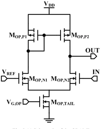
to achieve the condition of VGS=VTH. Besides, two operational amplifiers (OPAMPs)
with the configuration of differential input single-ended output shown in Fig. 3.11 are used to implement negative feedback loops so that the DC bias of the internal nodes VA1 and VA2 are virtual short to the biasing voltage VREF. Therefore, the DC biasing
points of the sources of M3 and M6 can be fixed, and the voltage of VREF is chosen as
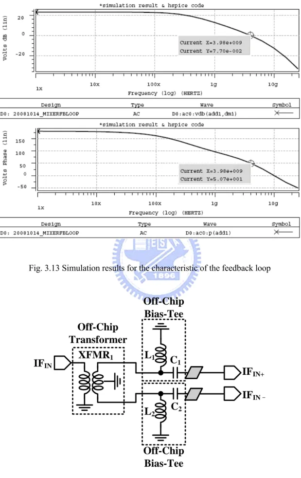
VREF=VB2–VTH3,6. The schematic and the results for simulating this feedback loop are
shown in Fig. 3.12 and Fig. 3.13, respectively. According to Fig. 3.13, the phase margin of this loop is large than 50o.
For transconductors M1,4 and M2,5, larger size of them can provide larger
transconductance. In RF systems, however, serious parasitic effect comes up with large transistor’s size. For low-IF or direct conversion receiver front-end circuits, it can be resonated out simultaneously by only one inductor because the frequency of input signals RF and LO are almost the same. Unfortunately, this situation will never occur in transmitter front-end unless the impractical specification that IF and LO frequencies are exactly equal to half of the RF frequency. That is, the IF and LO frequencies are too different to simultaneously resonate out the parasitic capacitance at nodes A1 and
A2 simultaneously. Therefore, large transistor provides large transconductance, but a
22
any parasitic capacitance can be regarded as an equivalent short path for high frequency, it may degrade RF signal by leakage RF signal to ground. The optimized sizes of these four transistors are determined by largest amplitude of current signals after I-V conversion.
In order to provide lower impedance that the adding signal of IF and LO can easily flow into self-switching circuit, the dimension of self-switching transistors M3
and M6 are designed as large as possible. However, just like the transconductance
transistors, these self-switching transistors are suffered from the same situation that large size can provide lower impedance for adding signal but serious and un-removable parasitic problem at their source terminals. The sizes of these two transistors are optimized by the largest current amplitude of RF signal at output node of mixer.
The LO input matching network is composed of R1, R2, XFMR2, C3, and the
parasitic capacitance of the LO input pad CPAD3. Input matching network for 100-MHz
IF signal is not integrated on chip. Instead, as shown in Fig. 3.14, two off-chip biased-tees (C1, C2, L1 and L2) and an off-chip transformer (XFMR1) are required
during measurement. The inductor L3 and parasitic capacitance at output node, drain
terminals of M3 and M6, are implemented for output LC tank that functions as a filter
and only passes desired RF signal to power amplifier.
The voltage headroom required at the nodes A1 and A2 is “2×VDSAT +ΔV”, which
ΔV is signal voltage swing. It is the same as the nodes B1 and B2 in conventional
Gilbert mixer shown in Fig. 3.15. In Gilbert mixer, however, the output node is high impedance node and directly proportional to its conversion gain. Thus the voltage swing at the output node of Gilbert mixer must be large. In designed current-operated self-switching mixer, the node A1 and A2 are low impedance nodes because that the
23
sizes of M3 and M6 are large enough so that the current signal can pass though them.
Because the signal information is mainly carried by the current swing, the voltage swing is much smaller that that in Gilbert mixer. That is, the required ΔV is much smaller than that in Gilbert mixer. Comparing with the conventional Gilbert mixer, consequently, the designed current-operated self-switching mixer has better linearity if the supply voltage is the same, or supply voltage can be reduced if the linearity specification is the same. Thus the self-switching mixer in current-mode approach has great potential to operate in low supply voltage in advanced nanometer CMOS technology.
3.2.2 Power Amplifier
As to power amplifier, the most critical node is its output because high output power and resultant large voltage and current swing are required. Large output power which implies to large DC bias means the reliability such as metal current density must be considered. Besides, large voltage and current swing which implies to large-signal operation must be considered instead of small-signal operation. Therefore, for RF systems’ power amplifiers, the output impedance transformation networks (output matching networks) are always implemented by load-line or load-pull analysis instead of traditional conjugate match.
The traditional conjugate match can provide maximal power transfer only under the condition of no current and voltage swing limitation. It is always true for small-signal operation. That is why most of RF systems, such as receiver, adopt traditional conjugate match for their matching networks. However, transmitter front-end, especially for output of power amplifier, is large-signal operation. It is because that power amplifiers always produce high output power, the current or voltage swing always reaches the limitation of its supply. Therefore, instead of
24
traditional conjugate match, the output matching networks of power amplifiers are usually determined by two methods – load-line or load-pull.
A quantitative description is given by Fig. 3.16 for the difference of optimal load if the voltage and current swing are limited. For traditional conjugate match, the load resistance RL is chosen to equal to RS. If the voltage and current swing are limited,
however, it is clear that the “VMAX/IMAX” load resistance have maximal output power
than any other load resistance.
The load-line analysis on a common-source transistor I-V curve is illustrated in Fig. 3.17. The load-line shown by black color is the optimal load resistance determined by load-line analysis. It is obvious that the load-line has maximal output power under this voltage and current swing limitation. Any load resistance which is smaller than the optimal resistance will have the same current swing but smaller voltage swing and resultant smaller output power. Any load resistance which is larger than the optimal resistance will have the same voltage swing but smaller current swing and resultant smaller output power. The hand-calculated procedure for load-line analysis can be accessed through (3.9)–(3.10). The transistors’ sizes (in terms of DC current) and optimal load resistance can be calculated as long as the required output power is given.
(
)
OUT,MAX DC knee DC 1 P V V I 2 = − (3.9) DC knee L,OPT DC V V R I − = (3.10)25
From the figures and equations of load-line analysis above, it is not difficult to notice that load-line analysis can be used for quickly determining optimal load resistance, but not reactance. Because load-line analysis bases on I-V curve, the junction parasitic effect is exclusive. That is, only the real part of the load impedance (ZL) can be determined by this analysis, the effect of imaginary part cause by the
parasitic effect of the circuit will be completely neglected. Unfortunately, the parasitic effect induce lose for high frequency signal. Besides, the larger size of the transistor it is, the parasitic effect is worse and cannot be ignored.
Comparing to load-line, load-pull analysis can be used to determine the load impedance ZL, both real and imaginary part, of power amplifiers. The load-pull
analysis, shortly, is to sweep ZL to see how PAs perform. The analysis procedure is:
First, add a load tuner at the output of power amplifier. Second, sweep the value of load tuner (ZL) to see the difference of output power (POUT) and PAE. Because of each
point on Smith chart is a reflection coefficient, and the reflection coefficient and impedance are one-to-one mapping for 50-ohm characteristic impedance, the swept data can be used to construct constant POUT and constant PAE contours. Third, choose
one reflection coefficient (load impedance) on Smith chart by trade-off between constant POUT and constant PAE contours. Using load-pull analysis to determine ZL
has several advantages. Because the constant POUT and PAE contours are drawn on the
same Smith chart, it is easy and obvious to trade-off between them. Besides, because of the one-to-one mapping characteristic, both real and imaginary part of ZL can be
determined as soon as the trade-off point has been chosen.
Another difficulty for designing power amplifier is the parasitic effect. Because high output power is required, a cumbersome size of each transistor and resultant seriously parasitic effect are inevitable. Large parasitic capacitance CGD provides a
26
short path between input and output at high frequency in common-source amplifier. Therefore, a resonated inductor (LRES) must be used between these two nodes shown in
Fig. 3.18 for resonating parasitic capacitance CGD and improving reverse isolation.
The small-signal model for a common-source amplifier is shown in Fig. 3.19. Because the S-parameter S12 is desired, input phasor E2 is placed at port 2 (drain).
According to the definition of S12 shown in (3.11) [22], the term “VO1/E2” can be
expressed by (3.12). Although (3.11) and (3.12) can show the effect for value of ZX, it
is not obvious. In order to further simplify this equation, the matched condition at output node is assumed. This condition is always true for RF systems. The S22 of common-source amplifier can be calculated through (3.13) to (3.14). α and β are the substituted variables for the numerator and denominator in (3.13), respectively. Under the matched condition, the condition “ZO2β=α” can be derived as shown in (3.15).
Thus (3.12) can be further simplified by this derived condition and the final result for S12 of common-source amplifier is shown in (3.16).
For a traditional common-source amplifier, ZX is “1/jωCGD” and S12 will become
(3.17). Thus larger the transistor size it is, larger the value of parasitic capacitance CGD
it has and worse the reverse isolation it becomes. For extremely case of infinitely large CGD value, the S12 will become the equation shown in (3.18) and equal to 1 (or 0 dB)
in general for RF circuits (for ZO1 = ZO2 = ZO = 50 ohm, general case in RF circuits).
0-dB S12 means this circuit has no any reverse isolation or the equivalent circuit for this two-port network is short circuit. It is reasonable because the infinitely large CGD
provides a zero-impedance short path between port-1 and port-2.
If the resonated inductor LRES is adopted and placed between gate-drain, the
27
condition in (3.20) is achieved. That is the reason why a resonated inductor is always adopted for large-sized common-source amplifier.
O2 O1 2 O1 Z V S12 2 E Z ≡ × × (3.11) ( ) ( ) ( ) ( ) O1 O1 GS DS 2 O2 m O1 GS DS X O1 X GS O1 GS O1 DS GS DS DS X O1 X GS O1 GS V Z Z Z E =Z ×⎣⎡g Z Z Z + Z Z +Z Z +Z Z + Z Z +Z Z ⎤⎦+Z × Z Z +Z Z +Z Z (3.12)
(
)
(
) (
DS X O1 X GS O1) (
GS)
T2 m O1 GS DS X O1 X GS O1 GS O1 DS GS DS Z Z Z Z Z Z Z Z g Z Z Z Z Z Z Z Z Z Z Z Z Z × + + = + + + + + (3.13) T2 O2 O2 T2 O2 O2 Z - Z α - Z β S22 Z Z α Z β ≡ = + + (3.14) O2 S22→ ⇒0 Z β α= (3.15) O2 O1 O2 O1 GS DS 2 O2 O1 O1 Z V Z Z Z Z S12 2 2 E Z β α Z Z ⎛ ⎞ ≡ × × =⎜⎜ × ⎟⎟× + ⎝ ⎠(
)
O2 O1 GS DS X O1 DS GS DS O1 GS DS O1 Z Z Z Z Z Z Z Z Z Z Z Z Z ⎛ ⎞ =⎜⎜ ⎟⎟× + + ⎝ ⎠ (3.16)(
)
O2 O1 GS DS O1 O1 DS GS DS O1 GS DS GD Z Z Z Z S12 Z 1 Z Z Z Z Z Z Z jωC ⎛ ⎞ =⎜⎜ ⎟⎟ ⎛× ⎞ ⎝ ⎠ ⎜ ⎟× + + ⎝ ⎠ (3.17)28 O2 O1 Z S12 Z ≈ (3.18) RES X RES 2 GD RES GD jωL 1 Z jωL // jωC 1 ω L C = = − (3.19) 2 RES GD X if ω L C = ⇒1 Z → ∞ ⇒S12→ 0 (3.20)
For RF system, an ideal inductor is equal to a short path for DC because its impedance is “jωL”. Therefore, as long as the resonated inductor is implemented, a blocking capacitor is always used for blocking unnecessary DC path. This blocking capacitor, CB, comes from the consideration during measurement. The cable inherent
resistance between probe and DC power supply is around 3 ohm. It’s not a serious issue for small-signal systems such as receiver front-end. However, for hundreds milli-ampere transmitter front-end, it may cause milli-volt or even several volts drop during measurement. Because such voltage drop may downgrade internal biasing points by different levels, DC current may be sunk into unexpected path when measurement. In order to avoid this phenomenon, a capacitor must be added to block DC current from stage to stage.
Fig. 3.20 is the equivalent network between gate-drain of common-source transistor. Because CB is used for DC blocking, its value is much larger than parasitic
capacitance CGD and the resonating frequency of LRES and CB is much lower than the
resonating frequency of LRES and CGD. After the resonating frequency of LRES and CB,
the series LRES and CB can be equivalent to an inductance L’RES and its value is shown
in (3.21). Therefore, the equivalent network between gate and drain can be express in Fig. 3.21. The impedance between gate and drain in Fig. 3.21 is given by (3.22). Thus
29
if the inductance value must be chosen to satisfy the condition in (3.23), the parasitic capacitance can be resonated and the reverse isolation can be improved.
' RES RES 2 B 1 L L ω C = − (3.21) ' ' RES RES 2 ' GD RES GD jωL 1 jωL // jωC =1 ω L− C (3.22) ' RES GD 1 ω L C = (3.23)
Shown in Fig. 3.22 is the designed 2-stage cascaded current-mode PA that has been published by the present author [20]. The proposed PA consists of two cascaded current-mirror amplifiers to amplify the current signal.
By (3.9)–(3.10), the transistors’ dimensions and optimal load resistance can be roughly predicted by hand calculation. Two stages are adopted for the budget of PA’s output power and power gain. Because the biasing is fixed to VDD, the variable for
transistor itself is size. The transistor’s size of output stage (2nd-stage) is determined by the required output power. The size of driving stage (1st-stage) is determined by the required power gain which amplifies mixer output signal to the level of input signal required by PA’s 2nd-stage.
30
Three on-chip inductors, L4–L6, are used to resonate out the parasitic capacitance
of the drain (that is, node B1, B2, and B3). Because of large transistors and resultant
seriously parasitic capacitance, two on-chip inductors, L7 and L8, are used to resonate
out the gate-drain parasitic capacitance CGD,M8 and CGD,M10 of transistors M8 and M10,
respectively.
The inductors L4 and L5, which are used for resonating parasitic capacitance of
the internal nodes of power amplifier (B1 and B2), are determined and simulated with
core circuit of power amplifier during the load-pull analysis. So if the performance of these resonated inductors is affected by the output impedance transformation network, which is determined by load-pull analysis, then these inductors have to be modified after the output impedance transformation network has been implemented. However, the chosen ZL and its corresponding transformation network are for previous circuit –
core circuit of PA with non-modified inductors, load-pull analysis has to be simulated again for modified inductors. Because load-pull analysis has to be simulated again as long as any part of circuit is modified, iterative simulations may be needed to determine the values of resonated inductors and output impedance transformation network. For iterative procedure, it is endless if it is not convergent. From this point of view, the better way is to increase reverse isolation so that these resonated inductors need no any modification when the output impedance transformation network is connected to the circuit. That is the reason why both two inductors (L7 and L8) are used
between gate-drain for both stages of PA.
Two capacitors, C4 and C5, are adopted to cut out unnecessary DC paths provided
by L7 and L8. R3 is used for stability consideration. In fact, both M8 and M10 could
form Colpitts oscillators. First stage is stable because node B2 is low-impedance node.
31
decrease the loop gain of Colpitts oscillator. The sweep value of R3, shown in Fig. 3.23,
shows the larger value of R3 can further degrade the loop gain and more stable. This
figure also shows the node B3 is high impedance before it becomes negative resistance.
Considering the process variation, 5-ohm R3 is chosen. It is realized by 6-μm length,
2-μm width, 5-paralleled poly resistor and degrades power gain less than 1 dB. Its effect, in terms of k and b factor, is shown in Fig. 3.24–3.25.
The output impedance transformation network determined by load-pull analysis is composed of C6, L9, L10, and the parasitic capacitance of the output pad CPAD4.
In order to minimize chip area, internal nodes such as PA’s input (connected to mixer) and the node between PA’s 1st and 2nd stage are not implemented any matching networks. Instead, shunt inductors are adopted to resonate out the parasitic capacitance of these nodes. Because any parasitic capacitance is equivalent as a short path for high frequency, it may degrade RF signal by leakage RF signal to ground. The output node, however, is connected to external 50-ohm impedance probe during measurement. Therefore, output transformation network is needed and implemented by load-pull analysis. Fig. 3.26 is the constant POUT, constant PAE contours and the chosen ZL by
trade-off between them. Fig. 3.27 is the impedance transformation network, which transfers 50-ohm port to chosen ZL determined by the load-pull analysis. The
transferred load impedance seen by power amplifier is shown in Fig. 3.28.
3.2.3 Transmitter Front-End
Shown in Fig. 3.29 is the integrated current-mode transmitter front-end which consists of a differential current-operated self-switching mixer that up-convert the signal from IF to RF according to LO signal and a 2-stage cascaded current-mode power amplifier. Two shunt inductors at the inter-stage node of mixer-PA are merged
32
into one inductor which has the same value and higher quality factor. Beside this inductor, the dimensions and functions of other components are the same as mention in section 3.2.1 and 3.2.2. The summary tables for dimension, value, and DC bias are given by Table 3.1 and Table 3.2.
The effective schematic diagram which includes routing effect after layout is shown in Fig. 3.30. High-frequency electro-magnetic (EM) effect of routing has been simulated individually by 3-D EM-simulated EDA tool which is called as High Frequency Simulation Software (HFSS). There are several sections, such as the inter-stage of mixer–PA, the terminals of two LGDs, and the gate between master- and
slave-end of PA’s 2nd-stage. The routing effect of inter-stage node comes from the distance between mixer and power amplifier. Others are connected by long wire because of the guard-ring of LGD. These wire connections are longer than λ/10 that
their EM effect can not be neglected, thus they are simulated by HFSS and modeled by the S2P file (2-port network). The other one is the input port of IF signal. Two two-port network consist of wire connect from the gate of M1 to IF+ PAD for Path-A
and M4 to IF– PAD for Path-B. Although these two transmission lines do not connect
to each other, they are simulated EM analysis together because of the short distance between them. Therefore, the four-port network in terms of S4P is placed between the IF input PAD and gate of the input PMOS. The last one is the three-port network consists of a shunt inductor (L9) and a series inductor (L10) at the output of power
amplifier. Output transformation network, which includes C6, this three-port network,
and the parasitic capacitance of output PAD CPAD4, can transfer 50-ohm impedance of
output port to desired impedance shown in Fig. 3.27. The procedure and model view for EM analysis are illustrated in Fig. 3.31 and Fig. 3.32. Dimension for all EM-simulated components are summarized in Table 3.3.
33
3.3 Post-Simulation Results
The 24-GHz integrated current-mode transmitter is designed in 0.13-μm 1P8M CMOS technology with IF frequency of 100 MHz and LO frequency of 23.9 GHz. The performance is simulated by EDA tool which is called as Advanced Design System (ADS). From the supply voltage of 1.2 V, the current consumption of the differential self-switching up-conversion mixer and current-mode PA are 15.7 mA and 259.8 mA, respectively. The total power dissipation is 330.5 mW. Fig. 3.33–Fig. 3.36 show the post-simulation performance of mixer with the loading equaled to the PA’s input impedance.
Fig. 3.33 is S-parameter S11, S22, and S33 for return loss of IF input, LO input, and RF output, respectively. This mixer has S11 of –8.9 dB at 100 MHz, S22 of –16.4 dB at 23.9GHz, and S33 of –5.6 dB at 24 GHz.
Fig. 3.34 is constructed by –30-dBm fixed IF input power and sweeping LO input power to see the performance of the conversion gain. Because the nonlinear effect of M2 and M5 when LO input power is too large, the conversion gain will be degraded.
From this figure, it’s obvious that the chosen 4-dBm LO input power can provide optimal conversion gain for this mixer.
The linearity and conversion gain with 4-dBm LO input power are illustrated in Fig. 3.35 and Fig. 3.36. It shows the conversion gain is around 1dB, input 1-dB compression point (IP1dB) is –12 dBm, and output 1-dB compression point (OP1dB)
is –12 dBm in Fig. 3.35. This figure also shows the mixer is a double-side band (DSB) mixer, so the signal at the frequency of LO + IF (upper-side band, USB) and LO – IF (lower-side band, LSB) will be produced and inject into power amplifier. Fig. 3.36 shows the performance of 2-tone test. Post-simulation results show this mixer has input
34
third-order inter-modulation intercept point (IIP3) of 1 dBm and output third-order inter-modulation intercept point (OIP3) of 1 dBm.
The S-parameter, POUT and PAE versus input power (PIN), and IIP3 and OIP3 of
2-stage cascaded power amplifier presented by post-simulation are illustrated in Fig. 3.37, Fig. 3.38, and Fig. 3.39, respectively. According to Fig. 3.37, the stand-alone current-mode PA has S11 of –4.9 dB, S12 of –54.7 dB, S21 of 21.7 dB, and S22 of –9.5 dB at 24 GHz. “POUT versus PIN” and “PAE versus PIN” curves in Fig. 3.38
show this power amplifier has 21.7-dB power gain. For 1-tone test, this power amplifier has IP1dB of –5 dBm, OP1dB of 15.6 dBm, and 12.3 % PAE at 1-dB
compression point. The maximum PAE is 27.7 % at the input power of 7 dBm and output power of 18.4 dBm. POUT v.s. PIN and PAE v.s. PIN of 2-tone test has also been
simulated because of double-side band mixer. In order to correspond to mixing function, the frequencies for 2-tone test signals are LO + IF and LO – IF. For 2-tone test, its IP1dB is –10 dBm, OP1dB is 10.6 dBm, and the PAE at 1-dB compression point
is 3.8 %. The maximum PAE for 2-tone simulation is 9.7 % which is for input power of 4 dBm and output power of 14.3 dBm. Fig. 3.39 shows this PA has IIP3 of –2 dBm and OIP3 of 21 dBm in 2-tone simulation.
The post-simulation results for transmitter front-end are shown in Fig. 3.40–3.44. From Fig. 3.40, the post-simulation results show this transmitter front-end has S11 of –8.9 dB at 100 MHz, S22 of –16.4 dB at 23.9 GHz, and S33 of –9.5 dB at 24 GHz for mixer’s IF input, LO input, and PA’s output, respectively. Fig. 3.41–3.42 illustrate the LO input power and frequency versus output power with –30-dBm IF input. Based on these two figures, 4-dBm and 23.9-GHz LO input signal can perform largest conversion gain.
![Fig. 2.6 Involved block diagram of proposed receiver front-end in [17]](https://thumb-ap.123doks.com/thumbv2/9libinfo/8256056.171890/28.892.201.694.126.418/fig-involved-block-diagram-proposed-receiver-end.webp)
![Fig. 2.10 Squaring circuit and band-pass filter of proposed down-conversion mixer in [17]](https://thumb-ap.123doks.com/thumbv2/9libinfo/8256056.171890/30.892.256.643.116.529/fig-squaring-circuit-band-filter-proposed-conversion-mixer.webp)