A
New Method for Characterizing the
Spatial
Distributions of Interface States
and Oxide-Trapped Charges in LDD n-MOSFET'
s
Robert Giahn-Horng Lee, Jen-Shien
Su,
and Steve S. Chung, Senior Member, ZEEEAbstract-Previous studies showed that simultaneous determi- nation of the interface states (Nit) and oxide-trapped charges
(Qox) in the vicinity of the drain side in MOS devices was rather difficult. A new technique which allows a consistent character- ization of the spatial distributions of both hot-carrier-induced
N,, and Qo, is presented. Submicron LDD n-MOS devices were
tested and charge pumping measurements were performed. The spatial distributions of both Nit and QOx have been justified by two-dimensional (2-D) device simulation of the I-V characteristics for devices before and after the stress. Comparison of the drain current cqaracteristics between simulation and experiment shows very good agreement. Moreover, results show that fixed-oxide
degradation for I NOMENCLATURE A, B c o x c o x , c p Icp,vir,max ID Letf N i t , v g ~ 4 &ox tax
Empirical parameters involved in the Nit and
QOx calculation.
Gate oxide capacitance per unit area Gate oxide capacitance per unit area (F/cm2) by considering the 2-D fringing effect.
Frequency of gate pulse (Hz). Charge pumping current (A).
Charge pumping current flowing between drain and substrate (A).
Maximum charge pumping current before stress (A).
Drain current (A).
Effective channel length contributing to charge pumping current (cm).
Gate mask length (cm). Interface state density ( l/cm2). Interface state density derived from
Icp - Vgh (l/cm2).
Interface state density derived from
Icp - Vgl(l/cm2).
Magnitude of electronic charge (C). Oxide-trapped charges (C/cm2). Gate oxide thickness (cm).
(= EOX/tOX) (F/cm2).
Manuscript received January 25, 1995; revised July 24, 1995. The review of this paper was arranged by Associate Editor C.-Y. Lu. This work was supported by the National Science council, Taiwan, R.O.C., under Contract NSC82-0404-E009- 134.
The authors are with the Department of Electronic Engineering and Institute of Electronics, National Chiao Tung University, Hsinchu 300, Taiwan, R.O.C.
Publisher Item Identifier S 0018-9383(96)00256-0.
vfb Vfb,str Vfi,vir vT,vir W m , x 2
General notation for Vfi,vir and Vfi,str (V). Local flatband voltage distribution for stressed device (V).
Local flatband voltage distribution for fresh device (V).
High level of applied gate pulse string (V).
Base level of applied gate pulse string (V).
Drain-source bias (V). Gate-source bias (V). Applied source bias (V).
General notation for VT,vir and VT,str
(v).
Local threshold voltage distribution for stressed devices (V).Local threshold voltage distribution for fresh devices (V).
Effective channel width (cm).
Boundaries of the damaged region in the channel direction (cm).
Center point of the channel (cm). End point of L,tf on drain side (cm). End point of Lee on source side (cm). Permittivity of gate oxide (F/cm). Shifts of local flatband voltage before and after stress (i.e., AV, = Vfi,str - Vfi,vir) (VI. Shifts of local threshold voltage before and after stress (i.e., AVT = VT,str - VT,"~~) (V).
I. INTRODUCTION
OT carrier effects and the associated device or circuit
H
degradation are increasingly important in VLSIRJLSI reliability issues. This hot-carrier-induced phenomenon con- stitutes a threat to the long-term reliability of such devices in that the injected carriers may lead to both oxide trapped charges (Sox) and the formation of interface states (Nit) at the Si-Si02 interface [l]. These damages may cause gradual aging of device characteristics, such as the threshold voltage shift, transconductance reduction, drain current degradation, etc., [ I]-[4].Recently, the charge pumping (CP) technique [5]-[ 111 has
been proven to be a powerful method for the analysis of the interface properties of the Si-Si02 system. So far, however, it has not been simple to form a definite picture of the lateral
82 IEEE TRANSACTIONS ON ELECTRON DEVICES, VOL. 43, NO. 1, JANUARY 1996
distributions of NI, and Qox along the channel from a variety of experimental techniques and results.
In order to determine the NI, and Q,,, one may vary the reverse source/drain biases to modulate the junction depletion layer edges (change with the so-called body effect) such that the spatial distributions of N,, and Qox can be determined
[12], [13]. Nevertheless, the assumption used in [12], [13] that
VT(X)
andV%(Z)
distributions do not change with applied sourceldrain biases is not in accordance with reality and such variations will affect the occupancy of monitored interface states [lo]. To circumvent the aforementioned problem, a new measurement set-up for CP currents-constant field approach, has been proposed by Ancona et al. [7] and applied well to MOSFET’s by Chen et al. [lo]. However, it should be noted that the presence of Qox, which has not been taken iato account as yet for determining the depletion edge, will affect theVT(X)
and V,O(.) distributions as well. Although it canbe reflected in the change of the derivative of Icp curve [14], usually such variation is a very insensitive parameter. As a
consequence, the algorithm for calculating Nit and QOx which is not self-consistent, makes it questionable whether such additional effort is justified, as the authors pointed out [lo].
In this paper, a new characterization technique which allows the simultaneous characterization of the distributions of both
N I , and Q,, will be presented. It was calculated based on a conventional charge pumping measurement and a characteri- zation algorithm. In the charge pumping measurement, a fixed base (high) level with varying high (base) level gate pulses is used while the source and drain are biased at zero volts such that high reverse bias, as in [lo], can be avoided. For detailed illustration and experimental verification, we will apply this new technique to LDD n-MOSFET’s. Finally, these extracted Nlt(x) and
Sox(.)
will be implemented using 2-D device simulation to justify the validity of the proposed method.11. DEVICE PREPARATION
The experimental LDD n-MOSFET’s used in this work were fabricated using a standard poly-Si gate twin-well CMOS process. The tested samples have 0.7 p m mask gate length and 20 pm channel width. The gate oxide thickness is 14 nm and the sidewall spacer is 0.15 pm. The LDD n- region is performed by Phosphorous implant with dosage of 2 x 1013 cm-2 and energy 80 kev. The channel profile and sourceldrain profile have been calibrated against SIMS data.
111. DESCRIPTION OF THE NEW METHOD In this section, we will first present the experimental setup of the charge pumping measurement and then propose a new method to determine the spatial distributions of the channel- hot-carrier induced Nit(.) and
Sox(.)
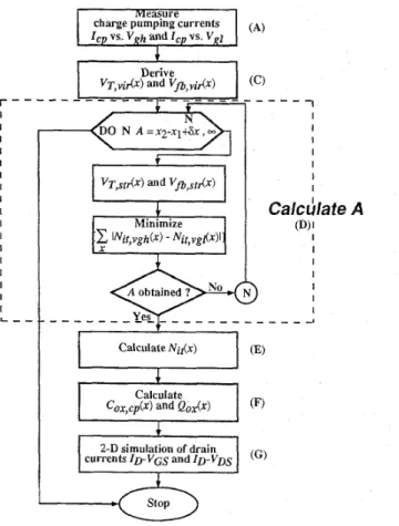
from the measured data. The goal of this work is to obtain these information with the aid of numerical calculations that can be easily programmed into an existing simulation framework, while with less measurement efforts. The extraction procedure used to characterize the damage profiles is shown by the flow diagram in Fig. 1. -1 I I I I I I I I I I- - - -
r - - - 6 I II
’
Fig. 1. Procedure of the proposed new technique to characterize N,+,(X)
and Qox(z). Inside each parentheses is the subsection character. Detailed descriptions will be presented in each of these subsections.
rithm. Step I : Step 2: Step 3: Step 4: Step 5:
There are five major steps involved in this extraction algo- Measure charge pumping currents I,, for the tested device before and after the stress.
Derive local threshold
V~,,,,..,,
and flatband volt- agesV&,vlr(x)
of fresh devices from the measured Icp’s before stress in Step 1.Determine the local threshold
V T , ~ ~ ~ ( Z )
(= V T , ~ ~ ~ ( ~ )+
AV*(.)) and flatband voltages Vfi,str(Z) (=V~I,,~~~(Z)
+
AVib(x)) of stressed devices from the measured Iccp’s in Step 1, and then determine the shifts of local threshold A&(.:) and flatband AV&,(x) voltages after the stress.Calculate N,t(x) and QOx(z) based on the results in Step 3 .
Compare the simulated I-V characteristics with the measurements after hot-carrier stress.
To illustrate this scheme, a step-by-step procedure will be described in more detail as follows.
A. Experimental Setup and Measured Charge Pumping Current
The basic setup for charge pumping measurement along with appropriate notations is shown schematically in Fig. 2. The gate of an LDD n-MOSFET device under test is connected to
Fig. 2. Basic experimental setup for charge pumping measurement, schematic diagram of an LDD MOSFET cross section and the corresponding notations.
a pulse generator (HP8 110A) while the drain and source are biased at ground voltage. Two kinds of 1-MHz pulse strings with rising/falling gradient of 25 n s N are used in our CP measurements [ 111. First, we use fixed base level, Vgl at -5 V, and sweep Vgh, then in the same way use fixed high level, Vgh at +5 V, and sweep Vgl (Vgh and Vgl are varied between -5 and +5 V) to measure CP currents for fresh (i.e., “virgin”) and
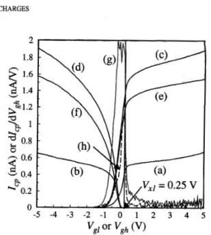
stressed LDD n-MOSFET’s. The CP currents were measured after a channel-hot-carrier stress at VGS = 3 V and VDS = 7 V for lo4 s. Fig. 3 shows the measured CP currents Icp
-
Vgh and Icp - Vgl for fresh and stressed devices. Since the local threshold voltage and local flatband voltage are not laterally uniform due to the variation of doping profile, for a certain Vgh (Vgl) value, only the interface states situated in the region, where the criteria of Vgh>
VT(z) and Vgl<
Vfi(z) are met as shown in Fig. 2, can be detected and contribute to charge pumping current. As a result, when Vgh (Vgl) exceeds the maximum (minimum) local threshold (flatband) voltage eventually, the whole detected region is covered, and then the I,, will become saturated at high Vgh ( Vgl) values.B. Formulation of IC, Versus Vgh or vgl Relationship Since the magnitude of I,, is a measure of the total amount
of interface states, based on [ 5 ] ,
[lo]
I,, versus Vgh curveafter the stress can be expressed by
(la) ~ 2 1.8
$
:::
-E: p . 2 % 1au
0.8-
0.63
0.4 3- + 0.28
n ” -5 -4 -3 -2 -1 0 1 2 3 4 5 Vglor
Vgh(V>
Fig. 3. (a) Icp versus Vgh (fresh), (b) Icp versus Vgl (fresh), (c) Icp versus Vgh (stressed), (d) Iccp versus vgl (stressed), (e) Icp,,j, versus V g h (stressed) and ( f ) Icp,,j versus V,, (stressed) curves of a W/Lm (= 20 pdO.7 p m ) LDD n-MOSFET’s with stress condition at V j s = 7 V and V& = 3 V,
measured at zero draidsource bias. (g) and (h) are the derivatives of curves (c) and (a), respectively.
Similarly, for the Icp versus Vgl relationship after the stress, we have
U [.
.
.] is a functionwith U defined by a step function
where
and
(3)
(4)
In (4) and (5), we make the implicit assumption that A v ~ ( x ) ( = VT+tr(z)
-
V T , ~ ~ ~ ( ~ ) ) at a position z along the channel is the same as AVfi(z)(= Vfi,str(z) - V i ~ , , ~ i ~ ( z ) ) during CP measurements. This can be justified from device54 IEEE TRANSACTIONS ON ELECTRON DEVICES, VOL. 43, NO. 1, JANUARY 1996
in the simulator and we see that A v ~ ( x ) and AVk,(x) are approximately equal. In addition, to first-order approximation the influence of NIt has the same effect on AV, and
AV,
(refer to Fig. 10 of [13]). From (1) and (2), we can see that there are two unknown variables Nit(x) and QOX(x) of interest in these two equations. Therefore, Nit(x) and Q O X ( x ) can be calculated numerically by solving the above two equations iteratively until the convergence is achieved. However, this self-consistent calculation for Nit (x) and Q,, (x) usually requires a huge computing time. For the purpose of easy computation, we use a very unique way to find the solutions in the following subsections.
C. Derivation of Local Threshold V T , ~ ~ ~ ( ~ ) and Flatband Vfi,vir(x) Voltages of Fresh Devices
By assuming symmetrically identical nature of the source and drain sides and the uniform interface state distribution for the tested devices before the stress, the local threshold
VT,vir(z)
and flatband Vfi,vir(x) voltages can be obtained from the CP currents Icp - vgh and Icp -
Vgl,
respectively, and represented by the following expressions [ 111:1) For the local threshold voltage V T , ~ ~ , ( ~ ) of fresh devices VT,vir(x) = Vgh
and
x(Vgh)=xLc+ (1- 'cp(Vgh)
)
.
(ZLd - Z L ~ ) . (6)Ic p ,vir, max
2) For the local flatband voltage V&ir(x) of fresh devices
and
.(Vgl) = X L C
+
'cp(vgl) ' (%Ad - x L c ) . (7)ICp,"lr,mE%X
Here, the channel end point on drain side XLd, that can be detected with charge pumping method, is determined by simulating the majority-carrier concentrations to define the effective channel length L,ff which contributes to the charge
pumping current [ 6 ] , [ 131, while the center point of the channel
x~~ depends on the gate mask length. In this case, MINIMOS 4 is used to calculate the majority-carrier distribution. The channel end point on drain side X L d was at 0 745 pm while
Vg, was held at -5 V. The center point of the channel X L ~ was 0.35 mm. From (6) and (7), we can directly obtain the local
threshold V T , ~ ~ ~ ( , ) and flatband Vfi,vir (x) voltage distributions of fresh devices as shown with solid lines along the channel in Fig. 4.
D. Determination of the Local Threshold V-,str(x) and Flatband V&tr (x) Voltages f o r Stressed Devices
First of all, we assume the two channel-hot-carrier induced VT,str(S) and V6,+tr(x), can be empirically formulated as (8) and (9), for the damaged region near the drain side, while
1 0 n -1
>
4s
-2 Ws"
-3 -4 -5Metallurgical junction1 Gate
r'
, , , , ~ , ,'I\0.5 0.55 0.6 0.65 0.7 0
Position
(pm)
Fig. 4.
along channel before and after the stress.
Local threshold VT(Z) and flatband & b ( z ) voltage distributions
VT,str(z) in the undamaged region remains unchanged as V T , ~ ~ ~ ( ~ ) (refer to Fig. 18 of [ll]). VT,str(X) = B . In (1 -
y )
+
VT,vir(xl) x15
x5
x2 0<
x<
x1 or 5 2<
x (8) where andVfi,str(x) = Vi,vir(x)
+
(VT,str(Z) - VT,vir(s)). (9) Here, x1 and 332 are the boundaries of the oxide damagedregion. In the above VT,str(x) formula, A is the only unknown variable to be determined. It should be noted that all the probable values of A are located between 2 2 - x1
+
Sx
and 00 (this can be seen from (8)). Fig. 5 shows the calculatedV T , ~ ~ ~ ( Z )
distributions from (8) with different values of A's for demonstration. In this figure, it illustrates that if theVT,str(z) curve is above the V,,,,,(,) curve, it corresponds to negative charges (electrons) being injected into the oxide which contributes to the rising of threshold and flatband voltages after the stress. In contrast, VT,+t,(x) below VT,,,,(,), shows the presence of positive charges (holes).
Before determining the value of A, we should first introduce
the derivation N,t,vgh(Z) and Nlt,vgh(x) from Icp - Vgh (i.e.,
from (1)) and Icp - Vgl (i.e., from (2)) curves, respectively, by assuming both V T , ~ ~ ~ ( X ) and V,,+tr(x) are given. A detailed
description of Nlt(x) (NItivgh(x) and Nlt,vgl(x)) derivation that incorporates the optimization technique is given in the Appendix.
Next, we want to determine the value of A in the following so that it can predict QOX(z) from VT,str(x) (i.e., Q o x ( x ) will
I
-2
0.5 0.55 0.6 0.65 0.7 0.75
Position
(pm)
Fig. 5.
for illustration. Here, VT,str(s) is empirically expressed by (8).
Calculated VT,str(s) distributions with various given values of A's
be determined whenever A is known). So far, there are still infinite probable sets of N i t , v g h ( X ) and Nit,vgl(z) in that A has not yet been determined. However, based on the fact that no test device has two different Nit(x) configurations at a certain point of time, we can confirm that, despite the errorshoise during measurements, Nit,vgh (z) should be completely the same as Nit,vgl(z) in principle. In numerical calculation, it means that the sum of differences between both Nit,vgh(x) and Nit,vgl(z), as derived in the Appendix, should be minimized (i.e., among all the probable A's, only one value, substituted into (A.l) and (A.2), can meet the criteria). Thus, the unique value A can be determined by minimizing the following
expression:
r 1
Here, we can easily use a DO-loop statement in the program to calculate the minimum of (lo), in which A is the DO
variable and the initial value is 2 2
-
z1+
Sz. It is noted that in principle the terminal value of A is 00 as describedpreviously. However, the terminal and increment values should be appropriately chosen, in such a way that A can be obtained
without difficulty. As long as A has been determined from the above algorithm, VT,str(Z) distribution can thus be obtained from (8). Results of VT,str(X) and V&tr(z) for stressed devices using the obtained A value are shown with dashed
lines in Fig. 4.
E. Determination of the Interjiace State Distribution
Once we have the values of VT,str(z), the coefficients of
To, T I ,
. .
.
T, in (A.6) can be calculated. Solving (A. 1 I), wecan obtain the solutions of ao, a l ,
. .
a,. Finally, the lateraldistribution of Ni,(z) can be determined by (A.3).
n
5
s"
1 0 -1 -2 -3 -4---
+1.10" cm-2-
fresh +5.10!! crt
0.6 0.65 0.7 0.75 0.8Position
(pm)
Fig. 6. Local threshold voltage distributions VT(I) (defined in [13]) with various uniform oxide charge profiles, simulated with MINIMOS 4. Significant differences in the shifts of V T ( Z ) inside and outside gate edge are observed.
F. Determination of the Fixed Oxide Charges by Incorporating 2 - 0 Fringing Effect
Usually, the ratio of AV,(.) and QOX(z) can be regarded as a linear constant Cox(= E ~ ~ / & , ~ ) , gate oxide capacitance
per unit area for convenience. This assumption holds only if the carriers injected into the oxide are strongly located under the gate channel region as in most conventional MOSFET cases. But for LDD or LDD-like MOSFET's, the vast majority of injected carriers reside beyond (or outside) the active channel region (especially, under the n- region). If we still use the constant Cox to calculate Qox(z) without considering
capacitive fringing effect for gate oxide [lo], Ell], this will induce serious errors due to the two-dimensional field induced fringing effect at the gate edge. To consider this 2-D effect, we may calculate a nonlinear capacitance Cox,cp (z) using device simulation. First, we calculate the local threshold voltage distributions as in Fig. 6 for several cases with given uniform
oxide charge distribution Qox covering electron and hole injections. Here, it can be seen that for the same amount of induced Q,,, AV,(z) is not a constant value, but depends on position (i.e.,
#
as shown in Fig. 6. m i l e without the 2-D effect, AV,, should be equal to AV,,). Given the above, Cox,cp(z) can be estimated according toThe value of Cox,cp(z) is maximum with Cox(=
~
~
in~
/
t
~
~
)
the middle of the gate and decreases gradually toward a much lower value outside the gate edge due to the fringing effect. The results are given in Fig. 7.
By incorporating this 2-D capacitive fringing effect, and then calculating the differences of local threshold voltage AVT(S) from Subsection 111-D, one can readily obtain the lateral distribution of oxide-trapped charges Qox (x) as follows:
86 IEEE TRANSACTIONS ON ELECTRON DEVICES, VOL. 43, NO. 1, JANUARY 1996 2 1 1
Gat5 edge
I
0.21
0 ~ ~ " ~ ' " ' ~ ~ " ~ ' ' " " ' 0.6 0.65 0.7 0.75 0.8 Position(pm)
Fig. 7.2-D fringing effect considered.
Calculated local gate-oxide capacitance Cox,cp (normalized) with
G. Ver$cation of the Drain Currents by Simulation
To verify the validity of the characterized Qox(z) and Nit(x), device simulator MINIMOS 4 has also been modified so as to incorporate nonuniform Q ox (x) and
Nit(x)
distribu- tions. In this simulation, the drain current characteristics ofI D - VGS, and I D - VDS both in normal and reverse modes are simulated and for comparison with experimental results.
Iv. RESULTS AND DISCUSSIONS
Usually, the range of hot-carrier-induced damaged region is about 0.2 pm and the damage profile is also well correlated with the lateral electric field peak as in [7]. Therefore, it should be noted that both x1 and x2 in (8) should be adequately
chosen. Here, we let 2 2 = x1;d = 0.745 pm (obtained in Section 111-G). As for 21, it is easy to infer from the principle of charge pumping that. the portion of the curves of the
dIc,,/dVgh characteristics before and after stress (curves g)
should coincide with each other and give the value Vzl, as
illustrated in Fig. 3. Thus, z1can be obtained by substituting
the value of V,, (as shown in the figure) into (6). In this case,
V,, = 0.25 V and 2 1 = 0.5 pm. Values of the optimized A and
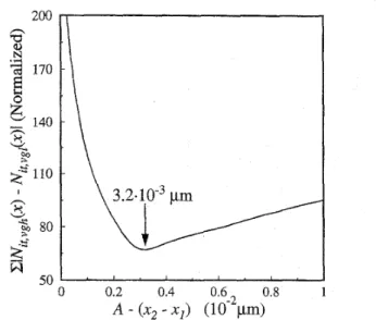
B are determined from (10). The result is illustrated in Fig. 8,
in which A - ( z ~ - z1) is 3.2 x pm. As soon as A is
determined, V T , ~ ~ ~ ( Z ) and flatband Vfi,str(z) can be calculated from (8) and (9) as shown in Fig. 4 for comparison. Fig. 9 shows the characterized spatial distributions of N;,(z) and
Q,,(z) from (A.3) and (12), respectively. Shown in the figure is also the lateral electric field which is peaked at the position close to the drain. It further shows that the lateral electric field is closely correlated with the oxide damaged region where Nit and Q,, are generated. By comparing the values of NI, and
Q o x , it shows that fixed-oxide charge effect is less pronounced
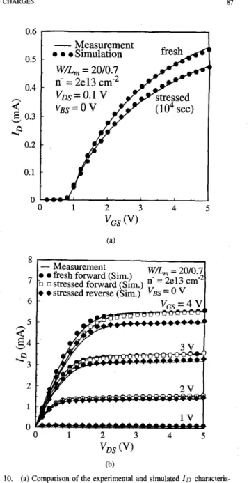
to the device degradation in LDD-type n-MOS devices. The simulated drain current characteristics I , - VGS and I D - VDS for both fresh and stressed devices are shown in
200 rl I
0 0.2 0.4 0.6-2 0.8 1
A - (x2 - X I >
(10
CL"
Fig. 8. Calculation of the minimum values of (10) for A .
Fig. 10(a) and (b), respectively. Comparison between simu- lation and experimental results shows very good agreements which also justifies the validity of the extracted NIt(z) and Qox(z) distributions.
The advantages of the present method are as follows:
1) In this experiment, we can easily obtain the lateral distributions of the induced NI, and Qox along the
channel merely from one set of CP currents, both
Icp
-
V,, and Icp - Vg, curves, measured at zerodraidsource bias. On one hand, because the drain and source are held constant at zero, this method can avoid the variations of V r ( z ) and
Vfi(z)
during the inversion and accumulation half cycles. On the other hand, it does not need multiple CP measurements, and hence avoids the likely imposition of re-stress on tested devices. 2) Since the variations of the induced Q,, are taken intoaccount in the calculation of NI, as in (1) and ( 2 ) , the inconsistency in determining the lateral position of the depletion edge [lo] can thus be eliminated in our new method.
3) By incorporating 2-D capacitive fringing effect (nonlin-
ear property of oxide capacitance) in calculating Q o x ( z ) ,
overestimation can be eliminated in that Cox is sig- nificantly larger Cox,cp (z), especially beyond the gate
edge.
4) The present method can be applied to LDD MOS devices without difficulty while most of the previous studies [7], [IO] are valid only for conventional MOS devices.
V. CONCLUSION
In this paper, the charge pumping technique has been successfully applied to the characterization of stressed n- channel LDD MOSFET devices. In particular, a new method has been developed for a consistent determination of the lateral distributions of both interface states and oxide-trapped charges.
LEE et al.: SPATIAL DISTRIBUTIONS OF INTERFACE STATES AND OXIDE-TRAPPED CHARGES 0.5 0.4 n
6
E
0.38
v 87 - - - 0.5 I i 500vn
0.4E
0 (U r(2
0.3 w W 0 1 ' '8028
2;"
0.1 n -0.1 0.2 0.3 0.4 0.5 0.6 0.7 0.8"Position
(pm)
Fig. 9. VDS = 7 V and VGS = 3 V.Lateral distributions of Nit(z), Q,,(z) and lateral electric field at
By incorporating the spatial distributions of Nit(") and QOX(z) into 2-D device simulator, predictions of I-V char-
acteristics for degraded devices can be accurately made. The simulation results have justified the validity of the proposed technique. It shows that our method can probe the hot-electron- induced oxide damage distribution with less measurements and greater precision. The developed result is expected to be useful for hot carrier reliability and performance studies of submicron or deep-submicron MOS devices.
APPENDIX
NUMERICAL SOLUTION OF INTERFACE STATES Nit (X)
In this appendix, we will describe the numerical solution of interface state distribution. By assuming that source and drain are symmetrical for fresh devices and damages are induced only near the drain side, the drain component Icp,d(= Icp (stressed) - Icp (fresh)/2) of CP current that flowing between drain and substrate can be shown as follows (from (3) and (4)): Icp,d(vgh) 4W.f / x L d Nit,vgh(x)U[Vgh - VT,str(x)]dx X L C (A. 1) and J X L C
To obtain the spatial profiles of Nit,vgh(Z) and Nit,vgI(x)
(we will concentrate on the derivation of Nit,vgh(x) in the
following. N i t , v g l ( ~ ) can be obtained in the same way) near
0.6
I
I 0.1 o.2I
-
Measurement
0 0 0Simulation
W/L,
= 20/0.7n'
=
2e
13 cm-2
P
I
I
6 5 W $4 3 2 1 bQFig. 10. (a) Comparison of the experimental and simulated I D characteris- tics for fresh and stressed devices. (b) Comparison of the experimental and simulated I o characteristics for fresh and stressed devices. The results for fresh characteristics are denoted by (e) and the results for stressed forward
(0) and reverse (4) characteristics are also shown.
the drain junction, we assume the functional relationship (n
can be chosen according to accuracy requirement)
with errors defined by (A.4), shown at the bottom of the page,
where Icp,d(Vgh) is the measured current at a specified Vg, and Nit,,,l(x) given by (A.3). We want to minimize the sum
88 IEEE TRANSACTIONS ON ELECTRON DEVICES, VOL. 43, NO. 1, JANUARY 1996 0.4 I 1 0.3
4-
5 0.2E!
2-
8
W c. 0.1- n = 3
- n = 4
- n = 5 -n=6 -n=7 - n = 8-n = 9
O L ' I " " " " Position(pm)
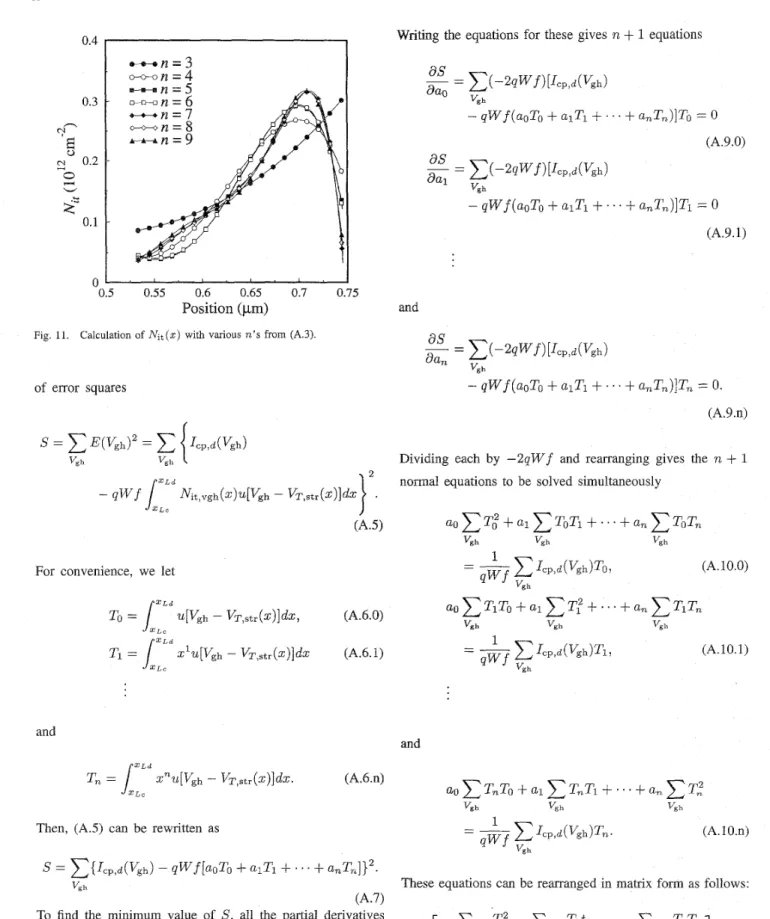
0.5 0.55 0.6 0.65 0.7 0.75Fig. 11. Calculation o f Nit (z) with various n's from (A.3).
of error squares
J X L C
For convenience, we let
(A.5)
(A.6.0)
(A.6.1)
Writing the equations for these gives n
+
1 equationsand
Dividing each by - 2 q W f and rearranging gives the n
+
1 normal equations to be solved simultaneouslyand
and (A.6.n)
Then, (AS) can be rewritten as
{ J c p , d ( V g h ) - qWf [aoTo
+
a1T1+
.
+
u ~ T , ] } ~ .v&
(A.7) To find the minimum value of S, all the partial derivatives should be zero, i.e.,
(A.lO.O)
(A. 10.1)
(A. 10.n)
I I
[13] P. Heremans, J. Witters, G. Groeseneken, and H. E. Maes, “Analysis of the charge pumping technique and its application for the evaluation of MOSFET degradation,” IEEE Trans. Electron Devices, vol. 36, p.
1318, 1989.
[I41 W. Chen and T.-P. Ma, “A new technique for measuring lateral dis- tribution of oxide charge and interface traps near MOSFET junctions,”
IEEE Electron Device Lett., vol. 12, p. 393, 1991.
(A. 1 1)
The solutions of the above equations gives uo, a1
,
u2,.
.
a,.Therefore, Ntt,+(x) can be calculated from (A.3). The com-
parison of calculated Nit for various n are shown in Fig. 11, in which n is chosen to be 7 for accuracy and numerical efficiency in this experiment.
Robert Giahn-Horng Lee was born in Taipei, Taiwan, Republic of China, in 1965. He received the B.S. degree in electrical engineering from Na- tional Cheng-Kung University, Taiwan, in 1987 and the M.S. degree in electronic engineering from National Chiao-Tung University, Taiwan, in 1992. He is currently working toward the Ph.D. degree at the Department of Electronic Engineering and Institute of Electronics, National Chiao-Tung Uni- versity. His current research interests include CMOS VLSIKJLSI technology, device design, device mod- REFERENCES
[I] K, R. Hofmann, C, werner, W. Weber, G, Dorda, “ ~ ~ ~ - ~ l ~ ~ ~ ~ ~ and hole-emission effects in short n-channel MOSFET’s,” IEEE Trans.
Electron Devices, vol. ED-32, p. 691, 1985.
[2] C. Hu, S. C. Tam, F. C. Hsu, P. K. KO, T. Y. Chan, and K. W. Tenill, “Hot-electron-induced MOSFET degradation-Model, monitor,
and improvement,” IEEE T ~~l~~~~~~ ~ D~ ~~ . ED-32, p, 375, ~ ~ ~ ~ ~ ,
1 a25
eling and simulation, and reliability study of miniaturized MOS devices.
Jen-Shien Su was born in Taiwan, Republic of China, in 1968. He received the B.S. degree in electrical engineering from Tatung Institute of Technology, Taiwan. in 1992 and the M.S. degree in electronic engineering from National K. K. Ng and G. W. Taylor, “Effects of hot-carrier trapping in n- and
p-channel MOSFET’s,” ZEEE Trans. Electron Devices, vol. ED-30, p.
871, 1983.
P. Heremans, R. Bellens, G. Groeseneken, and H. E. Maes, “Consistent model for the hot-carrier degradation in n-channel and p-channel MOSFET’s,” IEEE Trans. Electron Devices, vol. 35, p. 2194,
1988.
J. S. Brugler and P. G. A. Jespers, “Charge pumping in MOS devices,”
IEEE Trans. Electron Devices, vol. ED-16, p. 297, 1969.
G. Groeseneken, H. E. Maes, N. Bertran, and R. F. De Keersmaecker, “A reliable approach to charge-pumping measurements in MOS transistors,”
IEEE Trans. Electron Devices, vol. ED-31, p. 42, 1984.
M. G. Ancona, N. S. Saks, and D. McCarthy, “Lateral distribution of hot-carrier-induced interface traps in MOSFET’s,” IEEE Trans. Electron Devices, vol. 35, p. 2221, 1988.
B. Doyle, M. Bourcerie, J. C. Marchetaux, and A. Boudou, “Interface state creation and charge trapping in the medium-to-high gate voltage range ( & / 2 2 V, 2 v d ) during hot-camer stressing of n-MOS transistors,” IEEE Trans. Electron Devices, vol. 37, p. 744, 1990.
P. Habas and S. Selberherr, “A closed-loop extraction of the spatial distribution of interface traps based on numerical model of the charge- pumping experiment,” in Proc. Solid State Devices and Materials Con$,
1992, p. 170.
W. Chen, A. Balasinski, and T.-P. Ma, “Lateral profiling of oxide charge and interface traps near MOSFET junctions,” IEEE Trans. Electron Devices, vol. 40, p. 187, 1993.
M. Tsuchiaki, H. Hara, T. Morimoto, and H. Iwai, “A new charge pumping method for determining the spatial distribution of hot-carrier- induced fixed charge in p-MOSFET’s,” IEEE Trans. Electron Devices,
vol. 40, p. 1768, 1993.
A. B. M. Elliot, “The use of charge pumping currents to measure surface state densities in MOS transistors,” Solid-state Electron., vol. 19, p. 241,
1976.
U
.,
UChiao-Tung University, Taiwan, in 1994. His master thesis was on the characterization of hot carrier induced oxide damages in submicron MOS devices.
Steve S. Chung (S’83-M’85-SM’95) received the B.S. degree from the National Cheng-Kung Univer- sity, Taiwan, in 1973, the M.Sc. degree from the National Taiwan University, in 1975, and the Ph.D. degree from the University of Illinois at Urbana- Champaign, in 1985, all in electrical engineering.
From 1976 to 1978, he worked for an electronic instrument company as Head of the R&D division and subsequently as Manager of the Engineering Division. From 1978 to 1983, he was with the De- partment of Electronic Engineering and Technology at the National Taiwan Institute of Technology (NTIT) as a Lecturer. He was also in charge of an Instrument Calibration Center at NTIT. From 1983 to 1985, he held a research assistantship in the Solid State Electronics Laboratory and the Department of Electrical and Computer Engineering at the University of Illinois. In Sept 1985, he served at “T again as an Associate Professor in the Department of Electronic Engineering. Since August 1987, he has been
with the Department of Electronic Engineering and Institute of Electronics, National Chiao Tung University, Taiwan, and has been a Full Professor since the Fall of 1989. His current teaching and research interests are in the areas of solid-state device physics and VLSI technology; Spice device modeling; numerical simulation and modeling of submicron and deep-submcron MOS devices, SO1 devices, nonvolatile memories and TFT’s; characterization and reliability study of VLSI devices and circuits; and computational algorithms for VLSI circuits. He has authored and co-authored more than 60 international journal and conference papers in the above areas.
Dr. Chung has served as a Technical Program Committee Member of the ASIC Conference, IEEE, since 1989.
![Fig. 6. Local threshold voltage distributions VT(I) (defined in [13]) with various uniform oxide charge profiles, simulated with MINIMOS 4](https://thumb-ap.123doks.com/thumbv2/9libinfo/7690384.143264/5.921.76.430.121.411/threshold-voltage-distributions-defined-various-profiles-simulated-minimos.webp)