Photo-leakage-current characteristic of F incorporated hydrogenated amorphous
silicon thin film transistor
M. C. Wang, T. C. Chang, Po-Tsun Liu, S. W. Tsao, and J. R. Chen
Citation: Applied Physics Letters 90, 192114 (2007); doi: 10.1063/1.2738192 View online: http://dx.doi.org/10.1063/1.2738192
View Table of Contents: http://scitation.aip.org/content/aip/journal/apl/90/19?ver=pdfcov Published by the AIP Publishing
Articles you may be interested in
Suppression of Schottky leakage current in island-in amorphous silicon thin film transistors with the Cu Cu Mg as source/drain metal
Appl. Phys. Lett. 91, 062103 (2007); 10.1063/1.2767147
Direct-current substrate bias effects on amorphous silicon sputter-deposited films for thin film transistor fabrication
Appl. Phys. Lett. 87, 132108 (2005); 10.1063/1.2061860
Explanation for the leakage current in polycrystalline-silicon thin-film transistors made by Ni-silicide mediated crystallization
Appl. Phys. Lett. 81, 3404 (2002); 10.1063/1.1517406
Estimation of the impact of electrostatic discharge on density of states in hydrogenated amorphous silicon thin-film transistors
Appl. Phys. Lett. 80, 3337 (2002); 10.1063/1.1476394
Effect of Cl incorporation on the performance of amorphous silicon thin film transistors J. Appl. Phys. 82, 4081 (1997); 10.1063/1.366260
This article is copyrighted as indicated in the article. Reuse of AIP content is subject to the terms at: http://scitation.aip.org/termsconditions. Downloaded to IP: 140.113.38.11 On: Thu, 01 May 2014 00:29:18
Photo-leakage-current characteristic of F incorporated hydrogenated
amorphous silicon thin film transistor
M. C. Wang
Department of Materials Science and Engineering, National Tsing Hua University, Hsin-Chui 300, Taiwan T. C. Changa兲
Department of Physics, National Sun Yat-sen University, 70 Lien-hai Road, Kaohsiung 804, Taiwan and Institute of Electro-Optical Engineering, Center for Nanoscience and Nanotechnology, National Sun Yat-sen University, 70 Lien-hai Road, Kaohsiung 804, Taiwan
Po-Tsun Liu
Department of Photonics, National Chiao Tung University, Hsin-Chu 300, Taiwan and Display Institute, National Chiao Tung University, Hsin-Chu 300, Taiwan
S. W. Tsao
Institute of Electro-Optical Engineering, National Sun Yat-sen University, Kaohsiung 804, Taiwan J. R. Chen
Department of Materials Science and Engineering, National Tsing Hua University, Hsin-Chui 300, Taiwan 共Received 28 March 2007; accepted 18 April 2007; published online 10 May 2007兲
The photo-leakage-current共IPLC兲 characteristic of F incorporated a-Si:H thin film transistor 共TFT兲 has been studied. The device activation energy 共Ea兲 of a-Si:H共:F兲 TFTs is higher than those of
typical a-Si: H TFTs, and resulted in the shift down of Fermi level in a-Si: H共:F兲. Experimental results show that the IPLCof a-Si: H共:F兲 TFTs is smaller than that of conventional a-Si:H TFTs in
the density of states limited region, stemmed from the higher recombination centers present in
a-Si: H共:F兲 material. However, the higher IPLCis observed in the hole conduction region, resulted
from the larger Eain the a-Si: H共:F兲 TFTs. © 2007 American Institute of Physics.
关DOI:10.1063/1.2738192兴
Amorphous Si hydrogenated thin film transistors 共a-Si:H TFTs兲 have been widely used as switching devices for active matrix liquid crystal displays共LCDs兲. The a-Si:H TFT is particularly advantageous to the production of large flat panel displays and facilitates mass production.1,2Because
a-Si: H is a photosensitive material, the main objectives for
flat panel display application are to enhance the field effect mobility and to reduce the off-state leakage current under backlight illumination.3 The off-state leakage current under light illumination is, in particular, a serious problem in the projection and/or multimedia displays that require high in-tensity backlight illumination. In order to reduce the parasitic capacitance between the gate and source/drain electrodes, a self-aligned a-Si: H TFT structure has been proposed. How-ever, the higher off-state leakage current under light illumi-nation compared to a conventional TFT has been observed.4 As a result, the reduction of off-state photo-leakage-current in a-Si: H TFT is very important for TFT-LCDs technology. The most widely adopted method to lower the off-state photo-leakage-current is to reduce the thickness of undoped
a-Si: H layer. However, the reduced undoped a-Si: H
thick-ness would decrease the production yield of large size TFT-LCDs and also decrease the field effect mobility of the TFT devices.5 The off-state dark leakage current of a-Si: H TFT mainly originates from the photoinduced hole current at the interface between a-Si: H and gate SiN layers. In contrast, electrons are the majority carriers of off-state current for the
a-Si: H TFT under light illumination, since electron mobility
is much higher than that of hole.6Recently, Cl incorporated hydrogenated amorphous silicon a-Si: H共Cl兲 has been pre-pared by various deposition methods using SiH2Cl2mixtures to improve film quality,7stability8and deposition rate.9 Fur-thermore, the off-state photo-leakage-current of a-Si: H TFT is also suppressed by the addition of Cl.10,11 The photo-leakage-current of a-Si: H共Cl兲 TFTs is at least two orders of magnitude lower than that of conventional a-Si: H TFTs,12 stemmed from the exhibited p-type-like behavior of
a-Si: H共:Cl兲 channel. Although the lower density of states
共DOS兲 by the addition of moderate F in a-Si:H was reported by Hyun et al.,13 the different results were observed in this letter. In this study, the a-Si: H共F兲 TFT with F incorporated active layer has been fabricated by using 6% SiF4into silane
plasma. The concentration of fluorine in the a-Si: H共F兲 active layer is about 4.970⫻1018at./ cm3 via the secondary ion
mass spectrometer analysis. The off-state leakage current characteristics of a-Si: H共:F兲 TFTs under light illumination was also investigated.
Inverted-staggered a-Si: H TFTs with back-channel-etched共BCE兲 process were fabricated on glass substrate for the study of electrical characteristics, as shown in the inset of Fig.1. The device fabrication process was described as fol-lows. After a 3000 Å thick Cr gate electrode was patterned on the glass substrate, a 3000 Å thick silicon nitride共SiNx兲
layer, a 2000 Å thick a-Si: H共:F兲 active layer, and a 500 Å thick n+-a-Si: H were continuously deposited by plasma en-hanced chemical vapor deposition method. The undoped
a-Si: H共:F兲 was deposited with a gas mixture of 3 SCCM
共SCCM denotes cubic centimeter per minute at STP兲 SiF4
and 50 SCCM SiH4 at 200 ° C. The n+-a-Si: H layer in the
a兲Author to whom correspondence should be addressed; FAX: 886-3-5722715; electronic mail: [email protected]
APPLIED PHYSICS LETTERS 90, 192114共2007兲
0003-6951/2007/90共19兲/192114/3/$23.00 90, 192114-1 © 2007 American Institute of Physics
This article is copyrighted as indicated in the article. Reuse of AIP content is subject to the terms at: http://scitation.aip.org/termsconditions. Downloaded to IP: 140.113.38.11 On: Thu, 01 May 2014 00:29:18
TFT channel region would to be etched off using the source/ drain pattern as a mask, after the electrodes are formed for TFTs. In order to decrease the device degradation of
a-Si: H共:F兲 layer, the a-Si:H/a-Si:H共F兲 double channel
layer structure was also fabricated for this study. The thick-nesses of a-Si: H and a-Si: H共F兲 in double layer structure were 40 and 160 nm, respectively. The channel length of TFT devices varied from 5 to 16m and the channel width was kept constant 24m. Similarly, the conventional
a-Si: H TFTs without gas mixture of SiF4 were also
fabri-cated as a reference sample. The photo-leakage-current mea-surement was carried by light illumination from the back side of substrate to compare the difference in the off-state photo-leakage-currents between the a-Si: H共:F兲 TFT and the conventional one. The intensity of cold cathode fluorescent lamp backlight source was fixed at 3300 cd/ m2.
After a complete TFT manufacture process, the charac-teristics of the a-Si: H TFT demonstrated the field effect mo-bility ranging from 0.43 to 0.64 cm2/ V s, the minimum sub-threshold swing from 0.58 to 0.59 V / decade, and the Ion/ Ioff
ratio is 106 at V
D= 10 V. The threshold voltage was
distrib-uted from 2.02 to 2.08 V, determined from turn-on current 共Ion兲 extrapolation in the linear region of ID-VGcurve at VD
= 0.1 V. The a-Si: H共:F兲 TFT demonstrated the field effect mobility from 0.35 to 0.58 cm2/ V s, the minimum sub-threshold swing from 0.65 to 0.67 V / decade, and the thresh-old voltage from 2.57 to 3.99 V. In contrast, the double channel layer TFT demonstrated the field effect mobility from 0.38 to 0.60 cm2/ V s, the minimum subthreshold
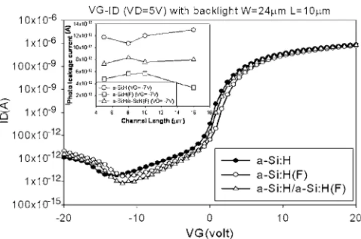
swing from 0.59 to 0.62 V / decade, and the threshold volt-age from 2.14 to 2.36 V. Figure2shows the comparison of the transfer characteristics between a-Si: H, a-Si: H共:F兲, and double channel layer TFTs under backlight illumination. As shown in the comparison, the off-state photo-leakage-currents of a-Si: H共:F兲 TFTs and double channel layer TFTs are smaller than those of conventional a-Si: H TFTs in the DOS limited region. It is also because the a-Si: H TFT under backlight illumination was in the nonequilibrium state 共pn ⬎ni
2兲. As a result, the trap states played the role of
recombi-nation centers. The photo-leakage-current of a-Si: H共:F兲 TFT operated in the small negative gate voltage共VG⬎−10 V兲 and
5 V drain voltage is less than 60% of conventional a-Si: H TFTs. Because the electric field is not large enough to
sepa-rate the photoinduced electron-hole pairs, the increased density of states serving as recombination centers in
a-Si: H共:F兲 channel material has resulted in the lower
photo-leakage-current. However, with the hole conduction region 共VG⬍−10 V兲, the larger photo-leakage-current was
ob-served. According to previous study,6 the larger off-state photo-leakage-current is due to the faster hole channel accu-mulation in the larger negative gate voltage. The smaller hole accumulated voltage also indicated that the undoped
a-Si: H共:F兲 shows near p-type-like behavior. Typical a-Si:H
is n-type material even though the Fermi level lies near the midgap of undoped a-Si: H because the electron mobility is at least ten times higher than that of hole.6 The undoped
a-Si: H共:F兲 TFTs have shown larger threshold voltage and
smaller field effect mobility. The double channel layer TFTs also indicated that the lower photo-leakage-current was not simply resulted from the shift of threshold voltage. A reason-able explanation is the shift of the Fermi level toward the valence band. The increase in the threshold voltage may originate from the increase of the defect density by F incor-poration and lead to a resultant Fermi level shift toward the valence band edge.6The Fermi level of a-Si: H is determined from the charge neutrality condition. Some trap states within the band gap are charged positively and other states are nega-tively charged by the same amount. The a-Si: H共F兲 TFT with F incorporation has shown the larger threshold voltage and lower field mobility than conventional counterpart. In order to make sure the increase of acceptorlike state in a-Si: H共F兲 channel material, the activation energies共Ea兲 of a-Si:H共F兲
TFTs and conventional a-Si: H TFTs were extracted from varied temperature measurement in the temperature range from room temperature to 125 ° C.14,15As shown in Fig. 3, the Ea of the a-Si: H共F兲 and double channel layer TFTs are
larger than conventional a-Si: H TFTs. At VG= 0 V, the
Fermi level EF of a-Si: H TFT is situated below about
0.49 eV from the conduction band edge EC. However, the
Fermi level EF of a-Si: H共F兲 TFT is situated below about
0.63 eV from the conduction band edge EC. The Fermi level EF of double channel layer structure TFT is situated below about 0.82 eV. This value indicates that in a-Si: H共F兲 chan-nel, the density of the donorlike defect states is reduced than the density of the acceptorlike defect states. Also, the
a-Si: H共F兲 TFT behaves as a similar p-type property com-FIG. 1. Dark transfer characteristics of a-Si: H, a-Si: H共F兲 TFTs, and double
channel layer structure TFTs. The inset shows the structure of BCE inverted-staggered TFT devices with a-Si: H, a-Si: H共F兲, and double channel layer.
FIG. 2. Comparison of transfer characteristics between a-Si: H, a-Si: H共:F兲 TFTs, and double channel layer TFTs under light illumination. The inset shows the magnitude of photo-leakage-current at VG= −7 V with different
channel lengths.
192114-2 Wang et al. Appl. Phys. Lett. 90, 192114共2007兲
This article is copyrighted as indicated in the article. Reuse of AIP content is subject to the terms at: http://scitation.aip.org/termsconditions. Downloaded to IP: 140.113.38.11 On: Thu, 01 May 2014 00:29:18
pared with the a-Si: H TFT and results in the little electrical degradation with F incorporation. The correlation between the DOS and the gate voltage allows obtaining the distribu-tion of the density of states by studying the dependence of Ea
vs VG. Globus et al.16proposed a method to evaluate DOS in a-Si: H TFTs through the dependence of Eavs VG.
The distribution of density of states g共Ea兲 was estimated
from Fig.3with the slope of Ea− VGcurve. The acceptorlike
states are nearly about 5⫻1016 and 1⫻1017cm−3eV−1 for
both the a-Si: H and the double channel layer TFT. Further-more, the Fermi level is shifted through these states during the operation of TFT devices in the subthreshold region. The additional deep states have been found in the a-Si: H共F兲 TFT and the double channel layer TFTs. These additional deep states in a-Si: H共F兲 TFT thereby resulted in lower photo-leakage-current compared to the a-Si: H TFT, and illustrated by the inset of Fig.3. The double channel layer TFTs have shown the less degradation on device characteristics. These results also indicated the slight degradation on a-Si: H共F兲 TFT. The increase of acceptorlike deep state in a-Si: H共F兲 material leads to slight electrical degradation on a-Si: H共F兲 TFTs and results in the shift down of Fermi level.
We have fabricated a-Si: H共F兲 and the double channel layer TFTs in which the a-Si: H共F兲 layer was deposited with the ratio of 6% SiF4into silane plasma. The a-Si: H共F兲 TFTs
have shown the better characteristic against photoillumina-tion, resulted from the increase of acceptorlike deep states in
a-Si: H共F兲 material. The double channel layer TFTs have
shown the less degradation on device characteristic and the lower photo-leakage-current. The incorporation of F in
a-Si: H channel material, however, appears to shift the Fermi
level toward the valence band edge due to the increase of acceptorlike deep states in a-Si: H共F兲 material. This makes the a-Si: H共F兲 TFT trend to p-type conduction. Since a smaller voltage is required for hole accumulation, the larger photo-leakage-current is observed with the increase of nega-tive VG. These results indicated that a-Si: H TFT with F
dop-ing could reduce the photo-leakage-current 共VG⬎−10 V兲
due to the increase of acceptorlike deep states as recombina-tion centers in a-Si: H共F兲 material.
This work was partially supported by National Science Council, the Republic of China under Contract Nos. NSC-95-2120-M-110-003, NSC94-2215-E-009-031, NSC95-2221-E-009-254-MY2, and MOEA Technology Develop-ment for Academia under Project No. 94-EC-17-A-07-S1-046 and MOE ATU Program. Also, the authors thank the support from AU Optronics Corp.共AUO兲, Taiwan.
1F. B. Ellis, Jr., R. G. Gordon, W. Paul, and B. G. Yacobi, J. Appl. Phys.
55, 4309共1984兲.
2R. Baeuerle, J. Baumbach, E. Lueder, and J. Siegordner, SID ’99 Digest, Society of Information Display, 1999共unpublished兲, p. 14.
3J. K. Yoon, Y. H. Jang, B. K. Kim, H. S. Choi, B. C. Ahn, and C. Lee, J. Non-Cryst. Solids 164–166, 747共1993兲.
4M. Akiyama, T. Kiyota, Y. Ikeda, T. Koizumi, M. Ikeda, and K. Suzuki, SID ’95 Digest, Society for Information Display, Florida, 1995 共unpub-lished兲, p. 158.
5N. Hirano, N. Ikeda, H. Yamaguchi, S. Nishida, Y. Hirai, and S. Kaneko, IDRC ’94 Digest, International Display Research Conference, CA, 1994 共unpublished兲, p. 369.
6W. E. Spear, J. Non-Cryst. Solids 59/60, 1共1983兲.
7J. N. Bullock and S. Wagner, Mater. Res. Soc. Symp. Proc. 336, 97 共1994兲.
8T. Oshima, K. Tamaguchi, A. Yamada, M. Koganai, and K. Takahashi, Mater. Res. Soc. Symp. Proc. 336, 91共1994兲.
9M. Nakata and S. Wagner, Appl. Phys. Lett. 65, 1940共1991兲.
10J. S. Byun, H. B. Jeon, K. H. Lee, and J. Jang, Appl. Phys. Lett. 67, 3786 共1995兲.
11K. S. Lee, J. H. Choi, S. K. Kim, H. B. Jeon, and J. Jang, Appl. Phys. Lett.
69, 2403共1996兲.
12J. H. Choi, C. S. Kim, S. K. Kim, and J. Jang, J. Appl. Phys. 82, 4081 共1997兲.
13C. H. Hyun, M. S. Shur, and A. Madan, Appl. Phys. Lett. 41, 178共1982兲. 14R. E. I. Schropp, J. Snijder, and J. F. Verwey, J. Appl. Phys. 60, 643
共1986兲.
15R. Schumacher, P. Thomas, K. Weber, W. Fuhs, F. Djamdji, P. G. Le Comber, and R. E. I. Schropp, Philos. Mag. B 58, 389共1988兲. 16T. Globus, H. C. Slade, M. S. Shur, and M. Hack, Mater. Res. Soc. Symp.
Proc. 336, 823共1994兲. FIG. 3. Extracted activation energy Eafor the a-Si: H共F兲 TFT and
conven-tional a-Si: H TFT. The inset shows the mechanism of DOS as recombina-tion centers under backlight illuminarecombina-tion.
192114-3 Wang et al. Appl. Phys. Lett. 90, 192114共2007兲
This article is copyrighted as indicated in the article. Reuse of AIP content is subject to the terms at: http://scitation.aip.org/termsconditions. Downloaded to IP: 140.113.38.11 On: Thu, 01 May 2014 00:29:18