photoluminescence of ZnO quantum dots–SiO
xN
ynanocomposite films
Yu-Yun Peng and Tsung-Eong Hsieha)
Department of Materials Science and Engineering, National Chiao Tung University, Hsinchu, Taiwan 300, Republic of China
Chia-Hung Hsu
Research Division, National Synchrotron Radiation Research Center (NSRRC), Hsinchu, Taiwan 300, Republic of China
(Received 3 September 2007; accepted 15 January 2008)
Nanocomposite films containing ZnO quantum dots (QDs) and SiOxNy matrix were
prepared by target-attached radio frequency sputtering. Photoluminescence (PL) dominated by violet and blue emissions was observed from all ZnO QD–SiOxNy
nanocomposite films with dot diameters ranging from 2.77 to 6.65 nm. X-ray photoemission spectroscopy (XPS) revealed the formation of nitrogen-correlated bonding configurations in both the SiOxNymatrix and the dot/matrix interfaces. The
nitrogen-correlated configuration at the interface produced a substantial polarization effect at dot surface. The suppression of green-yellow emission observed in
photoluminescence spectra of all samples was ascribed to the hole-trapping process promoted by the enhancement of the surface polarization.
I. INTRODUCTION
Recently, semiconductor quantum dots (QDs) embed-ded in various dielectric materials have attracted consid-erable research interest. Apart from quantum confine-ment due to the nanometer dimension,1 semiconductor QDs embedded in a dielectric material experience spe-cific effects such as dielectric confinement2–7and surface polarization at the surface of QDs.8–10The influences of dielectric environment on optical properties of nano-structured semiconductors have been discussed.11–13 Implanting nanostructured semiconductors into specific dielectrics produces composite materials with unique lu-minescence properties; their applications to optoelec-tronic devices and biosensors have been demonstrated. For instance, the CdSe-dielectric system may serve as an active medium in tunable lasers to achieve full-color emission.14,15
Similar to CdSe-dielectric systems, ZnO-dielectric systems with distinct luminescent properties have been developed.16–19One advantage of the ZnO-dielectric sys-tems is that it does not suffer severe oxidation and deg-radation as in the CdSe-dielectric system. Moreover, the wide band gap (Eg⳱ 3.25 to 3.5 eV) and large exciton
binding energy (59 meV) of ZnO allow ZnO-dielectric systems to exhibit a high luminescence efficiency at room temperature. At present, the ZnO–SiO2composite prevails over other ZnO-dielectric systems because it can be prepared through several methods, such as sol-gel,20,21 molecular capping,22 impregnation method,23 etc. In previous studies, we prepared the ZnO QDs–SiO2 nanocomposite films with dot diameters ranging from 1.96 to 6.54 nm by a target-attached sputtering method.24,25 Gaussian curve fitting of photolumines-cence (PL) spectra showed that the integrated intensities of three emission bands from ZnO QDs–SiO2 nanocom-posite films vary with the surface-to-volume ratio (SV ratio) of QDs. An analysis of luminescent intensity in relation to defect energy levels indicated that the mecha-nisms of emission transitions are strongly affected by the presence of ZnO/SiO2interfaces. Consequently, we pre-pared ZnO QDs–SiOxNynanocomposite films and
inves-tigated their luminescent properties and microstructures to explore the effects of dielectric matrix type on the photoemission mechanisms of ZnO QD. Our analysis of the photoelectron signals reveals the chemical bonding structures in these nanocomposite samples and derives specific bonding configurations correlating to nitrogen at the ZnO QDs–SiOxNy interface. The incorporation of nitrogen atoms at the dot/matrix interface and its influ-ence on the luminescent properties of ZnO QDs–SiOxNy nanocomposite films are also discussed.
a)
Address all correspondence to this author. e-mail: [email protected] DOI: 10.1557/JMR.2008.0134
II. EXPERIMENTAL DETAILS
The ZnO–SiOxNy nanocomposite films containing ZnO QDs with diameters ranging from 2.77 to 6.65 nm were fabricated by target-attached sputtering. The samples were prepared by attaching ZnO (99.999%) pel-lets in adequate area proportions on a Si3N4 (99.5%,
51 mm) target during sputtering deposition under these conditions: radio frequency (rf) power, 50–200 W; flow-ing gas, Ar + 2.5% N2; working pressure, 3–10 mTorr. Si
wafers were adopted as substrates; neither substrate heat-ing nor postannealheat-ing was performed. As the Si in Si3N4
can combine with O− or O2−from ZnO pellets or from residual CO3
2−
in the vacuum chamber to produce SiOx during sputtering, the dielectric matrix of the nanocom-posite films is thus metastable SiOxNy instead of pure Si3N4.
The microstructure of the samples was characterized with a transmission electron microscope (TEM; Philips TECNAI 20 FEG) (Eindhoven, The Netherlands). The chemical bonding was examined with x-ray photoemis-sion spectroscopy (XPS) recorded with a Mg K␣source (American Physical Electronics ESCA PHI 1600) (Chanhassen, MN). The PL spectra were measured at room temperature using a He–Cd laser with emitting wavelength of 325 nm.
III. RESULTS AND DISCUSSION
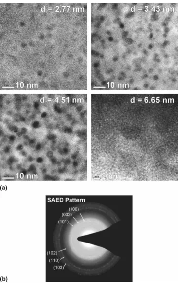
A. Microstructure of ZnO–SiOxNynanocomposites Figure 1(a) shows the TEM micrographs of ZnO QDs– SiOxNy nanocomposite films containing ZnO QDs of various sizes. The density of ZnO QDs increases as the dot size increases from 2.77 to 6.65 nm. A typical se-lected-area electron diffraction (SAED) pattern of nanocomposite film presented in Fig. 1(b) indicates that the nanoscale ZnO QDs are crystalline25 rather than amorphous clusters. TEM characterization also revealed that, though the ZnO QDs–SiOxNy and ZnO QDs–SiO2
systems possess similar microstructures, the thermal sta-bility of SiOxNy matrix seems inferior to that of SiO2
matrix. During electron bombardment, the ZnO QDs– SiOxNy films were prone to break, and pores developed in TEM samples. This is attributed to the absorption of thermal energy by dangling bonds in the SiOxNymatrix which, in turn, results in the contraction of samples.
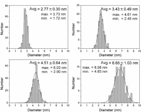
Figure 2 displays the histograms of ZnO dot size de-duced from the TEM characterizations on the samples shown in Fig. 1(a). The sizes of over 80 ZnO dots were measured in each sample, and the distribution was fitted by a Gaussian function. It was found that the samples with small dot sizes and low dot densities contained well-separated ZnO QDs with narrow distributions of size. For samples with large dot sizes and high dot densities, neighboring ZnO dots tended to coalesce and become large crystalline clusters.
B. PL spectra and Gaussian curve fittings
PL spectra of ZnO QDs–SiOxNynanocomposite films are shown in Fig. 3(a). There is no significant variation of the shape of spectra for all samples, but the luminescence intensities vary with dot sizes. The green-yellow emis-sions in the ZnO QDs–SiOxNy system are less intense than those observed in the ZnO QDs–SiO2 system,
24,25
even for those samples with severe coalescence of dots. The green-yellow emission is attributed to VO⭈/VO⭈⭈
resid-ing in the bulk region of QD, whereas the violet and blue emissions are related to surface states or VZnacceptors at
the dot surface.24,25
In contrast to ZnO QDs–SiO2
films,24,25
there is no extra or absent emission in the PL spectra of ZnO QDs–SiOxNy films, implying that the change of dielectric matrix type creates no new defect species in ZnO QD.
The optimized Gaussian curve fitting of PL spec-tra was performed under the consspec-traint wviolet ≈ wblue
FIG. 1. (a) TEM images of ZnO QDs–SiOxNynanocomposite films
containing ZnO QDs with dot diameters ranging from 2.77 to 6.65 nm. (b) A typical SAED pattern of ZnO QDs–SiOxNynanocomposite films
containing.
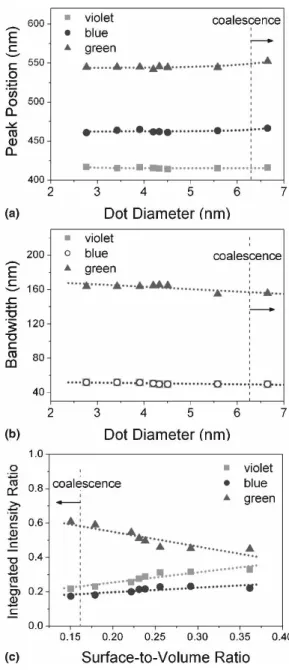
(w⳱ bandwidth of emission band). As illustrated in Fig. 3(b), the spectrum contains three emission bands, i.e., violet, blue, and green-yellow bands, with corresponding photon energies about 2.98, 2.66, and 2.28 eV, respec-tively. The peak position and bandwidth of each emission versus the dot diameter deduced from the curve fitting of PL spectra are presented in Figs. 4(a) and 4(b). These interband transitions of ZnO QDs–SiOxNy films exhibit no significant blue shift as the dot size decreases. We speculated that these defect levels or trap states might be affected or pinned by the surface/interface bonding con-figurations, especially for small dots, and result in a band shift behavior of the interband transition dissimilar to that of a near-band-edge transition.25The dependence of integrated intensity of the violet and blue emissions on the SV ratio are shown in Fig. 4(c). It can be seen that the integrated intensities of the green-yellow emission for ZnO QDs–SiOxNy films are smaller than that for the
ZnO QDs–SiO2 films. 24,25
Such a distinct variation can be seen by comparing the peak intensities of the two nanocomposite systems. For ZnO QDs–SiOxNyfilm with dot diameter of 2.77 nm, the peak intensity of the violet emission is about 2.3 times that of the green-yellow emission, while for ZnO QDs-SiO2film with a
compa-rable dot size, the peak intensities of the two peaks are nearly the same.
C. XPS analysis of the bonding characteristics of nanocomposite samples
The chemical compositions of a ZnO QDs–SiOxNy nanocomposite films were identified with the aid of XPS FIG. 3. (a) PL spectra of ZnO QDs–SiOxNynanocomposite films with
dot diameters ranging from 2.77 to 6.65 nm. (b) An example of Gauss-ian curve fitting of PL spectra consisting of violet, blue, and green-yellow emission bands.
analysis. According to XPS data, the binding energy (Eb)
of Zn 2p3/2 (1022.20 ± 0.10 eV) in ZnO QDs–SiOxNy (not shown) is identical to that observed in the ZnO QDs–SiO2system, implying a formation of the Zn
2+
va-lence state in oxygen-deficient ZnO1−x.
26
The photo-emissions corresponding to Si, N, and O atomic levels are, however, rather complicated because of the presence of oxygen-containing ZnO and SiOxNy matrix in which the SiOxNymatrix might contain more than one chemical component, as described below.
An analysis of the O 1s atomic level in ZnO has been reported elsewhere.24Two oxygen species are present in ZnO27: the lattice oxygen Olattice(O1) denoted by O
2−
in
the crystalline network (530.1–530.4 eV), and O− ions (O2) residing at sites at which the coordination number of oxygen ions is smaller than that at a regular site, e.g., subsurface (531.2–531.7 eV). Investigations of O 1s atomic level in SiOxNymatrix (O3) by characterizing the allotropes with various chemical stoichiometries have been reported previously.28–33
Major differences be-tween the photoemission signals of SiOxNy glass was ascribed to the varied bonding structures of basic units. In SiOxNyglass, the atomic configuration might contain oxygen-bridged (SiO4)-structural units, tetrahedral
(SiN4)-units linked by a nitrogen atom, and their
com-plexes.29–33 Generally, a Si 2p atomic level in SiOxNy (Si1) has Eblying in between the values for pure Si3N4
and for pure SiO2(Si2), i.e., 101.7–103.3 eV, whereas Eb
of O 1s in SiOxNy(O3) shifts slightly to values less than that in SiOxdue to the competition of the electron affinity with the nitrogen atom. Eb of N 1s exhibits a strong
dependence on chemical stoichiometry that corresponds to the combinations with varied amounts or types of atomic bonding. The N–Si3/N–(SiOx)3 (N1) and Si2–
N–O (N2) exhibit distinct binding energies because of a severe chemical shift (1.7–2.0 eV) by the presence of the N–O bond.29–33 Table I summarizes the Eb of Si 2p,
N 1s, and O 1s with the correlated atomic bonding in the ZnO QDs–SiOxNy system.
The XPS curves were analyzed (curve fitting program XPSPEAK 4.1) with a combination of Gaussian (80%) and Lorentzian (20%) distributions. Figures 5(a), 5(b), and 5(c) show the XPS features of Si 2p, N 1s, and O 1s atomic levels, respectively. The Si 2p spectra have two components: Si1 represents the (SiO4)-units and Si2
originates from the SiOxNy-like component. Figure 5 in-dicates that there are fewer pure (SiN4)-units (∼101.7 eV)
in samples because of the large population of O atoms. Hence the (SiO4)-units decrease as the Si content
de-creases, implying that the matrix prefers the SiO2–
SiOxNystate at a high Si content (i.e., low proportion of ZnO) and switches to the SiOxNystate at a low Si content (i.e., high proportion of ZnO). The variation between the two nitrogen components (N1 and N2) as the Si content decreases can be readily seen in the fitted spectra [Fig. 5(b)] with an increasing tendency of the atomic combi-nation from an N–Si bond to an N–O bond. A small TABLE I. Summary of binding energies of Si 2p, N 1s, and O 1s atomic levels in ZnO26,27and SiO
xNymaterials.
28–33
Materials
Binding energy, Eb(eV)
Si 2p N 1s O 1s
ZnO ⭈⭈⭈ ⭈⭈⭈ 530.0–530.4 (O1)
531.1–531.7 (O2)
Si3N4 101.7 397.4 ⭈⭈⭈
SiOxNy 101.7–103.3 (Si1) 397.4–398.4 (N1) 532.0–534.3 (O3) 399.0–401.0 (N2)
SiO2 103.3 (Si2) ⭈⭈⭈ 532.5–534.3
FIG. 4. Plots of (a) peak position and (b) bandwidth versus dot diam-eter and (c) integrated intensity ratio of emission band versus surface-to-volume ratio (SV ratio) deduced from the Gaussian curve fitting of PL spectra.
reduction of the O3 component relative to the O2 com-ponent is revealed by Fig. 5(c), and the Ebs also slightly
decrease as a result of the increasing N–O bonds. In consequence, oxygen atoms are allowed to form O–Si bonds in the samples with high Si content, whereas at low Si content, nitrogen atoms are prone to form N–O bonds with the loosely bound oxygen species in the samples.
The bonding state of ZnO was also characterized by analyzing the Auger Zn L3M4,5M4,5spectra as they are
more sensitive to the variation of the chemical environ-ment than the Zn 2p spectra. Figure 5(d) shows Auger Zn L3M4,5M4,5 spectra of ZnO QDs–SiOxNy films. In all samples, the Auger peaks at about 988.1 eV clearly re-veal the presence of Zn–O bonds in the oxide state. Moreover, the absence of Zn–N bonds34,35in the spectra indicates no nitrogen-doping in ZnO QD, even with the introduction of nitrogen gas flowing during sputtering. Thus the suppression of the green-yellow emission was
not originated from the p-type doping of ZnO; i.e., no shallow acceptor NO formed in ZnO QDs embedded in
the SiOxNymatrix.
36,37
D. N-correlated bonding configuration at the dot/matrix interface
Theoretical calculations showed that the N1 compo-nent possesses a binding energy shift (+0.19 to +0.66 eV) relative to interfacial N atoms in the N–Si3configuration
due to the presence of N atoms in the SiO2matrix [i.e.,
the formation of N–[Si(O–)3]3 configuration]. 38,39
Ac-cording to this finding, two bonding components, N1 and N2, in the ZnO QDs–SiOxNy system were obtained by fitting the N 1s XPS spectra. Figure 5(b) reveals that, as the dot size and density increase (i.e., when the Si content decreases), the N1 component decreases, whereas the N2 component increases. In contrast, the trend of the increas-ing N2 component indicates a distinct chemical bondincreas-ing configuration in the nanocomposite samples. In addition FIG. 5. Analytical results of XPS spectra for (a) Si 2p, (b) N 1s, and (c) O 1s atomic levels of ZnO QDs–SiOxNynanocomposite films. (d) Auger
to an influence of the processing temperature,32the for-mation of the N2 component is specifically related to the interfacial region.30,32,33Kobayashi et al.32reported that the processing temperature affects both the activities of ionic bonding and the stoichiometry of the SiOxNy ma-trix, which, in turn, alters the proportion of the N2 com-ponent. During our sputtering deposition, there was no significant substrate temperature variation; the increase of the N2 component with increasing dot size and density was thus not induced by thermal effects. The incorpora-tion of nitrogen atoms at the surface/interface was com-monly observed in the nitridation of SiO2because of the
smaller activation energy at the surface/interface re-gion.30,32,33 We thus speculated that the N2 component resides at the dot/matrix interfaces rather than in the ma-trix.
An incorporation of nitrogen atoms at the dot/matrix interface is also explicable through the large population of dangling O-bonds at the dot/matrix interface. Such dangling O-bonds are commonly observed at the SiO2/Si
interface that provides adsorption sites for certain species to be weakly bound. In the ZnO QDs–SiOxNysystem, the O− ions at the dot surface serve as dangling O-bonds, which attract nitrogen atoms to form N–O bonds or the N2 configuration. The formation of such a nitrogen-correlated configuration is also promoted by the active N+/N+2-plasma
31,32
generated by the introduction of ni-trogen gas during sputtering as the N+/N+2 species are
readily attracted to O−ions at the ZnO QD surface and induce the Si2–N–O bonding.
E. Effects of surface polarization on photoemission property
Considering the analytical results described above, we propose a surface bonding configuration model for the ZnO QDs–SiOxNysystem, as illustrated in Fig. 6(a). In Fig. 6(a), the O−ion residing at the dot surface27might interact with the N2 component of the SiOxNymatrix to form an O(␦−)–N(␦+) bond. Figure 6(b) presents the sur-face bonding configuration model of the ZnO QDs–SiO2
system for the purpose of comparison. In such a system, the O−ions at the dot surface incorporate with the (SiO4
)-units as an O–Si bond. The asymmetry of these bonding structures and the polarization direction normal to the QD surface depicted in Fig. 6 enable us to estimate the effective polarization in above two models. In Fig. 6(a), both O(␦−)–N(␦+) and N–Si bonds separately contribute a dipole moment in the direction toward the dot surface and thus amplify the surface polarization. In contrast, Fig. 6(b) shows that the dipole moments induced by O–Si and Si–O bonds lie in opposite directions with compa-rable magnitudes. They tend to cancel each other and leave a weak surface polarization. The N2-type configu-ration, O–N–Si2, at the dot/matrix interface of the ZnO
QDs–SiOxNy system consequently provides a greater
surface polarization in comparison with the O–Si–O3
configuration of the ZnO QDs–SiO2system.
The atomic configuration at the dot surface with the complicated dielectric matrix, resulting in an amplified surface polarization, is known to affect the carrier trans-port in a specific manner.40 As already reported, the green-yellow emission is ascribed to a radiative recom-bination of an electron from the conduction band with a deep trap level VO⭈⭈. The recombination center VO⭈⭈ is
formed as a result of a VO⭈ → VO⭈⭈transition promoted by
the hole trapping/tunneling of Oi n
/Oi⬘ at the dot surface.
41
We speculated that the reinforced surface polarization promotes hole trapping at the dot surface and inhibits the tunneling, i.e., the VO⭈ → VO⭈⭈ transition. Such a surface
polarization retards the transition rate of an electron from the conduction band to the deep trap level, thereby sup-pressing the green-yellow emission of ZnO QD.
IV. CONCLUSIONS
ZnO QDs–SiOxNynanocomposite films were prepared via target-attached rf sputtering without substrate heating FIG. 6. Surface bonding configuration models at the ZnO QD/ dielectric interface for (a) ZnO QDs–SiOxNyand (b) ZnO QDs–SiO2 systems.
and post annealing. PL measurement revealed the same increasing tendency of violet and blue emissions with an increased SV ratio, as observed in the ZnO QDs–SiO2
system. The XPS analyses illustrated both the chemical bonding complexity in the SiOxNy matrix and the spe-cific bonding configurations at the dot/matrix interface generate a strong surface polarization on the ZnO QDs. Such a surface polarization reinforces hole trapping and thus inhibits the green-yellow band transition in the ZnO QDs–SiOxNy nanocomposite samples. This work not only demonstrates the versatile luminescent properties of ZnO QDs-dielectric nanocomposite systems but also il-lustrates the promising applicability of semiconductor QDs in the fields of optoelectronic and solid-state light-ing.
ACKNOWLEDGMENT
This work was supported by National Science Council (NSC), Taiwan, Republic of China under the Contract Nos. NSC95-2221-E009-130 and NSC95-2112-M213-005.
REFERENCES
1. A.P. Alivisatos: Semiconductor clusters, nanocrystals and quan-tum dots. Science 271, 933 (1996).
2. L.E. Brus: A simple model for the ionization potential, electron affinity, and aqueous redox potentials of small semiconductor crystallites. J. Chem. Phys. 79, 5566 (1983).
3. D. Babic´, R. Tsu, and R.F. Greene: Ground-state energies of one-and two-electron silicon dots in an amorphous silicon dioxide matrix. Phys. Rev. B 45, 14150 (1992).
4. M. Iwamatsu, M. Fujiwara, N. Happo, and K. Horii: Effects of dielectric discontinuity on the ground-state energy of charged Si dots covered with a SiO2layer. J. Phys.: Condens. Matter 9, 9881 (1997).
5. A. Franceschetti and A. Zunger: Pseudopotential calculations of electron and hole addition spectra of InAs, InP, and Si quantum dots. Phys. Rev. B 62, 2614 (2000).
6. A. Franceschetti and A. Zunger: Addition energies and quasipar-ticle gap of CdSe nanocrystals. Appl. Phys. Lett. 76, 1731 (2000). 7. A. Orlandi, M. Rontani, G. Goldon, F. Manghi, and E. Molinari: Single-electron charging in quantum dots with large dielectric mismatch. Phys. Rev. B 63, 045310 (2001).
8. L. Bányai, P. Gilliot, Y.Z. Hu, and S.W. Koch: Surface-polarization instabilities of electron-hole pairs in semiconductor quantum dots. Phys. Rev. B 45, 14136 (1992).
9. A. Orlandi, G. Goldoni, F. Manghi, and E. Molinari: The effect of dielectric polarization-induced surface states on many-body con-figurations in a quantum dot. Semicond. Sci. Technol. 17, 1302 (2002).
10. N.V. Tkach and R.B. Fartushinski: Influence of phonons on the electronic energy spectrum of small semiconductor quantum dots in a dielectric matrix. Phys. Solid State 45, 1347 (2003). 11. A. Bsiesy, F. Muller, M. Ligeon, F. Gaspard, R. Hérino,
R. Romestain, and J.C. Vial: Relation between porous silicon photoluminescence and its voltage-tunable electroluminescence.
Appl. Phys. Lett. 65, 3371 (1994).
12. J. Linnros, N. Lalic, P. Kánpek, K. Luterová, J. Kocˇka, A. Fejfar,
and I. Pelant: Instabilities in electroluminescent porous silicon diodes. Appl. Phys. Lett. 69, 833 (1996).
13. R.T. Collins, P.M. Fauchet, and M.A. Tischler: Porous silicon: From luminescence to LED. Phys. Today 50, 24 (1997). 14. J. Lee, V.C. Sundar, J.R. Heine, M.G. Bawendi, and K.F. Jensen:
Full color emission from II-VI semiconductor quantum dot–poly-mer composites. Adv. Mater. 12, 1102 (2000).
15. S.T. Selvan, C. Bullen, M. Ashokkunar, and P. Mulvaney: Syn-thesis of tunable, highly luminescent QD-glasses through sol-gel processing. Adv. Mater. 13, 985 (2001).
16. L. Guo, S. Yang, C. Yang, P. Yu, J. Wang, W. Ge, and G. Wong: Synthesis and characterization of poly(vinylpyrrolidone)-modified zinc oxide nanoparticles. Chem. Mater. 12, 2268 (2000). 17. L. Guo, S. Yang, C. Yang, P. Yu, J. Wang, W. Ge, and K.L. Wong: Highly monodisperse polymer-capped ZnO nanopar-ticles: preparation and optical properties. Appl. Phys. Lett. 76, 2901 (2000).
18. M. Abdullah, T. Morimoto, and K. Okuyama: Generating blue and red luminescence form ZnO/Poly(ethyleneglycol) nanocompos-ites prepared using in-situ method. Adv. Funct. Mater. 13, 800 (2003).
19. S. Das, S. Chakrabarti, and S. Chaudhuri: Optical transmission and photoluminescence studies of ZnO–MgO nanocomposite thin films. J. Phys. D: Appl. Phys. 38, 4021 (2005).
20. S. Charkrabarti, D. Das, D. Ganguli, and S. Chaudhuri: Tailoring of room temperature excitonic luminescence in sol-gel zinc oxide-silica nanocomposite films. Thin Solid Films 441, 228 (2004). 21. H. He, Y. Wang, and Y. Zou: Photoluminescence property of
ZnO–SiO2composites synthesized by a sol-gel method. J. Phys.
D: Appl. Phys. 36, 2972 (2003).
22. J. Bang, H. Yang, and H. Holloway: Enhanced luminescence of SiO2:Eu
3+
by energy transfer form ZnO nanoparticles. J. Chem.
Phys. 123, 084709 (2005).
23. L. Xiong, J. Shi, J. Gu, L. Li, W. Shen, and Z. Hua: Co-templating synthesis of highly dispersed 1D ZnO nanostructures in amor-phous SiO2 under hydrothermal conditions. Solid State Sci. 6, 1341 (2004).
24. Y-Y. Peng, T-E. Hsieh, and C-H. Hsu: White-light emitting ZnO– SiO2nanocomposite thin films prepared by target-attached sput-tering methods. Nanotechnology 17, 174 (2006).
25. Y-Y. Peng, T-E. Hsieh, and C-H. Hsu: Optical characteristics and microstructure of ZnO quantum dots–SiO2nanocomposite films prepared by sputtering methods. Appl. Phys. Lett. 89, 211909 (2006).
26. S. Major, S. Kumar, M. Bhatnagar, and K.L. Chopra: Effect of hydrogen plasma treatment on transparent conducting oxides.
Appl. Phys. Lett. 49, 394 (1986).
27. J.C. Dupin, D. Gonbeau, P. Vinatier, and A. Levasseur: System-atic XPS studies of metal oxides, hydroxides and peroxides. Phys.
Chem. Chem. Phys. 2, 1319 (2000).
28. R. Franke, C. Girgenrath, S. Kohn, and M. Jansen: An x-ray photoelectron spectroscopic study of novel SiON glasses.
Frese-nius J. Anal. Chem. 361, 587 (1998).
29. J. Ushio, T. Maruizumi, and K.K. Abdelghafar: Interface struc-tures generated by negative-bias temperature instability in Si/SiO2 and Si/SiOxNyinterfaces. Appl. Phys. Lett. 81, 1818 (2002).
30. S. Shinagawa, H. Nohira, T. Ikuta, M. Hori, M. Kase, and T. Hattori: Angle-resolved XPS study on chemical bonds in ul-trathin silicon oxynitride films. Microelectron. Eng. 80, 98 (2005). 31. J.W. Kim, H.W. Yeom, Y.D. Chung, K. Jeong, and C.N. Whang: Chemical configuration of nitrogen in ultrathin Si oxynitride on Si(100). Phys. Rev. B 66, 035312 (2002).
32. H. Kobayashi, T. Mixokuro, Y. Nakato, K. Yoneda, and Y. Todokoro: Nitridation of silicon-oxide layers by nitrogen
plasma generated by low-energy electron impact. Appl. Phys. Lett. 71,1978 (1997).
33. J.P. Chang, M.L. Green, V.M. Donnelly, R.L. Opila, J. Eng, Jr., J. Sapjeta, H.C. Lu, T. Gustafsson, and E. Garfunkel: Profiling nitrogen in ultrathin silicon oxynitrides with angle-resolved x-ray photoelectron spectroscopy. J. Appl. Phys. 87, 4449 (2000). 34. M. Futsuhara, K. Yoshioka, and O. Takai: Optical properties of
zinc oxynitride thin films. Thin Solid Films 317, 322 (1998). 35. M. Futsuhara, K. Yoshioka, and O. Takai: Structural, electrical
and optical properties of zinc nitride thin films prepared by reac-tive rf magnetron sputtering. Thin Solid Films 322, 274 (1998). 36. K. Thonke, T. Gruber, N. Trofilov, R. Schönfelder, A. Waag, and
R. Sauer: Donor-acceptor pair transitions in ZnO substrate mate-rial. Physica B (Amsterdam) 308, 945 (2001).
37. Ü. Özgür, Y.I. Alivov, C. Liu, A. Teke, M.A. REshchikov, S. Dog˘an, V. Avrutin, S–J. Cho, and H. Morkoç: A
comprehen-sive review of ZnO materials and devices. J. Appl. Phys. 98, 041301 (2005).
38. G.F. Cerofolini, A.P. Caricato, L. Meda, N. Re, and A. Sgamellotti: Quantum-mechanical study of nitrogen bonding configurations at the nitrided Si–SiO2interface via model molecules. Phys. Rev. B
61,14157 (2000).
39. G-M. Rignanese, A. Pasquarello, J-C. Charlier, X. Gonze, and R. Car: Nitrogen incorporation at Si(001)–SiO2interfaces: Rela-tion between N 1s core-level shifts and microscopic structure.
Phys. Rev. Lett. 79, 5174 (1997).
40. L. Bányai, P. Gilliot, Y.Z. Hu, and S.W. Koch: Surface-polarization instabilities of electron-hole pairs in semiconductor quantum dots. Phys. Rev. B 45, 14136 (1992).
41. A.V. Dijken, E.A. Meulenkamp, D. Van Maekelbergh, and A. Meijerink: The luminescence of nanocrystalline ZnO particles: The mechanism of the ultraviolet and visible emission. J. Lumin. 87,454 (2000).