Electrochemical Growth of Metal Nanomaterials
Student: Ting-Kai Huang Advisor: Dr. Hsin-Tien Chiu
Institute of Applied Chemistry, National Chiao Tung University
Abstract
In this thesis, we developed surfactant-assisted electrochemical methods, including galvanic reduction and electrochemical deposition, to grow one-dimensional (1D) Cu and Au nanostructures on solid electrodes.
First, the single crystalline face-centered cubic phase (fcc) Cu nanobelts (NBs) were prepared by reacting CuCl2(aq) with Al(s) in an aqueous solution of CTAC
(cetyltrimethylammonium chloride) and HNO3. The Cu NB exhibited a high-quality
ribbon-like nanostructure with a thickness less than 15 nm, a width of 30-150 nm, and a length up to 10 µm.
In the second section, Cu NBs with a small and uniform belt-width were grown directly on carbon electrodes by using electrochemical deposition. The average width, thickness and length of the NBs were about 50 nm, 20 nm and several tens of micrometers, respectively. The belt-width can be controlled by changing reactant concentration and electrical field applied. Cyclic voltammetric (CV) experiments showed that a Cu NB electrode grown by a reduction charge of 0.5 C on a substrate of 0.018 cm2 enhanced glucose oxidation ability. For glucose sensing, the electrode exhibited a high sensitivity of 79.8 µA/mM and a low detection limit of 0.1 µM in amperometric detection.
In the third section, growth of arrays of pagoda-topped tetragonal Cu nanopillar (length: 1-6 µm, width: 150 ± 25 nm) with {100}-side faces on Au/glass is achieved
by a simple galvanic reduction of CuCl2(aq) by Al(s) in DTAC(aq). Field emission (FE)
measurement shows that the Cu nanopillars can emit electrons (10 µAcm-2) at a turn-on field of 12.4 Vµm-1 with a calculated field enhancement factor β of 713.
Finally, this surfactant-assisted galvanic reduction was extended to grow directly Au nanothorns and nanourchins on Si. Nanothorns and nanourchins were prepared by reacting HAuCl4(aq) with Sn(s) in the presence of only NaNO3(aq) and both CTAC(aq)
and NaNO3(aq), respectively, which were important to the product morphology
development. FE measurements reveal that they have different FE performances based on their morphologies. Among them, Au nanourchins grown at 18 h exhibited the best FE efficiency (turn-on-field 6.3 Vµm-1, β 1150) because they protrude radially high aspect ratio (20-30) nanowires.
電化學法成長金屬奈米材料
電化學法成長金屬奈米材料
電化學法成長金屬奈米材料
電化學法成長金屬奈米材料
研究生: 黃亭凱 指導教授: 裘性天 博士 國立交通大學應用化學所摘要
摘要
摘要
摘要
在本論文中,我們發展界面活性劑(烷基三甲基氯化銨)輔助電化學法,包含 賈凡尼還原法與電化學沉積法,成功地成長銅與金一維奈米結構於電極上。 首先,我們利用氯化銅與金屬鋁的賈凡尼自發性氧化還原反應,在含有十六 烷基三甲基氯化銨與硝酸的水溶液中成長單晶銅奈米帶。奈米帶帶厚小於 15 nm,帶寬範圍為 30-150 nm,長度可達 10 µm. 第二部份,我們利用電化學沉積法直接成長銅奈米帶於碳電極上。奈米帶平 均帶寬為 50 nm,帶厚約 20 nm,長度可達數 10 µm。改變反應物濃度與施加電 位可調控奈米帶帶寬。循環伏安實驗展示銅奈米帶電極(電沉積量 0.5 C,幾何面 積 0.018 cm2 )具有增強電催化葡萄糖氧化的能力。在葡萄糖安培法感測中,此電 極展現高靈敏度(79.8 µA/mM) 與低偵測極限(0.1 µM)。 第三部份為十二烷基三甲基氯化銨輔助賈凡尼還原法成長似寶塔蓋頂的四 方形銅奈米柱陣列於金電極上。奈米柱四個長邊為{100}晶面構成,奈米柱長範 圍為 1-6 µm,寬為 150 + 25 nm。場發射量測顯示銅奈米柱陣列在 turn-on field 12.4 V µm−1有 10 µA cm−2電流密度且增強因子β 為 713. 最後部分,我們延伸界面活性劑輔助賈凡尼還原法直接成長金奈米錐與海膽 結構於矽基材上。比較不同奈米結構對場發射性質的影響,實驗結果顯示奈米錐 與奈米海膽都具有場發射性質,尤其反應十八小時的奈米海膽結構具高長寬比的 奈米線(線徑 50-100 nm, 線長 1-3 µm, 長寬比 20-30),展現最佳的場發射效能Acknowledgments 光陰飛逝,轉眼間又是離別的時刻。停留在交大的日子,數數也已過六年,走 過青澀的碩士班兩年,以及真正踏進科學領域的博士班四年。一切都在忙碌中渡 過,這是幸福的一件事,因為有太多人的協助、鼓勵與照顧,讓我無後顧之憂的 勇往直前,朝著夢想前進。 很幸運地,跟隨裘性天老師六年的光陰,學到了各方面的事物。科學研究上, 他永遠有無止盡的想法跟創意。教育上,活潑開放的方式,豐富了枯燥乏味的學 習生活,事實上,他是真正實現有教無類的教育家精神,只要學生努力,永遠力 挺學生,給了學生一份鼓勵與自信。讓我們能夠放開雙手,大步往前進。李紫原 老師是一位慈愛的科學家,讓科學研究多了一份氣質,讓我警惕自己隨時要保持 著高度的修養,學習她的謙卑與努力。 感謝各位口試委員,謝有容老師在葡萄糖感測分析的指導與李積琛老師在無機 晶體成長的建議。提供更深入且確切的研究與想法,對完成實驗論文裨益甚大。 吉凱明老師是學生的科學啟蒙老師,在大學專題實驗時教導我必須充實基礎科學 的知識,並且學習到從事科學的方法與嚴謹。 實驗室的成員是研究生活的重要夥伴,張裕煦、簡俊雄、王嘉興、彭志偉與黃 志豪博士,baken、sif、goby、嘉芳、昕君、惶凱、蕭蕭、昱良、文志、大銘、 weiwei、逸群、kimi、joy、佑蕙、奕廷、小栗、小童,與清大的夥伴們林正得、 曾鈺芬、蔡敏橋、柯聰盈博士、奕仁、弘麒、婷婷、久萱,你們的實驗經驗分享 與協助,才能完全我的博士研究,很高興可以認識你們,你們是一群研究與生活 的好夥伴。 在家鄉的家人們,爸爸、媽媽、大姊、二姊是我的精神支柱。她們永遠毫無考 慮的,百分之百的支持我想做的,我要做的,給了我強大的力量與勇氣,來完成 我的學業。感謝我的老婆張郁培,除了要忙自己的研究外,還必須照顧我的生活 起居。我很幸運有你一起分享生活的點點滴滴,分擔彼此的喜怒哀樂,互相鼓勵, 朝著我們的未來前進。
Contents
Abstract ... i
Chinese Abstract... iii
Acknowledgements...v
Contents of Tables and Schemes ...ix
List of Figures...x
Chapter 1 ...1
Introduction...1
1.1 Introduction ... 1
1.2 Properties and Application of Metal Nanomaterials... 2
1.2.1 Surface Area Effect ... 2
1.2.2 Adsorption and Catalytic Property ... 3
1.2.3 Electrochemical Property and Sensing... 4
1.2.4 Surface Plasmon Resonance (SPR) Absorption... 5
1.2.5 Surface-enhanced Raman Scattering (SERS) ... 6
1.2.6 Electron Field Emission (FE) Property ... 7
1.3 Synthetic Approaches to Novel Nanostructures of Metals ... 8
1.3.1 Direct Hard Template Methods... 8
1.3.1.1 Nanosphere array lithography ... 9
1.3.1.2 Porous Materials... 10
1.3.1.3 Step-edge Surface Substrates ... 10
1.3.1.4 1D Nanomaterials and Biomolecules ... 10
1.3.2 Self-assembly Micelle and Capping Reagent Methods of Surfactants ... 10
1.3.2.1 Micelle and Reverse Micelle Methods ... 12
1.3.2.2 Seed-Mediated Growth ... 13
1.3.2.3 Polyol Methods... 13
1.3.2.4 Galvanic Displacement Reduction ... 13
1.3.2.5 Hydrothermal Methods ... 14
1.3.3 Vapor-Solid Phase Reaction... 17
1.3.3.2 Chemocal Vapor Deposition (CVD)... 18
1.3.3.3 Arc Discharge Method ... 19
1.4 The Aim of This Thesis... 20
1.5 References ... 21
Chapter 2 ...26
Growth of Cu Nanobelts by Surfactant-Assisted Galvanic Reductions ...26
2.1 Introduction ... 26
2.2 Experimental ... 26
2.2.1 Preparation of Cu Nanobelts... 26
2.2.2 Characterization ... 27
2.3 Results... 27
2.3.1 SEM and EDS characterization ... 27
2.3.2 XRD analysis ... 30
2.3.3 TEM characterization ... 30
2.3.4 Proposed Growth Mechanism... 33
2.4 Conclusion... 34
2.5 References ... 35
Chapter 3 ...37
Electrochemical Growth of Copper Nanobelt Electrode for Glucose Sensing ...37
3.1 Introduction ... 37
3.2 Experimenal... 37
3.2.1 Preparation of Cu NB electrodes ... 37
3.2.2 Preparation of Cu NP and foil electrodes ... 38
3.2.3 Characterization ... 38
3.3 Results... 39
3.3.1 SEM Characterization and Belt Width Histogram ... 39
3.3.2 XRD Analysis ... 41
3.3.3 TEM Characterization ... 43
3.3.4 Cyclic Voltammetric Characterization ... 44
3.3.5 Glucose Sensing ... 45
3.4 Conclusion... 48
3.5 References ... 49
Chapter 4 ...51
Growth of Pagoda-Topped Tetragonal Cu Nanopillar Arrays...51
4.2 Experimental ... 51
4.2.1 Preparation of Tetragonal Cu Nanopillars ... 51
4.2.2 Characterization ... 53
4.3 Results... 53
4.3.1 SEM and EDS characterization ... 53
4.3.2 XRD Analysis ... 55
4.3.3 TEM Characterization ... 57
4.3.4 Proposed Growth Mechanism... 58
4.3.5 Field Emission Properties... 60
4.4 Conclusion... 61
4.5 References ... 62
Chapter 5 ...64
Field Emission Properties of Gold Nanostructures Grown Directly on Silicon ...64
5.1 Introduction ... 64
5.2 Experimental ... 64
5.2.1 Pre-treatment of Silicon... 65
5.2.2 Fabrication of Sn-pasted Silicon ... 65
5.2.3 Growth of Au Nanourchins... 65 5.2.4 Characterization ... 66 5.3 Result ... 66 5.3.1 SEM characterization ... 66 5.3.2 XRD analysis ... 69 5.4 Conclusion... 71 5.5 References ... 72 Chapter 6 ...73 Conclusions...73
Contents of Tables and Schemes
Chapter 1
Table 1.1 Direct template methods ... 11 Table 1.2 Self-assembly Micelle and Capping Reagent Methods of Surfactants ...15 Table 1.3 Vapor-solid phase method...19
Chapter 2
Table 2.1 Summary of growth conditions of Cu nanostructures. ...27 Scheme 2.1. Proposed growth mechanism of Cu nanobelt. ...33
Chapter 3
Table 3.1 The comparison of the performance of nanostructured electrodes for
glucose detection. ...47
Chapter 4
Table 4.1 A summary of growth conditions of Cu nanopillars...52 Scheme 4.1 Proposed growth mechanism of pagoda-topped tetragonal Cu nanopillars
on Au/glass electrode. For clarity, only two side faces of the nanopillar are shown to
be covered by DTAC. ...59
Chapter 5
List of Figures
Chapter 1
Figure 1.1 Comparison of estimated surface area ratios of NB, NW and NP to a bulk cube (1 mm3) as functions of corresponding geometric variables: WNB (NB width, ▲), dNW (NW
diameter, ■), and DNP (NP diameter, ○). Total amount of each nanostructure is equal to that
of the bulk cube. ... 3 Figure 1.2 Four typical methods for controlling nanostructures. (A) Nanosphere array
lithography; (B) porous template method; (C) step-edge surface method; (D) 1D nanomaterial template method... 9 Figure 1.3 (A) self-assembled reverse micelle and (B) capping reagent mechanism of
surfactants... 12 Figure 1.4 (A) SEM and (B) TEM mages of Cu NBs grown on Al TEM grid; (C) SEM and (D) TEM mages of Ag NBs grown on Cu TEM grid... 14 Figure 1.5 (A) SEM and (B) TEM images of Cu NWs; (C) SEM and (D) TEM images of Ag/SiO2 nanocables. ... 18
Figure 2
Figure 2.1 Low and high magnification SEM images of Cu nanostructures growing in solution of different CTAC concentration. (a)-(b) 0.45 mM (Wire-1), (c)-(d) 0.178 mM (Wire-2), and (e)-(f) 3.56 mM (Wire-3)... 28 Figure 2.2 (a) SEM image of the products growing at 3.5 h (Wire-4); (b) EDS of the area marked by A in (a); (c) EDS of the area marked by B in (a)... 29 Figure 2.3 SEM images of Cu nanostructures growing in the presence of different HNO3
concentration. (a) 0.5 mM (Belt-1); (b) 5.0 mM (Belt-2); and (c) 30.0 mM (Blet-3). ... 30 Figure 2.4. XRD pattern of Cu NBs grown on an Al grid ( * = unknown)... 31
Figure 2.5. (A) Low and (B) high magnification TEM images of Cu NBs. ... 31 Figure 2.6. (A) TEM image of Cu nanobelts, (B) [1,1,0] zone SAED, and (C) HRTEM image
of the marked rectangular region pointed by the dotted arrow in (A). ... 32
Figure 3
Figure 3.1. Photographs of (a) Cu NP and (b) Cu NB electrodes... 39 Figure 3.2. (A) Typical SEM image and EDS (inset) of Cu NBs grown on carbon electrode, (B) enlarged view showing bending and thickness of NBs, (C) belt width distribution
histogram of NBs in (A), (D) wide NBs grown at a different concentration. ... 40 Figure 3.3. (A) SEM images of Cu NBs prepared in solutions of 5.0 mM CuCl2 / 1.8 mM
CTAC / 5.0 mM HNO3; (B) belt width distribution histogram of NBs in (A)... 41
Figure 3.4. SEM image of Cu NPs grown on carbon electrode. ... 42 Figure 3.5. XRD pattern of Cu NBs grown on carbon electrode... 42 Figure 3.6. (A) TEM image and SAED pattern (inset) from the white square of an individual Cu NB, and (B) HRTEM image from the white square in (A)... 43 Figure 3.7. CVs of Cu foil (black), NP (blue) and NB (red) electrodes in pH 7.4 PBS at scan rate 50 mV/s. ... 44 Figure 3.8. Electrochemical data of Cu electrodes in 50 mM NaOH at 50 mV/s. (A) CV diagram of (a) NP and (b) NB electrodes without glucose, and (c) NP and (d) NB electrodes in 0.1 M glucose; (B) amperometric responses (at 0.6 V) of (a) NP and (b) NB electrodes (0.018 cm2) to successive additions of glucose; (C) current responses of (a) NP and (b) NB electrodes to glucose concentrations from the data in (B); (D) amperometric responses (at 0.6 V) of a NB electrode to interferences from ascorbic acid (AA, 10 M) and uric acid (UA, 10 M) prior to successive additions of glucose... 46
Figure 4.1 Low and high magnification SEM images of Cu nanostructures on Au/glass substrates at different DTAC concentrations at 7 h. (a), (b) 0.075 mM (Pillar-1) and (c), (d) 0.3 mM (Pillar-2). ... 54 Figure 4.2 SEM images of Cu nanopillars (Pillar-3) on Au/glass. (a) Top view (inset: EDS), (b) side view, and (c) side view and (d) top view of a pagoda-shaped tip. ... 54 Figure 4.3 Side-view SEM images of Cu nanostructures on Au/glass substrates at different growing time. (a) 1 h (Pillar-4), (b) 3 h (Pillar-5), and (c) 12 h (Pillar-6). The insets show top view images enlarged... 56 Figure 4.4 XRD of Cu nanopillars on Au/glass. Reflections of Ag were from residual Ag paste after Al was removed. (★: peaks from holder.). ... 57 Figure 4.5 TEM studies of a Cu nanopillar. (a) Low magnification image; (b)-(d) SAED patterns of the rectangular marks in (a) indicating tip, middle, and bottom of the nanopillar (from left to right), respectively; (e) enlarged image of the lower half of the tip in (a); (f) HR image of the tip in (a)... 58 Figure 4.6 Emission current density as a function of applied electric field on Cu nanopillars (Pillar-3) and NPs (Pillar-4) (inset: corresponding F-N plots). ... 61
Figure 5
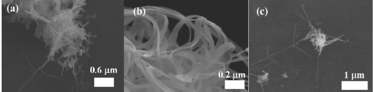
Figure 5.1. (A) Side-view and (B) top-view SEM images of Au nanothorns grown on Si. ... 67 Figure 5.2. SEM images of Au nanourchins grown on pre-roughened Si at different growth time. (A)-(B) 6 h, (C)-(D) 12 h, and (E)-(F) 18 h... 68 Figure 5.3. High Magnification SEM images of Au nanowires on nanourchins showing a pentagonal cross-section and a step structure on the side wall. ... 68 Figure 5.4 XRD of Au nanothorns grown on Si ... 69 Figure 5.5 (A) Emission current density as a function of applied electric field (J-E plots) on Au nanostructures; (B) corresponding Fowler-Nordheim (F-N) plots. ... 70
Chapter 1
Introduction
1.1 Introduction
Recently, copper has been an excellent material for IC interconnects in microelectronic industry due to its low electrical resistivity, high electro-migration resistance, and good thermal conductance relative to aluminum.1 Its good electrical and catalytic properties also employ as chemical catalyst and catalytic electrodes in organic syntheses and electro-catalytic reactions.2-5 Therefore, the exploration of copper is still an important subject in modern science and engineering.
One-dimensional (1-D) nanostructures are materials constrained in two dimensions to less than 100 nm. Within this category of nanomaterials, researchers discriminate between nanorods (NRs) with aspect ratios (length/diameter) less than 10, nanowires (NWs) with aspect ratios greater than 10, and nanotubes (NTs) with hollow interiors.6, 7 Research on nanostructures is primarily guided by three questions: (i) how can we produce large quantities of nanostructures with controllable sizes and shapes; (ii) what are the size- and shape-dependent physical and chemical properties of nanostructures; and (iii) how can the properties unique to nanostructures be exploited for applications? Pursuing answers to these questions has evolved into an active field of research now commonly referred to as nanoscience and nanotechnology.
1D nanomaterials have attracted intensive attention due to their unusual chemical and physical properties associated with the size and shape.8 Based on them, many researches have demonstrated that single one or arrays of 1D nanomaterials used as a building block in electronic, photonic, and sensing devices, which could attain miniaturization and enhance the
performance. Among them, metal nanomaterials displaying surface plasmon resonance (SPR),9 surface-enhanced Raman scattering (SERS),10 and electrochemical catalytic properties become a popular research subject. However, until now, there have been few reports regarding direct growth of 1D metal nanomaterials on hard electrodes and their potential application.
In this dissertation, novel metal nanostructures, such as Cu NBs, tetragonal nanopillars, Au nanothorns and nanourchins, that fabricated by surfactant assisted electrochemical methods, were revealed. Their shape dependent electrochemical catalysis and electron field emission (FE) performance will be explored.
1.2 Properties and Application of Metal Nanomaterials 1.2.1 Surface Area Effect
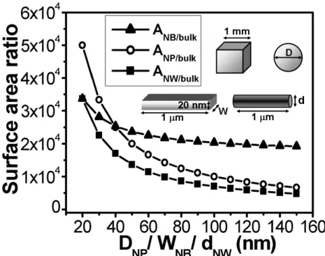
The high specific surface area is one of important characteristics of the nanostructures. The population of the atoms at the surfaces increases extremely as the dimension decreases. In order to compare to the influence of the morphology on surface areas, we estimated surface area ratios of NB, NW and nanoparticle (NP) to a bulk cube (1 mm3) as functions of corresponding geometric variables. Total amount of each nanostructure is equal to that of the bulk cube. As shown in Figure 1.1, the surface area of each nanostructure with comparable dimensions under 70 nm is at least 10,000 times larger than that of bulk cube. Interestingly, calculations show that NBs possess surface areas higher than NPs and NWs with comparable dimensions over 40 nm.
Although the surface area of NPs increases obviously as the diameter reduces from 40 nm, serious aggregation could happen and cause passivation of active sites in the process of crystal growth. On the other hand, the growth of 1D nanostructures and the formation of three-dimensional architectures on flat substrates increase the surface areas. This may boost the charge transfer happening between the interface of electrodes and species in solution.
Figure 1.1 Comparison of estimated surface area ratios of NB, NW and NP to a bulk cube (1 mm3) as functions of corresponding geometric variables: WNB (NB width, ▲), dNW (NW
diameter, ■), and DNP (NP diameter, ○). Total amount of each nanostructure is equal to that of
the bulk cube.
1.2.2 Adsorption and Catalytic Property
As mentioned above, nanomaterials display high surface-area-to-volume ratios. It means that most atoms expose to uncoordinated sites and stand under unstable states. It is required to passivate these active sites by adsorbing atoms or molecules at the surface. Hence, strong adsorption behavior and high active sites are important features of nanomaterials.
Heterogeneous catalysis is a common technique in the chemical industry. It can synthesize various chemicals and reduce production cost. Metal nanoclusters have been long used as heterogeneous catalyst in synthetic organic compounds. Solid supported palladium nanoclusters are a typical example.11 They can be employed in carbon-carbon coupling reaction, such as Suzuki Miyaura Cross-Coupling, Heck reaction and Stille coupling. Many
studies also showed Pd NPs displayed high catalytic efficiency for hydrogenation of alkene and oxidation of carbon monoxide. These properties were contributed to their excellent adsorption ability and high surface area.
Cu is a common catalyst because its abundance and chemical activity. In the syntheses of organic compounds, Cu NPs can catalyze the cyclization of Schiffs’ bases and condensation of iodo-benzene to biphenyl.2, 3 Besides, it can be used as a catalytic electrode for speeding up electro-reduction of oxygen and carbon dioxygen.4, 5 These interesting properties involving energy and environment issues have attracted intense attention on the possible usage of Cu.
1.2.3 Electrochemical Property and Sensing
Electrochemical reactions taking place at the interface between flat electrodes and electrolyte solutions are often impeded by diffusion process. Recent development of nanotechnology has promoted the fabrication of nanostructured electrodes with the high roughness (ratio of real surface area to geometric area). These electrodes display high electrochemical active surface areas and accelerate the electrochemical reaction.
NP-modified electrodes, such as copper, gold, silicon and platinum NP electrodes, used as excellent electron transfer mediators, were known examples.12-15 In recent years, 1D nanostructures have become interesting building blocks for constructing highly sensitive electrodes. Carbon nanotube (CNT), Pt NT, and Cu2O NW electrodes have been demonstrated
to be able to increase electro-oxidation ability of glucose and enhance the sensitivity for glucose detection.16-18 Besides, mesoporous and macroporous Pt electrodes also displayed the same electrocatalytic ability.19, 20 These designs of electrodes with high roughness increased undoubtedly high electro-catalytic active sites and boosted the kinetic-control reaction.
The morphologic effect of nanostructures on electrocatalytic activity is an important subject in material science. Each shape is correlated with which crystallographic facets exposed in the crystal. For example, three Pt electrodes, including (100), (110) and (111) single crystal,
displayed the different oxidation ability of hydrogen.21 Wang et al. synthesized the monodispersed Pt nanocubes, which are consistent of six {100} family planes. Compare to Pt NPs, they enhanced catalysis for oxygen reduciton.22 The morphology dependent electrochemical properties have started attracting more and more attention.
Cu NP electrodes could be used as catalytic electrodes for speeding up electro-reduction of oxygen and carbon dioxygen.4, 5 They could be employed as sensing electrodes for glucose, diphenol and amino acid.12, 23, 24
1.2.4 Surface Plasmon Resonance (SPR) Absorption
The study of the colors of metal NPs can be traced back to 19th century when Michael Faraday synthesize colloidal solutions of gold exhibiting colours ranging from ruby red to amethyst.25, 26 The various colors resulted from the surface plasmon band (SPB), which is a phenomenon observed in transmission, due to the presence of NPs, in solution or in the solid phase. For a special domain of frequency, NPs interact with incident light, resulting in a global scattering of it. This macroscopic feature can be explained by the collective resonance of the conduction electrons of the NP. A NP can be seen as an immobile and periodical cationic network in which a cloud of conducting electrons move. The latter are usually considered as free electrons.
Mie presented an analytical solution to Maxwell’s equations which describe a isolated spherical particle in 1908.27 Over the last three decades several numerical methods based on finite elements have been developed for overcoming the limitation in calculations of particles with arbitrary shape and multicomposition.28 Among those the discrete dipole approximation (DDA) has been proven to be an effective method for estimating the optical properties of metal particles in nanoscale.29 In most cases the extinction spectra of metal NPs under different conditions were simulated by the DDA method and compared with the experimental results.30 The investigation of the influence of particle shapes on surface SPR wavelengths
was also performed
The particle shape and size are an important factor to the SPR wavelength, and many papers concerning the size effect of the spherical nanoparticles have been published.31 Naturally, geometrical parameters also have strong influences on the SPR peaks, for example, triangle nanoplates. Schatz and co-workers have demonstrated that the increase of the side length of triangle nanoplates could lead their SPR peak to red shift by several hundred nanometers.32
This controllable optical property in terms of wavelength is quite exciting and interesting, and it enables the particles to be applied in biological sensing and drug delivery.33 Because the photons with near-IR wavelengths can harmlessly pass through biological tissues, nanoplates with high extinction coefficients at the target tissues will convert the near-IR photons to heat at high yields. So they can be used in photothermal cancer therapy and photothermally triggered drug release.
1.2.5 Surface-enhanced Raman Scattering (SERS)
The change in wavelength that is observed when a photon undergoes Raman scattering is attributed to the excitation (or relaxation) of vibrational modes of a molecule. Because different functional groups have different characteristic vibrational energies, every molecule has a unique Raman spectrum. In accordance with the Raman selection rule, the molecular polarizability changes as the molecular vibrations displace the constituent atoms from their equilibrium positions. The intensity of Raman scattering is proportional to the magnitude of the change in molecular polarizability. Thus, aromatic molecules exhibit more intense Raman scattering than aliphatic molecules.
Even so, Raman scattering cross sections are typically 14 orders of magnitude smaller than those of fluorescence; therefore, the Raman signal is still several orders of magnitude weaker than the fluorescence emission in most cases. Because of the inherently small intensity of the Raman signal, the sensitivity limits of available detectors, and the intensity of the excitation
sources, the applicability of Raman scattering was restricted for many years.
In 1977, Jeanmaire and Van Duyne demonstrated that the magnitude of the Raman scattering signal can be greatly enhanced when the scatterer is placed on or near a roughened noble-metal substrate.34 Strong electromagnetic fields are generated when the localized surface plasmon resonance (LSPR) of nanoscale roughness features on a silver, gold, or copper substrate is excited by visible light. When the Raman scatterer is subjected to these intensified electromagnetic fields, the magnitude of the induced dipole increases, and accordingly, the intensity of the inelastic scattering increases. This enhanced scattering process is known as surface-enhanced Raman (SER) scattering—a term that emphasizes the key role of the noble metal substrate in this phenomenon.
SER spectroscopy (SERS) can be exploited for sensitive and selective molecular identification. Recently, SERS has been used extensively as a signal transduction mechanism in biological and chemical sensing. Examples are trace analysis of pesticides, anthrax35, prostate-specific antigen36, glucose37, 38, and nuclear waste39. SERS has also been implemented for identification of bacteria40, genetic diagnostics41, and immunoassay labeling42-44. A miniaturized, inexpensive, and portable SERS instrument makes the technique practical for trace analysis in clinics, the field, and urban settings45.
1.2.6 Electron Field Emission (FE) Property
1D nanomaterials have a potential application as electron emitters in flat panel displays.46 The FE of electrons under applied electric fields is a quantum-mechanical phenomenon which can be understood as a tunneling process across the energy barrier between the vacuum and the emitter. In general, Fowler–Nordheim (F-N) equation is used to describe field emission characteristics of metals,47 which is expressed as J = A(β2
E2/Φ)exp(-BΦ3/2/βE), where J is the current density, E the applied field, Φ the work function of the metal, β the field enhancement factor, indicating the degree of field emission enhancement by the tip shape of the
electron-emitting edge, and A and B are constants. According to the equation, the F-N plot, ln(J/E2) versus 1/E, is expected to be a straight line.
In recent years, there are some researches demonstrating that metal NW arrays display FE properties with low threshold voltages and high enhancement factors.48, 49 It could be contributed to their high aspect ratio and good electrical conductance. Kim et al. further fabricated a FE display device of Cu NW arrays grown by chemical vapor deposition (CVD).50 These revealed that metal NWs are promising candidates as FE electron sources.
1.3 Synthetic Approaches to Novel Nanostructures of Metals
In order to study systematically unusual properties of nanostructures correlated with geometric shapes and dimensions, researchers have developed some methods to fabricate diverse and uniform nanostructures. Based on the reaction systems and employed technique, these methods were divided into three types: First one is Direct Hard Template Methods; Second one is Self-assembly Micelle and Capping Reagent Methods of Surfactants, and the last is Vapor-Solid Phase Reaction. We will introduce them with graphs summarized below.
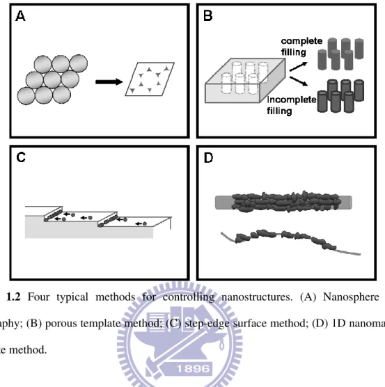
1.3.1 Direct Hard Template Methods
Figure 1.2 shows typical hard template-assisted methods, which is a simple way for fabricating 1D nanosructures.6 General templates involve in inorganic solid materials and organic molecules or polymer. The former includes anodic aluminum oxide (AAO), highly oriented pyrolytic graphite (HOPG) with step edge surface and inorganic 1D nanomaterials. The latter contains polystyrene (PS) nanosphere arrays, porous polycarbonate and DNA biomolecules. These templates used as frameworks are filled or coated with desired materials and then removed by physical or chemical etching. Array of patterned nanodot or high-aspect-ratio NWs are known examples. The advantages of these methods are easily
Figure 1.2 Four typical methods for controlling nanostructures. (A) Nanosphere array lithography; (B) porous template method; (C) step-edge surface method; (D) 1D nanomaterial template method.
controllable in product morphologies, low cost and reproducible. However, the drawback of complicated prefabrication and removal of templates existed. Four typical hard template methods shown in Figure 1.2 would be illustrated below.
1.3.1.1 Nanosphere array lithography
Nanosphere array lithography is an excellent method for fabricating regular tetragonal nanoparticle arrays. The PS nanoshpere colloids are dropped on a flat glass substrate. After evaporation of solvent, nanospheres self-assemble into a close-packing monolayer, as shown in Figure 1.2A. The arrays with the area of several millimeters could be used as a mask and coated with Ag by thermal evaporation. Ag nanoparticle arrays were formed after removal of nanosphere arrays.51 The uniformity of the size displays well-defined SPR peaks and
possessed potential application for biosensing.
1.3.1.2 Porous Materials
Porous template-assisted methods are an often used technique. Among porous templates, AAO has become the most general hard template because of controllable pore diameter and length and high porous density. Figure 1.2B shows the strategy for achieving 1D nanostructures by using AAO templates. NWs and NTs can be formed by full and part filled channels with desire materials, respectively.52, 53 For example, Gao et al. has employed AAO-assisted electrochemical deposition to fabricate Cu NW arrays.54, 55 Qie et al. successfully prepared Cu NTs by AAO-templated electroless deposition.56
1.3.1.3 Step-edge Surface Substrates
Figure 1.2C illustrates fabrication of NWs using highly oriented pyrolytic graphite (HOPG). Penner et al. found that metal ions favor nucleation and growth along the HOPG step edge. Therefore, they grew Cu and Ag NW arrays on HOPG surfaces by electrochemical deposition.57
1.3.1.4 1D Nanomaterials and Biomolecules
Figure 1.2D depicts that 1D nanomaterials are employed as templates to synthesize coaxial NWs. Day et al. have fabricated Ag coated carbon NTs by carbon NT-templated electrochemical deposition.58 Wolley et al. used DNA molecules with negative charges to attract Cu ions. Once reducing agent was added, Cu NPs would be formed and connected to form Cu NWs.59, 60
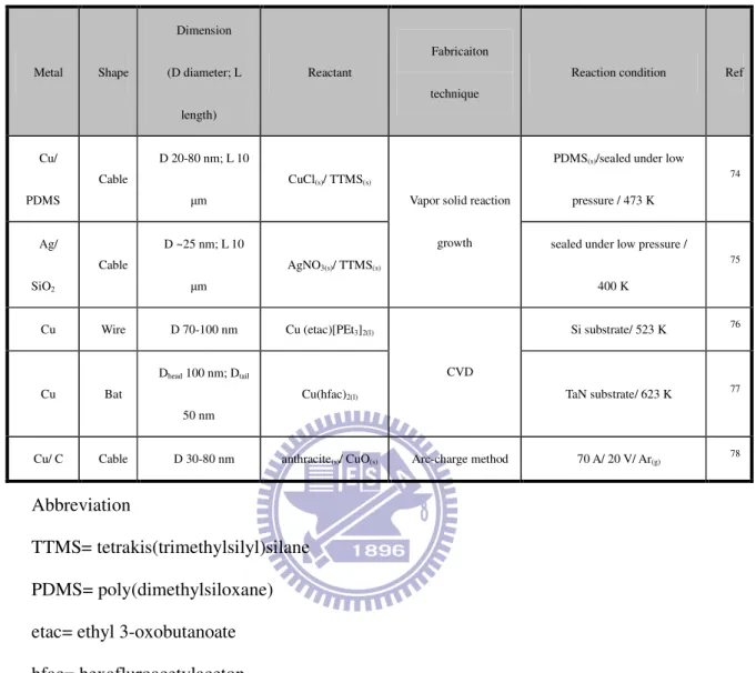
We summarize the direct hard template methods reported previously in Table 1.1.
Table 1.1 Direct template methods Metal Shape Dimension (D diameter; W width; T thickness; L length) reactant Fabrication technique Reaction condition (For example, template, system,
additives, temperature) Ref Ag Tetragonal particle T 52 nm; L 100 nm Ag(s) Nanosphere array lithography
PS nanosphere arrays, thermal coating 51
Cu Wire D 60 nm; L 30µm CuSO4(aq)
AAO, electrodeposition, electrolyte (H3BO3(aq)/ H2SO4(aq))
54,
55
Cu Tube D 300 nm CuSO4(aq)
AAO, electroless deposition, electrolyte (sodium tartrate(aq)/ NaOH(aq))
56 Ag Wire D 180-400 nm; L 30µm Commercial plating solution AAO, electrodeposition 52 Ag Helical wire D~10 nm AgNO3(aq) Porous template method AAO, electrodeposition、electrolyte (H3BO3(aq)) 53 Cu Wire D70-340 nm; L>10µm CuSO4(aq) Graphite, electrodeposition、electrolyte (Na2SO4(aq)) 57 Ag Wire D70-340 nm; L>10µm Ag2SO4(aq) Step-edge surface
template Graphite, electrodeposition、electrolyte (Na2SO4(aq) / saccharine(aq)) 57 Ag Wire D 60 nm; L 30µm AgNO3(aq) 1D nanomaterial template CNT, electrodeposition、electrolyte (KNO3(aq)) 58 Cu Wire D 3 nm Cu(NO3)2(aq)/ ascorbic acid(aq) DNA 59 Ag Wire D 30-50 nm AgNO3(aq)/ hydroquinone(aq) Bio-molecule template DNA 60
There are three indispensable components, metal salts, reducing agents and stabilizers in solution phase synthetic methods. Stabilizers, such as surfactants are important reagents not only for avoiding NP aggregation and directing anisotropic growth of nuclei. These methods have synthesized many nanomaterials, including nanocubes (NCs), NRs, NWs and triangular nanoplates (NPs). Based on difference of additives and fabrication procedures, they could be divided into five types, including self-assembly micelle, capping reagent, seed-mediated growth, polyol methods, galvanic reduction and hydrothermal methods.
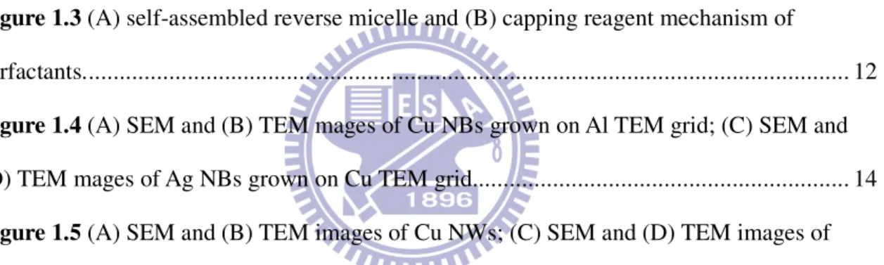
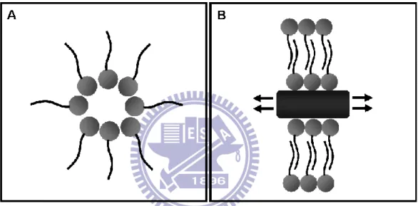
Figure 1.3 (A) self-assembled reverse micelle and (B) capping reagent mechanism of surfactants.
1.3.2.1 Micelle and Reverse Micelle Methods
This method, also called soft template method, is the early fabrication method of NPs. Surfactants have both hydrophilic and hydrophobic terminals and self-assemble into reverse micelles with various shapes in aqueous solution, as shown in Figure 1.3A. Nanocrystals are formed by reducing metal ions in this microreactor and stably dispersive in solution. Pileni et al. used rod-shape reverse micelles of AOT (sodium bis(2-ethylhexyl) sulfosuccinate) as soft templates in de-ionized water/ isooctane/ a trace of Cl- and synthesized Cu NRs.61
1.3.2.2 Seed-Mediated Growth
Murphy and coworkers have developed seed-mediated growth to fabricate and control 1D metal nanomaterials. When adding seeds into the mixture of metal salts, weak reducing agents and surfactants, the reaction would be activated and metal atoms could deposit selectively on the seeds to form anisotropic growth. NRs and NWs with an uniform diameter and aspect ratio were fabricated in the presence of 4 nm Ag seeds, AgNO3/ ascorbic acid growth solution
and cetyltrimethylammonium bromide (CTAB).9 Figure 1.3B depicts that bilayer structures of surfactants (CTAB) self-assemble adsorbed selectively on specific crystal facets and confine their growth. The relatively fast growth rate of uncapped sites caused formation of NRs or NWs. CTAB, called capping reagents, played an important role for controlling anisotropic crystal growth.
1.3.2.3 Polyol Methods
Polyols, which are high-boiling-point solvents and weak reducing agents, were used early for fabrication of metal and alloy colloid particles. When raising reaction temperature, polyol could increased the solubility of metal salt and reducing force. It is a convenient method to control the rate of nucleation and growth by adjusting reaction temperature. Xia and coworkers fabricated Ag NCs using ethylene glycol as a solvent and a reducing agent and adding AgNO3 and poly(vinyl pyrroli-done) (PVP) into thermal reflux reaction system.62, 63
Characterizations of infrared and X-ray photoelectron spectra confirmed that PVP, which adsorbed on Ag nanocrystal surfaces by O and N atoms, played the role of the capping reagent.64
1.3.2.4 Galvanic Displacement Reduction
A little different from typical homogeneous solution reaction system mentioned above, we evolved heterogeneous galvanic displacement reduction to fabricate Cu and Ag NBs, as
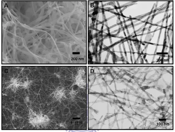
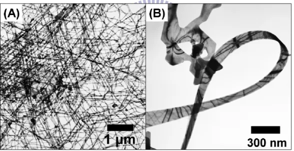
shown in Figure 1.4.65 Sacrificial metals oxidized itself and reduced the another metal ions at the interface of metal and solution. In general, fractal or dendrites would grow without any additives. We found that the products could be controlled to regular 1D nanostructures in the
Figure 1.4 (A) SEM and (B) TEM mages of Cu NBs grown on Al TEM grid; (C) SEM and (D) TEM mages of Ag NBs grown on Cu TEM grid.
presence of CTAC surfactant and inorganic acid. It is an excellent approach to grow and immobilize the diverse nanostructures on electrodes simultaneously. Multiple potential application such as sensing electrodes or SERS substrates could be expected.
1.3.2.5 Hydrothermal Methods
The autoclave is a common used reactor which can provide high pressure reaction condition under high temperature. Several literatures reported that it is possible to synthesize NWs in the presence of additives of small molecules or polymer surfactants as capping reagents. Liu,
15 Table 1.2 Self-assembly Micelle and Capping Reagent Methods of Surfactants
Metal Shape
Dimension (D diameter; W width; T thickness; L
length)
Reactant Fabrication technique
Reaction condition
Ref
Cu Rod D 5 nm; L 30 nm Cu(AOT)2/ N2H4 Micelle, reverse micelle \water/ isooctane/ trace Cl
- 61
Ag Rod, wire Drod 10-20 nm; Lwire 2-4µm AgNO3(aq)/ ascorbic acid(aq) Seed-assisted method Ag seed (4 nm)/ CTAB/ NaOH
9
Ag Cube ~D 80 nm AgNO3/ ethylene glycol PVP/ 433 K 63
Ag Wire D 30-40 nm; L 50µm AgNO3/ ethylene glycol
Polyol method
Pt seed/ PVP/ 433 K 6264
Cu Belt W 30-150 nm; T <15nm; L up to10-40µm CuCl2(aq)/ Al(s) CTAC/ HNO3 65
Ag Belt W30-100 nm; T <10nm; L up to 10µm AgNO3(aq)/ Cu(s)
Galvanic reduction
CTAC 65
Cu Wire D ~85 nm; L~µm CuSO4(aq)/ H3PO3(aq) glycerol/ SDBS/ NaOH / autoclave/ 393 K 66
Cu Wire D 90-120 nm; L 40-50 µm Cu(NO3)2(aq)/ N2H4(aq) ethylenediamine/ NaOH/ 333 K
67
Cu Wire D 30–100 nm; L ~mm CuCl2(aq) / octadecylamine(aq) Autoclave/ 393- 453 K
68
Cu Cable Dcore 80 nm; Dsheath 200 nm CuCl2(aq)/ PVA(aq) NaOH/ autoclave/ 473 K
71
Ag Wire D 100 nm; L up to 500 mm AgNO3(aq)/ glucose NaCl/ autoclave/ 453 K 69
Ag Wire D 30 nm AgNO3(aq)/ methenamine(aq)
Hydrothermal method
16
Ag Cable Dcore150-200 nm; L 100 µm AgNO3(aq)/ PVA(aq) autoclave / 433 K
72
Ag/C Cable D 200-250 nm; L 10 µm AgNO3(aq)/ α-D-glucose or β-cyclodextrine autoclave / 433 K
73
Abbreviation
AOT= sodium bis(2-ethylhexyl)sulfosuccinate CTAB= cetyltrimethylammonium bromide PVP= poly(vinyl pyrrolidone)
CTAC= cetyltrimethylammonium chloride SDBS= sodium dodecyl benzenesulfonate
gemini surfactant 16-3-16= 1,3- bis(cetyldimethylammonium) propane dibromide PVA= poly(vinyl alcohol)
Chang, Shi, Wang and Xu et al. fabricated a large amount of ultra-long Cu and Ag NWs by this method.66-70 Yu et al. used poly(vinyl alcohol) (PVA) as a reducing agent and a capping reagent and synthesized PVA coated Cu and Ag nanocables.71, 72 Instead of PVA, D-glucose or cyclodextrine would result in formation of Ag/C core-shell nanocables.73
Table 1.2 is a summary of self-assembly micelle and capping reagent methods of surfactants reported previously in literature.
1.3.3 Vapor-Solid Phase Reaction
Contrasting with solution reaction system, some researchers developed vapor-solid phase reactions to fabricate 1D nanomaterials. The typical techniques included vapor solid reaction growth (VSRG), chemical vapor deposition (CVD) and arc discharge method.
1.3.3.1 Vapor-Solid Reaction Growth (VSRG)
Our group developed a route of vapor solid reaction growth to synthesize Cu and Ag NWs in 2003.74, 75 CuCl encapsulated in poly(dimethylsiloxane) (PDMS) and tetrakis(trimethylsilyl) silane (TTMS, Si(SiMe3)4) as a reducing agent were sealed in a Pyrex tube under low pressure
and reacted in the furnace under 473 K for 6 h. After reaction, Cu/PDMS cables were produced, as shown in Figure 1.5A and B. In the reaction process, TTMS vapor diffused
Figure 1.5 (A) SEM and (B) TEM images of Cu NWs; (C) SEM and (D) TEM images of Ag/SiO2 nanocables.
across PDMS layers and reduced CuCl to form Cu atoms at the interface. These active Cu atoms aggregated and grew into NWs by PDMS directing. Subsequently, Ag/SiO2 nanocables
were also prepared by VSRG mechanism, as shown in Figure 1.5C and D.
1.3.3.2 Chemocal Vapor Deposition (CVD)
CVD is a traditional technique used to produce high-purity, high-performance solid materials, especially thin films in the semiconductor industry. Recently, it has become an important approach to grow 1D nanomaterials. Carbon NTs and silicon NWs grown by the vapor liquid solid (VLS) mechanism are well-known examples. In 2004, Choi et al. grew Cu NWs with the diameter of 70-100 nm on Si wafer using Cu(etac) [PEt3]2 (etac = ethyl
3-oxobutanoate) as a specific precursor.76 In 2006, Wang et al. used Cu(hfac)2 (hfac =
hexafluroacetylacetonate) as a precursor and grew Cu nanobats with pentagonal cross section on TaN.77 These free standing Cu NW arrays displayed electron FE properties. Besides, it is easy to construct FE panel device due to large area and selected area growth on Si. However, complicated syntheses of precursors and strict reaction condition restricted their development
Table 1.3 Vapor-solid phase method Metal Shape Dimension (D diameter; L length) Reactant Fabricaiton technique
Reaction condition Ref
Cu/ PDMS Cable D 20-80 nm; L 10 µm CuCl(s)/ TTMS(s)
PDMS(s)/sealed under low pressure / 473 K 74 Ag/ SiO2 Cable D ~25 nm; L 10 µm AgNO3(s)/ TTMS(s)
Vapor solid reaction
growth sealed under low pressure / 400 K
75
Cu Wire D 70-100 nm Cu (etac)[PEt3]2(l) Si substrate/ 523 K 76
Cu Bat Dhead 100 nm; Dtail 50 nm Cu(hfac)2(l) CVD TaN substrate/ 623 K 77
Cu/ C Cable D 30-80 nm anthracite(s)/ CuO(s) Arc-charge method 70 A/ 20 V/ Ar(g) 78
Abbreviation
TTMS= tetrakis(trimethylsilyl)silane PDMS= poly(dimethylsiloxane) etac= ethyl 3-oxobutanoate hfac= hexafluroacetylaceton
of application.
1.3.3.3 Arc Discharge Method
An electric arc is an electrical breakdown of a gas which produces an ongoing plasma discharge, resulting from a current flowing through normally nonconductive media such as air. Arc discharge process is the first and now widespread method of carbon NTs production. Wang et al. used the mixture of anthracite goal and CuO as the anode and evaporate them
under high temperature produced by DC arc discharge. Then Cu/C nanocables can be produced on the cathode.78
Table 1.3 is a summary of vapor-solid phase method reported in literature.
1.4 The Aim of This Thesis
In recent years, a large amount of researches with regard to Au and Ag nanomaterials has demonstrated interesting shape related physical and chemical properties. These materials have become candidates for new generation nanodevices. Their synthetic methods as mension above, nevertheless, require complex procedures, strict conditions, and unpleasantly operating equipments.
Cu and Au are highly applicable materials. Unfortunately, there are few reports regarding direct growth of 1D Cu and Au nanostructures on electrodes in the past years. We were devoted to developing a kind of method, which is able to create 1D Cu nanostructures and grow directly them on solid electrodes. It would promote more researches and development of functional devices of metal nanostructures.
In this thesis, we demonstrated that surfactant-assisted electrochemical methods, including galvanic displacement reduction and electrochemical deposition, provide a feasible approach to attain the desired goal: controllable growth of diverse Cu and Au nanostructures on solid electrodes. These products contains Cu NBs, pagoda-topped tetragonal nanopillar arrays, Au nanothorns, and nanourchins. Systematical observations by changing particularly additive concentration revealed that diffusion limited condition, surfactants, and nitric acid played a key role in controlling crystal morphologies.
Moreover, we are interested in how shape-dependent electrocatalysis and FE properties of these nanostructures are. These related studies would be presented in the following chapters.
1.5 References
1. Liu, R.; Pai, C.-S.; Martinez, E. Solid-State Electron. 1999, 43, 1003.
2. Kidwai, M.; Bansal, V.; Saxena, A.; Aerry, S.; Mozumdar, S. Tetrahedron Lett. 2006, 47, 8049.
3. Dhas, N. A.; Raj, C. P.; Gedanken A. Chem. Mater. 1998, 10, 1446.
4. Gattrell, M.; Gupta, N.; Co, A. Journal of Electroanal.l Chem. 2006, 594, 1. 5. Jiang, I.; Brisard, G. M. Electrochim.a Acta 2007, 52, 4487.
6. Xia, Y.; Yang, P.; Sun, Y.; Wu, Y.; Mayers, B.; Gates, B.; Yin, Y.; Kim, F.; Yan, H. Adv.
Mater. 2003, 15, 353.
7. Chen, J.; Wiley, B. J.; Xia, Y. J. Am. Chem. Soc. 2007, 23, 4120.
8. Xia, Y.; Yang, P.; Sun, Y.; Wu, Y.; Mayers, B.; Gates, B.; Yin, Y. K., F.; Yan, H. Adv.
Mater. 2003, 15, 353.
9. Murphy, C. J.; Jana, N. R. Adv. Mater. 2002, 14, 80.
10. Tao, A.; Kim, F.; Hess, C.; Goldberger, J.; He, R. G.; Sun, Y. G. X., Y. N.; Yang, P. D.
Nano Lett. 2003, 2, 1229.
11. Yin, L. X.; Liebscher, J. Chem. Rev. 2007, 107, 133.
12. Zhao, J.; Wang, F.; Yu, J. J.; Hu, S. S. Talanta 2006, 70, 449. 13. Jena, B. K.; Raj, C. R. Chem. Eur. J. 2006, 12, 2702.
14. Wang, G.; Mantey, K.; Nayfeh, M. H.; Yau, S. T. Appl. Phy. Lett. 2006, 89, 24. 15. Hrapovic, S.; Liu, Y. L.; Male, K. B.; Luong, J. H. T. Anal. Chem. 2004, 76, 1083. 16. Ye, J. S.; Wen, Y.; Zhang, W. D.; Gan, L. M.; Xu, G. Q.; Sheu, F. S. Electrochem.
Commun. 2004, 6, 66.
17. Yuan, J. H.; Wang, K.; Xia, X. H. Adv. Funct. Mate. 2005, 15, (5), 803-809.
18. Zhuang, Z. J.; Su, X. D.; Yuan, H. Y.; Sun, Q.; Xiao, D.; Choi, M. M. F. Analyst 2008,
133, 126.
20. Song, Y. Y.; Zhang, D.; Gao, W.; Xia, X. H. Chem. Eur. J. 2005, 11, 2177.
21. Bard, A. J.; Faulkner, L. R., Electrochemical methods: Fundamentals and Applications 2nd ed.; John Wiley & Sons Inc., New York, 2001.
22. Wang, C.; Daimon, H.; Lee, Y.; Kim, J.; Sun, S. J. Am. Chem. Soc. 2007, 129, 6974. 23. Zen, J. M.; Chung, H. H.; Kumar, A. S. Analy. Chem. 2002, 74, 1202.
24. Zen, J. M.; Hsu, C. T.; Kumar, A. S.; Lyuu, H. J.; Lin, K. Y. Analyst 2004, 129, 841. 25. Moores, A.; Goettmann, F. New J. Chem. 2006, 30, 1121.
26. Faraday, M., Philos. Trans. 1857, 147, 145. 27. Mie, G., Ann. Phys. 1908, 25, 377.
28. Waterman, P. C. Phys. Rev. D 1971, 13, 825-39.
29. Yang, W.-H.; Schatz, G. C.; Van Duyne, R. P. J. Chem. Phys. 1995, 103, 869.
30. Duval Malinsky, M.; Kelly, K. L.; Schatz, G. C.; Van Duyne, R. P. Analy. Chem. 2001,
105, 2343.
31. Messinger, B. J.; von Raben, K. U.; Chang, R. K.; Barber, P. W. Phy. Rev. B 1981, 24, 649.
32. Jin, R.; Charles Cao, Y.; Hao, E.; Metraux, G. S.; Schatz, G. C.; Mirkin, C. A. Nature 2003, 425, 487.
33. West, J. L.; Halas, N. J. Analy. Chem. 2003, 5, 285.
34. Jeanmaire, D. L.; Vanduyne, R. P. J. Electroanaly. Chem.1977, 84, 1.
35. Zhang, X. Y.; Young, M. A.; Lyandres, O.; Van Duyne, R. P. J. Am. Chem. Soc. 2005,
127, 4484.
36.Grubisha, D. S.; Lipert, R. J.; Park, H. Y.; Driskell, J.; Porter, M. D. Analy Chem 2003, 75, 5936.
37. Shafer-Peltier, K. E.; Haynes, C. L.; Glucksberg, M. R.; Van Duyne, R. P., J. Am. Chem.
38. Yonzon, C. R.; Haynes, C. L.; Zhang, X. Y.; Walsh, J. T.; Van Duyne, R. P. Analy. Chem. 2004, 76, 78.
39. Bao, L. L.; Mahurin, S. M.; Haire, R. G.; Dai, S. Ana. Chem. 2003, 75, 6614. 40. Jarvis, R. M.; Brooker, A.; Goodacre, R. Analy. Chem. 2004, 76, 5198.
41. Culha, M.; Stokes, D.; Allain, L. R.; Vo-Dinh, T. Analy. Chem. 2003, 75, 6196. 42. Cao, Y. W. C.; Jin, R. C.; Mirkin, C. A. Science 2002, 297, 1536.
43. Doering, W. E.; Nie, S. M. Anal. Chem. 2003, 75, 6171.
44. Mulvaney, S. P.; Musick, M. D.; Keating, C. D.; Natan, M. J. Langmuir 2003, 19, 4784. 45. Young, M. A.; Stuart, D. A.; Lyandres, O.; Glucksberg, M. R.; Van Duyne, R. P., Can. J.
Chem. 2004, 82, 1435.
46. Choi, W. B.; Chung, D. S.; Kang, J. H.; Kim, H. Y.; Jin, Y. W.; Han, I. T.; Lee, Y. H.; Jung, J. E.; Lee, N. S.; Park, G. S. J. Chem. Phys. 1999, 75, 3129.
47. Fowler, R. H.; Nordheim, L. W. Proc. R. Soc. A 1928, 119, 173.
48. Dangwal, A.; Pandey, C. S.; Muller, G.; Karim, S.; Cornelius, T. W.; Trautmann, C. Appl.
Phys. Lett. 2008, 92, 063115-3.
49. Wang, J.-H.; Yang, T.-H.; Wu, W.-W.; Chen, L.-J.; Chen, C.-H.; Chu, C.-J.
Nanotechnology 2006, 17, 719.
50. Kim, C.; Gu, W. H.; Briceno, M.; Robertson, I. M.; Choi, H.; Kim, K. Adv. Mater. 2008,
20, 1859.
51.Haes, A. J.; Zhao, J.; Zou, S.; Own, C. S.; Marks, L. D.; Schatz, G. C.; VanDuyne, R. P., J.
Phys. B 2005, 109, 11158.
52. Choi, J.; Sauer, G.; Nielsch, K.; Wehrspohn, R. B.; Gosele, U. Chem. Mater. 2003, 15, 776.
53. Wu, Y.; Livneh, T.; Zhang, Y. X.; Cheng, G.; Wang, J.; Tang, J.; Moskovits, M.; Stucky, G. D. 2004, 4, 2337.
55. Gao, T.; Meng, G. W.; Wang, Y. W.; Sun, S. H.; Zhang, L.. J. Phys.Cond. Matter 2002,
14, 355.
56. Li, N.; Li, X. T.; Yin, X. J.; Wang, W.; Qiu, S. L. Solid State Commun. 2004, 132, 841-844.
57.Walter, E. C.; Murray, B. J.; Favier, F.; Kaltenpoth, G.; Grunze, M.; Penner, R. M. J. Phys.
Chem. B 2002, 106, 11407.
58. Day, T. M.; Unwin, P. R.; Wilson, N. R.; Macpherson, J. V. J. Am. Chem. Soc. 2005, 127, 10639.
59. Monson, C. F.; Woolley, A. T. Nano Lett. 2003, 3, 359.
60. Braun, E.; Eichen, Y.; Sivan, U.; Ben-Yoseph, G. Nature 1998, 391, 775.
61.Pileni, M. P.; Ninham, B. W.; Gulik-Krzywicki, T.; Tanori, J.; Lisiecki, I.; Filankembo, A.
Adv. Mater. 1999, 11, 1358.
62. Wiley, B.; Sun, Y. G.; Mayers, B.; Xia, Y. Chem. Eur. J. 2005, 11, 454. 63. Sun, Y.; Xia, Y. 2002, 298, 2176.
64. Sun, Y. G.; Mayers, B.; Herricks, T.; Xia, Y. N. 2003, 3, 955.
65.Huang, T. K.; Cheng, T. H.; Yen, M. Y.; Hsiao, W. H.; Wang, L. S.; Chen, F. R.; Kai, J. J.; Lee, C. Y.; Chiu, H. T. Langmuir 2007, 23, 5722.
66. Liu, Z.; Yang, Y.; Liang, J.; Hu, Z.; Li, S.; Peng, S.; Qian, Y. J. Phys. Chem. B 2003, 107, 12658.
67. Chang, Y.; Lye, M. L.; Zeng, H. C. Langmuir 2005, 21, 3746.
68. Shi, Y.; Li, H.; Chen, L.; Huang, X. Sci. and Technol. Adv. Mater. 2005, 6, 761. 69. Wang, Z.; Liu, J.; Chen, X.; Wan, J.; Qian, Y. Chem. Eur. J. 2005, 11, 160. 70. Xu, J.; Hu, J.; Peng, C.; Liu, H.; Hu, Y. J. Colloid Interface Sci. 2006, 298, 689. 71. Gong, J.; Luo, L.; Yu, S. H.; Qian, H.; Fei, L. J. Mater. Chem. 2006, 16, 101. 72. Luo, L. B.; Yu, S. H.; Qian, H. S.; Zhou, T. J. Am. Chem. Soc. 2005, 127, 2822.
73. Yu, S. H.; Cui, X. J.; Li, L. L.; Li, K.; Yu, B.; Antonietti, M.; Coelfen, H. Adv. Mater. 2004, 16, 1636.
74. Yen, M. Y.; Chiu, C. W.; Hsia, C. H.; Chen, F. R.; Kai, J. J.; Lee, C. Y.; Chiu, H. T. Phys.
Lett. 1999, 75, 627.
75. Hsia, C. H.; Yen, M. Y.; Lin, C. C.; Chiu, H. T.; Lee, C. Y. J. Am. Chem. Soc. 2003, 125, 9940.
76. Choi, H.; Park, S. H. J. Am. Chem. Soc. 2004, 126, 6248.
77. Wang, J. H.; Yang, T. H.; Wu, W. W.; Chen, L. J.; Chen, C. H.; Chu, C. J.
Nanotechnology 2006, 17, 719.
Chapter 2
Growth of Cu Nanobelts by Surfactant-Assisted Galvanic Reductions
2.1 Introduction
Nanobelts are interesting one dimensional materials under intensive investigation.1-15 There are many reports regarding the syntheses and applications of nanobelts of semiconductors and main group elements.1-7 On the other hand, transition metal nanobelts are much less reported. The only known example is the preparation of Ni nanobelt by a hydrothermal method and Au nanobelt by a sonochemical method.8,9 Here, we report a surfactant assisted synthesis of single crystalline cubic phase 3C Cu nanobelt via galvanic reductions of CuCl2(aq) solutions in the presence of CTAC (cetyltrimethylammonium
chloride) by Al(s). To our knowledge, this is the first example of Cu nanobelt reported to this
date. We expect the metallic nanobelts, with metallic conductivity and increased surface area, may find future applications as electrodes in sensing devices,16,17 as contacts for molecular electronic circuits,18 in surface-enhanced Raman scattering (SERS) spectroscopy,19,20 and in metal-polymer composites for electromagnetic interference (EMI) shielding layers.21
2.2 Experimental
2.2.1 Preparation of Cu Nanobelts
A summary of growth conditions is listed in Table 2.1. Growth of Cu NBs by galvanic reduction of CuCl2(aq) by Al(s) in the presence of CTAC and HNO3 (Belt-6) is described
below as a typical example.
Table 2.1 Summary of growth conditions of Cu nanostructures.
Sample CuCl2 (mM) CTAC (mM) HNO3 (mM) Temperature (oC) Time (h)
Wire-1 5 0.45 - 17 3 Wire-2 5 1.78 - 17 3 Wire-3 5 3.56 - 17 3 Wire-4 5 1.78 - 17 3.5 Belt-1 5 1.78 0.5 17 20 Belt-2 5 1.78 5 17 20 Belt-3 5 1.78 30 17 20
CTAC (Taiwan Surfactant, 1.78 x 10⁻³ M) and HNO3 (SHOWA, 5 x 10⁻³ M) in a glass vial.
Immediately, the mixture turned light blue. The mixture was then placed in a water bath controlled at 290 K. An Al TEM grid (Agar, 200 mesh), cleaned in H3PO4(aq) (Riedel-de
Haen, 5 % w.t., 3 mL) for 2 m and rinsed by deionized water, was immersed into this mixture. The reaction was controlled at 290 K without stirring. The Al surface turned dark red gradually. After 24 h, the Al grid was removed and rinsed by deionized water.
2.2.2 Characterization
The air-dried samples were investigated by SEM (Hitachi S-4000 at 25 kV and JEOL JSM-6330F at 15 kV), EDS (Oxford Link Pentafet) and TEM (JEOL JEM-2010F at 200 kV and JEOL JEM-4000EX) instruments. The colloid was analyzed by an X-ray diffractometer (XRD, Bruker AXS D8 Advance) and a particle analyzer (Honeywell Microtrac UPA 150).
2.3 Results
Figure 2.1 Low and high magnification SEM images of Cu nanostructures growing in solution of different CTAC concentration. (a)-(b) 0.45 mM (Wire-1), (c)-(d) 0.178 mM (Wire-2), and (e)-(f) 3.56 mM (Wire-3).
CuCl2 in an aqueous solution was reduced by an Al transmission electron microscopic
(TEM) grid (Agar, 200 mesh) at 290 K. As the reaction progressed, the Al surface turned dark red gradually.
Figure 2.1 shows SEM images of Sample Wire-1, Wire-2, Wire-3 in an aqueous solution of CTAC concentration at 0.45 mM, 1.8 mM, and 3.6 mM, respectively. Figure 2.1a and b show that Wire-1 has a particle layer formed on the Al grid in 0.45 mM CTAC(aq) solution.
Figure 2.2 (a) SEM image of the products growing at 3.5 h (Wire-4); (b) EDS of the area marked by A in (a); (c) EDS of the area marked by B in (a).
Figure 2.1c and d show that Wire-2 grows a little of NWs with a length of about 2 µm from a particle layers as CTAC concentration increases to 1.8 mM. Instead, Wire-3 prepared in higher CTAC concentration, 0.36 mM grew less NWs, as shown in Figure 2.1e and f. It indicates that appropriate CTAC concentration assisted formation of NWs.
When elongating growth time, there are many amorphous clusters depositing on Wire-4, as shown in Figure 2.2 (a). EDS analysis suggests that NWs indicated by A consist of Cu and amorphous clusters marked by B are composed of aluminum oxide. Obviously, deposition of aluminum oxide disturbs the growth of Cu NWs.
In order to avoid interference of aluminum oxide, we choose to add nitric acid to increase dissolution of aluminum oxide in solution. Sample Belt-1, Belt-2, and Belt-3 were prepared
Figure 2.3 SEM images of Cu nanostructures growing in the presence of different HNO3
concentration. (a) 0.5 mM (Belt-1); (b) 5.0 mM (Belt-2); and (c) 30.0 mM (Blet-3).
in 0.5, 5, and 30 mM HNO3 aqueous solution, respectively. Figure 2.3 shows amorphous
aluminum oxide disappears and 1D nanostructures appear on Al grid. Especially, Figure 2.3(b) shows a ribbon-like nanostructure grows densly across the grid. Generally, the nanobelt has a width of 30 - 150 nm, a thickness less than 15 nm and a length up to 10 µm. Thus, the width-to-thickness and the length-to-width ratios are as high as 10 and 300, respectively. Normally, these characters are maintained across an entire nanobelt.
2.3.2 XRD analysis
XRD pattern of Belt-3 are shown in Figure 2.4. It shows combination of two-set patterns. One has peaks at 2θ = 38.4o, 44.8o, 65.1o, and 78.2o, which are assigned to Al (111), (200), (220) and (311) reflections, respectively (JCPDF 04-0787). Al reflection is from TEM Al grid. The other has peaks at 2θ = 43.4o, 50.6o, 74.2o, which are assigned to Cu (111), (200), and (220) reflections, respectively.22 Calculated lattice constant a, 0.361 nm, is close to the reported value of Cu.22 This XRD study suggested that 3C Cu was grown on the Al.
2.3.3 TEM characterization
Low magnification TEM image in Figure 2.5A display an interlacing net composed of Cu NBs. Figure 2.5B shows characteristic ripple-like images from the strains of belt bending.
Figure 2.4. XRD pattern of Cu NBs grown on an Al grid ( * = unknown)
Figure 2.5. (A) Low and (B) high magnification TEM images of Cu NBs.
This feature was frequently observed in TEM studies for thin samples.1-15
In Figure 2.6, a set of excellent quality TEM images of a selected NB, examined from a properly adjusted angle, are shown. In Figure 2.6A, ripple-like contrasts arise from belting are observed again.1-15 The SAED in Figure 2.6B displays a spot pattern from the rectangular region marked by a dotted arrow in Figure 2.6A. This can be indexed to be
Figure 2.6. (A) TEM image of Cu nanobelts, (B) [1,1,0] zone SAED, and (C) HRTEM image
of the marked rectangular region pointed by the dotted arrow in (A).
[1,1,0] zone axis of Cu, with an estimated lattice parameter of 0.36 nm. From the pattern, the apparent growth direction of the NB is determined to be along [1,-1,3] direction. From two tiny dim spots indicated by the arrows in Figure 2.6B, a d-spacing of 0.25 nm is estimated. This indicates the presence of a minute quantity of Cu2O, which has a {1,1,1}
spacing distance close to the observed value.23 The origin is proposed to be some oxidation on the nanobelt surface. Figure 2.6C presents an HRTEM image from the marked region in Figure 2.6A. The directions of planes {1,-1,1} and {-1,1,1} are identified from the fringes. The dihedral angle of 70.5o is equal to the theoretical value of an f.c.c. structure. The {1,1,1} d spacing is measured to be 0.21 nm, close to the literature value of Cu, 0.208 nm.22
Scheme 2.1. Proposed growth mechanism of Cu nanobelt.
2.3.4 Proposed Growth Mechanism
We discovered that adding HNO3 to the reaction mixture is important for the process.
Without it, a large amount of aluminum oxide deposit blocked the Al surface and interrupted the Cu growth. The acidic environment probably assists the aluminum oxide dissolution so that active Al metal surface can be exposed. The addition of CATC is also essential to the NB formation. Without the surfactant, only dendridic structures were produced. The physical forms of Al metal did not affect the Cu NB growth much. We tried several types of Al, including powders, foils and plates. They all showed similar results.
The preparation of both Cu NB is dependent on the presence of CTAC. Without it, the uncontrolled growths produce dendridic structures.24-27 A generalized CTAC assisted NB growth is presented in Scheme 1 to describe the overall growth process. Galvanic reduction
of Cu2+(aq) by more active Al(s) to form Cu NBs is described. The Cu2+(aq) ions are reduced,
then nucleate into Cu metal on the Al surface. The reaction is spontaneous due to a positive redox potential Eo = 2.00 V, for the reaction 3 Cu2+(aq) + 2 Al(s) → 3 Cu(s) + 2 Al3+(aq).28
CTAC molecules probably adsorb selectively on two crystallographically opposite facets of a Cu seed to form a bilayer interface structure.29, 30 Through the ionic ends of the surfactant molecules, one side of the CTAC bilayer binds to the Cu surface while the other side interfaces with the aqueous medium. Between two ionic sides, the aliphatic chains form an inner nonpolar sheet. This specific arrangement restricts the deposition of Cu atoms on the CTAC passivated facets. Consequently, the Cu crystal grows within the CTAC bilayer constructed soft template and develops into a NB.
2.4 Conclusion
In summary, we have demonstrated the first time that Cu NB can be grown via simple galvanic reductions of the corresponding metal ions by active metals in the presence of CTAC in aqueous solutions. Both CTAC and HNO3 molecules are essential ingredients to
2.5 References
1. Wang, Z. L., Adv. Mater. 2003, 15, 432.
2. Pan, Z. W.; Dai, Z. R.; Wang, Z. L. Science 2001, 291, 1947.
3. Shi, W. S.; Peng, H. Y.; Wang, N.; Xu, C. P.; Li, L.; Lee, C. S.; Lee, S. T. J. Am.
Chem. Soc. 2001, 123, 11095.
4. Ma, Y.; Qi, L.; Shen, W.; Ma, J. Langmuir 2005, 21, 6161.
5. Cao, X. B.; Xia, Y.; Zhang, S. Y.; Li, F. Q. Adv. Mater. 2004, 16, 649.
6. Mo, M.; Zeng, J.; Lin, X.; Yu, W.; Zhang, S.; Qian, Y. Adv. Mater. 2002, 14, 1658. 7. Zhang, M.; Wang, Z.; Xi, G.; Ma,D.; Zhang, R.; Qian, Y. J. Cryst. Growth 2004,
268, 215.
8. Liu, Z.; Li, S.; Yang, Y.; Peng, S.; Hu, Z.; Qian, Y Adv. Mater. 2003, 15, 1946. 9. Zhang, J. L.; Du, J. M.; Han, B. X.; Liu, Z. M.; Jiang, T.; Zhang, Z. F. Angew.
Chem. Int. Ed. 2006, 45, 1116.
10. Wang, Y.; Zhang, L.; Meng, G.; Liang, C.; Wang, G.; Sun, S. Chem. Commmun. 2001, 24 ,2632.
11. Xie, Z.; Wang, Z.; Ke, Y.; Zha, Z.; Jiang, C. Chem. Lett. 2003, 32, 686. 12. Sun, Y.; Mayers, B.; Xia, Y. Nano Lett. 2003, 3, 675.
13. Law, M.; Sirbuly, D.; Johnson, J.; Goldberger, J.; Saykally, R.; Yang, P. Science 2004, 305, 1269.
14. Yan, H.; Justin, J.; Law, M.; Saykally, R.; Yang, P. Adv. Mater. 2003, 15, 1907. 15. Law, M.; Kind, H.; Kim, F.; Messer, B.; Yang, P. Angew. Chem. Int. Ed. 2002, 41,
2405.
16. Zen, J. M.; Chung, H. H.; Kumar, A. S. Anal. Chem. 2002, 74, 1202. 17. Zen, J. M.; Chung, H. H.; Kumar, A. S. Analayst 2000, 125, 1633.
18. Tour, J. M Molecular Electronics: Commercial Insights, Chemistry, Devices,
19. Kneipp, K.; Wang, Y.; Kneipp, H.; Perelman, L. T.; Itzkan, I.; Dasari, R.; Feld, M. S. Phys. Rev. Lett. 1997, 78, 1667.
20. Nie, S. M.; Emory, S. R. Science 1997, 275, 1102.
21. Bagwell, R. M.; McManaman, J. M.; Wetherhold, R. C. Compos. Sci. Tech. 2006,
66, 522.
22. Joint Committee for Powder Diffraction (JCPDS) File No. 04-0836, International Center for Diffraction Data (ICDD), 1982.
23. JCPDS File No. 05-0667, ICDD, 1953.
24. Ben-Jacob, E.; Garik, P. Nature 1990, 343, 523.
25. Shin, H. C.; Dong, J.; Liu, M. Adv. Mater. 2003, 15, 1610. 26. Wang, S.; Xin, H. J. Phys. Chem. B 2000, 104, 5681.
27. Ma, Y.; Che, C. M.; Chao, H. Y.; Zhou, X.; Chan, W. H.; Shen, J. Adv. Mater. 1999, 11, 850.
28. Bard, A. J.; Faulkner, L. R. Electrochemical Methods: Fundamentals and
Applications, John Wiley & Sons, New York, 1980.
29. Gao, J.; Bender, C. M.; Murphy, C. J. Langmuir 2003, 19, 9065. 30. Nikoobakht, B.; El-Sayed, M. A. Langmuir 2001, 17, 6368.