318 IEEE ELECTRON DEVICE LETTERS, VOL. 24, NO. 5, MAY 2003
A High Efficient 820 nm MOS Ge
Quantum Dot Photodetector
B.-C. Hsu, Student Member, IEEE, S. T. Chang, Student Member, IEEE, T.-C. Chen, P.-S. Kuo, P. S. Chen, Z. Pei, and
C. W. Liu, Senior Member, IEEE
Abstract—A Ge quantum dot photodetector has been demon-strated using a metal–oxide–semiconductor (MOS) tunneling structure. The oxide film was grown by liquid phase deposition (LPD) at 50 C. The photodetector with five-period Ge quantum dot has responsivity of 130, 0.16, and 0.08 mA/W at wavelengths of 820 nm, 1300 nm, and 1550 nm, respectively. The device with 20-period Ge quantum dot shows responsivity of 600 mA/W at the wavelength of 850 nm. The room temperature dark current density is as low as 0.06 mA/cm2. The high performance of the photodetectors at 820 nm makes it feasible to integrate electroop-tical devices into Si chips for short-range opelectroop-tical communication.
Index Terms—Liquid phase deposition, MOS diode, quantum dot photodetector.
I. INTRODUCTION
I
NTEREST in silicon-based optoelectronic devices has grown rapidly in the last decade [1]. Si photodetectors at 820–850 nm wavelengths have been reported by several groups [2], [3]. However, they have limited detection efficiency and wavelength range due to the large absorption length 16 m of Si at 820 nm [2] and the forbidden absorption at 1300 and 1550 nm. The incorporation of Ge into Si can increase the cutoff wavelength and enhance the absorption efficiency [4]. In this paper, metal–oxide–semiconductor (MOS) tunneling structures [5] with Ge quantum dots have been investigated as the photodetector. Low temperature liquid phase deposited (LPD) SiO is used as the gate oxide film to avoid high tem-perature thermal oxidation, which induces Ge-related defects during oxidation.II. DEVICEFABRICATION
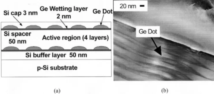
The Si/Ge quantum dots were prepared by ultrahigh-vacuum chemical vapor deposition (UHVCVD) on p-type Si (001) sub-strates. The structure is shown in Fig. 1(a) and the TEM image of the Ge quantum dot is shown in Fig. 1(b). After a Si buffer layer of 50 nm, five periods of Ge/Si bilayers were grown to form the self-assembled Ge dots at 600 C under the Stranski–Krastanov (SK) growth mode [6]. To separate the Ge layers, a Si spacer
Manuscript received February 3, 2003; revised February 28, 2003. This work was supported in part by the National Science Council of Taiwan, R.O.C., under Contracts 91-2120-E-002-007 and 91-2215-E-002-027. The review of this letter was arranged by Editor T.-J. King
B.-C. Hsu, S. T. Chang, T.-C. Chen, P.-S. Kuo, and C. W. Liu are with the Department of Electrical Engineering and Graduate Institute of Electronics En-gineering, National Taiwan University, Taipei, Taiwan, R.O.C.
P. S. Chen, Z. Pei, and C. W. Liu are with the ERSO/ITRI, Hsinchu, Taiwan, R.O.C. (e-mail: [email protected]).
Digital Object Identifier 10.1109/LED.2003.812558
Fig. 1. (a) Structure of five-layer Ge quantum dot devices prepared by UHVCVD. (b) TEM micrograph of Ge quantum dot samples.
Fig. 2. Process flow of liquid phase deposition.
layer with the thickness of 50 nm was used. A 3 nm (nominal thickness) Si cap was deposited as a top layer on self-assembled Ge dots for the subsequent growth of oxide by LPD. All layers grown by UHVCVD were p-type doped with an estimated con-centration on the order of 1 10 cm .
The MOS diodes had Al gate electrodes with various circular areas defined by photolithography. To avoid strain relaxation and Ge segregation, low-temperature oxide process is required. LPD [7], [8] is a promising low-temperature process for SiO formation with low thermal budget, low cost, and high throughput. Fig. 2 shows the experimental flow diagram of the LPD process in this work. Details can be found in the literature [8].
III. DEVICEOPERATION
Fig. 3 shows the room temperature current–voltage ( – ) characteristics of the five-period Ge quantum dot NMOS de-tector under 820 nm lightwave exposures with different light in-0741-3106/03$17.00 © 2003 IEEE
HSU et al.: MOS Ge QUANTUM DOT PHOTODETECTOR 319
Fig. 3. I–V characteristics of the Ge quantum dot MOS detector under 820 nm lightwave exposures with different light intensity. The inset shows that the photo-generated carriers can be collected by the gate electrode through lateral drift and diffusion.
Fig. 4. Band diagram of a Ge quantum dot NMOS detector under inversion bias. The transient response of a typical Si MOS detector under 850 nm pulse measurement is shown in the inset.
tensity. The LPD oxide thickness of the device was 1.5 nm. Be-cause the Al electrode would block and reflect the light shined directly on the device, the fiber is pointed to the edge of the gate electrode and the photogenerated carriers can be collected by the electrode due to lateral drift and diffusion of the carriers, as shown in the inset of Fig. 3. The room temperature dark cur-rent density is as low as 0.06 mA/cm for the five-period Ge quantum dot MOS devices, while the dark current of typical Ge pin devices is 20 mA/cm [9]. Note that the photocurrent is relatively independent of applied voltage, and the device can operate close to zero volt bias. Fig. 4 shows the band diagram of a Ge quantum dot NMOS detector under inversion bias. The photoelectrons are generated in the deep depletion region, and are swept toward the gate electrode. The photoelectrons tunnel from the active layer to the Al gate electrode due to trap-assisted tunneling in the LPD oxide.
It is noted that the device area is 3.2 10 cm and the il-luminated area is 64 m (fiber diameter is 9 m). Since the fiber is pointed to the edge of the gate electrode and the de-pletion width is smaller than 1 m at 2 V positive gate bias, most excited carriers are collected by the electrode through dif-fusion and the device speed is limited. The FWHM is 2 ns for
Fig. 5. (a) Device responsivity versus different light intensity operated in 820, 1300, and 1550 nm, respectively. (b) The dark and photo current at 850 nm of the MOS detector with 20-period Ge quantum dots.
the typical Si MOS detector under 850 nm pulse measurement, as shown in the inset of Fig. 4. A finger electrode structure and silicon-on-insulator (SOI) substrate could be used instead of cir-cular electrode and Si substrate to increase the device speed. The excited carriers between two fingers can be collected quickly by the electrode because the large electric field within the de-pletion region, and the excited carriers deep in the substrate are eliminated by using a SOI substrate. It is also noted that since the band offset in Si/Ge heterojunctions is mainly in the valence band, the electrons in the conduction band are less scattered by the conduction band discontinuity, as compared to holes in the valence band. The complex structure of the valence band due to the Ge wetting layer and quantum dots has an insignificant ef-fect on our NMOS detector, in which electron transport is dom-inant. The dark current of the NMOS Ge quantum dot detector is determined by thermal generation rate through the defects in the deep depletion region and the interface states [10].
Fig. 5(a) is the room temperature responsivity of a device with five-period Ge quantum dots under 820, 1300, and 1550 nm lightwave exposure, respectively. The MOS Ge quantum dot de-tector shows an external quantum efficiency of 20% at 820 nm. For 1300 nm and 1550 nm detection wavelengths, the respon-sivity of MOS Ge quantum dot detectors drops to 0.16 and 0.08 mA/W, respectively, due to the insufficient thickness of active layers. The Si MOS detector was also fabricated to de-termine the responsivity enhancement of Ge quantum dot struc-tures. With the insertion of Ge quantum dots into Si devices, the device efficiency at 820 nm increases by a factor 10 as compared to the Si device without Ge incorporation, and the Si detector has no response at 1300 and 1550 nm. To enhance the device responsivity, MOS detectors with 20-period Ge quantum dot were fabricated using the same process. The dark and photo current at 850 nm are shown in Fig. 5(b). The responsivity at 850 nm reaches 600 mA/W, but the responsivity at 1300 and 1550 nm are similar to that of a 5-period Ge quantum dot device.
IV. CONCLUSIONS
The five-period Ge quantum dot MOS device can detect the wavelengths of 820 nm, 1300 nm, and 1550 nm with responsivity of 130, 0.16, and 0.08 mA/W, respectively. The responsivity at 850 nm reaches 600 mA/W using a 20-period Ge quantum dot absorption layer. The gate oxide is grown by low-temperature LPD and the Ge quantum dot structures are prepared by UHVCVD. At inversion gate bias, the dark current
320 IEEE ELECTRON DEVICE LETTERS, VOL. 24, NO. 5, MAY 2003
of the detector is limited by the generation rate of minority carriers in the depletion region. The room temperature dark current density is as low as 0.06 mA/cm .
ACKNOWLEDGMENT
The authors would like to acknowledge C. L. Lin and Prof. L. A. Wang of Optical Fiber Communication and Sensor Lab (OFC&S), Department of Electrical Engineering, National Taiwan University, for the responsivity measurement of the detectors.
REFERENCES
[1] R. A. Soref, “Silicon-based optoelectronics,” Proc. IEEE, vol. 81, pp. 1687–1706, Dec. 1993.
[2] M. Yang et al., “High speed silicon lateral trench detector on SOI sub-strate,” in IEDM Tech. Dig., 2001, pp. 547–550.
[3] C. L. Schow, R. Li, J. D. Schaub, and J. C. Campbell, “Design and imple-mentation of high-speed planar Si photodiodes fabricated on SOI sub-strates,” IEEE J. Quantum Electron., vol. 35, pp. 1478–1482, Oct. 1999. [4] B.-C. Hsu, S. T. Chang, C.-R. Shie, C.-C. Lai, P. S. Chen, and C. W. Liu, “High efficient 820 nm MOS Ge quantum dot photodetectors for short reach integrated optical receivers,” in IEDM Tech. Dig., 2002, pp. 91–94.
[5] C. W. Liu, W. T. Liu, M. H. Lee, W. S. Kuo, and B. C. Hsu, “A novel photodetector using MOS tunneling structures,” IEEE Electron Device Lett., vol. 21, pp. 307–309, June 2000.
[6] T. I. Kamins, D. A. A. Ohlberg, R. S. Williams, W. Zhang, and S. Y. Chou, “Positioning of self-assembled, single-crystal, germanium islands by silicon nanoimprinting,” Appl. Phys. Lett., vol. 74, pp. 1773–1775, 1999.
[7] H. Nagayama, H. Honda, and H. Kawahara, “A new process for silica coating,” J. Electrochem. Soc., vol. 135, p. 2013, 1988.
[8] J.-S. Chou and S.-C. Lee, “Improved process for liquid phase deposition of silicon dioxide,” Appl. Phys. Lett., vol. 64, pp. 1971–1973, 1994. [9] S. Fama, L. Colace, G. Masini, G. Assanto, and H.-C. Luan, “High
per-formance germanium-on-silicon detectors for optical communications,” Appl. Phys. Lett., vol. 81, no. 4, pp. 586–588, 2002.
[10] C.-H. Lin, B.-C. Hsu, M. H. Lee, and C. W. Liu, “A comprehensive study of gate inversion current of metal-oxide-silicon tunneling diodes,” IEEE Trans. Electron Devices, vol. 48, pp. 2125–2130, Sept. 2001.