A Design of 2.6 GHz Auto-Biasing Cascode Class-E PA with V
dd/AM and V
dd/PM
Compensations in EER System
Wen-An Tsou, Wen-Shen Wuen, and Kuei-Ann Wen
Department of Electronics Engineering National Chiao Tung University
Hsinchu, Taiwan, R.O.C. e-mail: watsou.ee93g@nctu.edu.tw Abstract—An auto-biasing cascode class-E PA which can
compensate the Vdd/AM and Vdd/PM distortion resulting from
supply modulation has been proposed. The output voltage of auto-biasing control circuit is generated and varied linearly with PA’s supply voltage so that the cascode transistor is degenerated into a resistance and the PA’s nonlinear distortion can be compensated. The simulation result shows that the distortion is compensated evidently and the system co-simulation demonstrated that system EVM can be improved from -17 to -19dB. Also, the drain efficiency of the PA can be improved 15% within small supply voltage range.
Keywords- Trnsmitters, class-E power amplifier, envelope elimination and restoration (EER).
I. INTRODUCTION
To increasing the data rate, recent wireless communication systems allow the carried information encoded in both amplitude and phase of the RF signal and therefore a linear PA is required. The linearity achieved in such amplifiers by operating below their maximum output power has the drawback of lower efficiency and hence reduced battery lifetime. EER (or Polar) transmitter architecture can be used to overcome the trade-off between linearity and efficiency and to cope with the deficiency of CMOS technology. For reliability issues of PAs, device stacking is a popular way to reduce voltage stress on each device so as to lower device degradations [1][2]. However, a conventional (fixed-biasing) cascode class-E PA used in EER or Polar system will introduce the Vdd/AM and Vdd/PM
distortion. Here, the measured amplitude and phase distortion is due to Vdd (supply voltage) modulation and
hence referred to as Vdd/AM and Vdd/PM respectively.
Furthermore, the distortion will severely degrade the system emission performance.
The popular technique of compensating the nonlinear distortion is the digitally predistortion technique [3] or using feedback topology [4] in EER/Polar systems, however, other design challenges will be derived. Therefore, an auto-biasing cascode class-E PA which can compensate the Vdd/AM and
Vdd/PM distortion without complicating the system has been
proposed. The auto-biasing control circuit can degenerate the cascode transistor of the PA into a resistance and, therefore, the Vdd/AM and Vdd/PM distortion can be compensated. A
system co-simulation platform of EER with OFDM-based
signal in ADS-Ptolemy is shown in Fig. 1. In practice, the architecture would need to be more complex than shown in Fig. 1. Nevertheless, the purpose of this simulation platform is to investigate the effects of the PA’s nonlinear distortion so that system imperfections like the amplitude error of the envelope detector and the bandwidth requirement of envelope path have been optimized. The circuit principle and nonlinear distortion of conventional cascode class-E PA is described in Section II. Section III elaborates the detailed description and distortion compensations of the proposed PA. Finally, section IV draws conclusions.
II. CONVENTIONAL CASCODE CLASS-EPOWER AMPLIFIER
The class-E power amplifier achieves 100% drain efficiency theoretically and is a good candidate for EER or polar transmitters. A conventional structure of cascode class-E PA was designed at 2.6GHz carrier frequency by using UMC 0.18µm RFCMOS model as shown in Fig. 2 where the transistor M1 operates as a switch and the output load
network shapes the output waveform to prevent simultaneous high voltage and current, which minimizes the power dissipation. The transistor M2 biased with a voltage Vdc is
stacked to release the voltage stress of devices at the high voltage swings. The mathematical equations used in the design are presented in [5][6].
A. Supply Voltage Modulation of Cascode Class-E PA As supply modulation, the transistor M2 has two input
signals, VGS2 and VDS2, so that the inherent transconductance
and capacitance are involved simultaneously with VGS2 and
VDS2 and thus can be modeled with nonlinear components
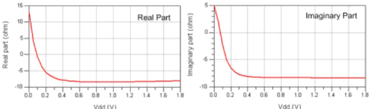
such as CDB, CGB, CSB, CGS and CGD as shown in Fig. 3. The
nonlinear components cause the nonconstant impedance Z (=VDS2/IDS2, where VDS2 and IDS2 indicate drain to source
voltage and current of the transistor M2, respectively.) and
the real part and imaginary part of impedance Z are shown in Fig. 4. Within small Vdd range, the transistor M2 operates in
deep triode region and occupies extremely small voltage VDS2 so that the impedance is closed to constant. As Vdd
increasing gradually, the transistor M2 moves to saturation
region so that the large VDS2 and IDS2 result in the nonconstant
impedance. Moreover, the nonconstant impedance induces the nonlinear distortion at the drain node of the transistor M2
and the amplifier’s output signal accompanies with this
2009 Pacific-Asia Conference on Circuits,Communications and System
978-0-7695-3614-9/09 $25.00 © 2009 IEEE DOI 10.1109/PACCS.2009.109
distortion. In EER or polar systems, the PA’s nonlinear distortion has crucial impacts on envelope restoration [7]. The linearity of the amplifier was investigated by sweeping the supply voltage from 0 to 1.8V. The output voltage vs. Vdd
(Vdd/AM) relationship is shown in Fig. 5. The output signal
level changes according to Vdd, therefore the envelope can be
restored. However, Fig. 5 reveals that the output voltage related to Vdd is nonlinear. Also, the voltage deviation can be
seen at Vdd=0, which may result in additional distortion at
low envelope levels.
When the amplifier’s supply voltage deviates from its optimum value (1.8V), maximum Vdd/PM changes by 21
degrees/V and 18 degrees of the phase shift down to 0.5V. Within the range of 0-0.5V, the Vdd/PM characteristic is
highly nonlinear and the phase shift can be as large as 67 degree. These characteristics demonstrate that low envelope levels are harder to reconstruct than high envelope level.
Figure 1. EER architecture.
Figure 2. Conventional cascode class-E PA.
Figure 3. Equivalent model of the transistor M2.
Figure 4. Real part and imaginary part of the impedance Z (VDS2/IDS2).
Figure 5. Vdd/AM and Vdd/PM of conventional cascode class-E PA.
B. Nonlinear distortin effect in EER Transmitter
Simulations were performed in ADS-Ptolemy using an IEEE 802.11a OFDM-based waveform (36Mbits/s, 52 carriers, 16-QAM modulation scheme and modulation bandwidth=20MHz) up-converted to 2.6GHz frequency band. The histogram of envelope signal as shown in Fig. 6 has 93 % from 0.5-1.8V and the mean voltage is 1V. The time delay of 2.8ns is estimated according to the argument in [8] as intermodulation distortion (IMD) of -40dBc. The EER architecture shown in Fig. 1 with the conventional cascode class-E PA was simulated. The EVM result is -17dB (-19dB for the specification) and the received constellation is shown in Fig. 7. The result reveals that the amplifier’s distortions cause the received symbol to move closer to additional constellation point than the one transmitted. This demonstrates that the Vdd/AM and Vdd/PM imperfections are
sufficient to cause the violation of system specification.
Figure 6. Histogram of the envelope voltage.
Figure 7. The received constellation before compensation.
III. PROPOSED CASCODE CLASS-EPOWER AMPLIFIER A circuit technique, different from canceling the PA’s nonlinear distortion with system architectures, to compensate the Vdd/AM and Vdd/PM distortion by automatically biasing
the cascode class-E PA has been presented. The auto-biasing control circuit is to adjust the impedance Z to prevent the distortion production due to variations of the tansconduct-ance and capacittansconduct-ance.
A. Auto-Biasing Control Circuit and Cascode Class-E PA Fig. 8 shows the schematic of cascode class-E PA combined with auto-biasing control circuit. The function of auto-biasing control circuit is to generate the voltage Vco, so
that this voltage can equal the envelope voltage Vdd plus a
half of the voltage Vc. Therefore, as Vdd variations, the gate
voltage biased by the voltage Vco can operate the transistor
M2 as a resistance. Thus, the constant impedance Z can be
obtained. The simulation result in Fig. 9 shows that the real part and imaginary part of impedance Z are close to the constant except in the small Vdd range. It indicates that the
transistor M2 with the variant transconductance and
capacitance are degenerated into a resistance. Therefore, the nonlinear distortion at the drain node is compensated so as to at the PA’s output node. The compensated Vdd/AM and
Vdd/PM distortion is shown in Fig. 10. The output voltage is
linearly related to Vdd and the phase shift within the range of
0.5-1.8V is improved from 18 degrees to 3 degrees even the voltage deviation at Vdd=0 and large phase shift in the range
of 0-0.5V. Hence, the proposed auto-biasing control circuit combined with a cascode class-E PA can evidently compensate the amplifier’s Vdd/AM and Vdd/PM distortion as
supply modulation.
Figure 8. (a) Auto-biasing cascode class-E PA, (b) the schematic of auto-biasing control circuit.
Figure 9. Real part and imaginary part of the impedance Z (VDS2/IDS2)
after compensation.
Figure 10. Vdd/AM and Vdd/PM of auto-biasing cascode class-E PA.
B. Compensated Vdd/AM and Vdd/PM in EER Transmitter
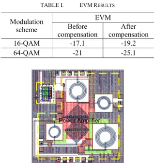
Subsequently, the same EER transmitter was simulated, but with the auto-biasing cascode class-E PA to reconstruct the envelope. The received constellation shown in Fig. 11 is closer to the transmitted constellation point and the EVM is -19dB. Comparing with the result of Fig. 7, it can clearly see that the nonlinear distortion impacts strongly the EVM with a noisy constellation. Results of EVM are reported in Table I. Therefore, it demonstrated that the auto-biasing cascode class-E power amplifier can effectively compensate the Vdd/AM and Vdd/PM distortion as supply modulation in EER
transmitter.
C. Circuit Implement and Performance
Fig. 12 shows the layout of the proposed 2.6GHz auto-biasing cascode class-E PA. Total die area including pads is 2.16 mm². This work is implemented by using UMC 0.18µm Mixed-Signal/RF CMOS 1P6M technology.
The output power of auto-biasing PA with the variable supply voltage is shown in Fig. 13 and the output amplitude is proportional to supply voltage (Pout α Vdd²). The maximum
output power is 16dBm and it also reveals that the output power of auto-biasing PA is without reduction as compared with conventional PA. The proposed PA draws 62mA current consumption with supply voltage 1.8V as shown and its current increases linearly with Vdd as shown in Fig. 14.
However, conventional PA consumes the larger dc current in small Vdd range and this causes the reduction of PA’s drain
efficiency. PA’s drain efficiency can be expressed as DC DC dd out DC out I 1 I V P % 100 P P Efficiency= × ∝ ∝ (1) when output power Pout and supply voltage Vdd are the same
as supply modulation, drain efficiency is inversely proportional to IDC. The simulated result of drain efficiency
shown in Fig. 15 has demonstrated the statement of (1). In small Vdd range, due to auto-biasing PA consuming the
smaller dc current, the efficiency of auto-biasing PA is larger than conventional PA and has the maximum improvement of 15%. Hence, the proposed auto-biasing cascode class-E power amplifier not only compensates the Vdd/AM and
Vdd/PM distortion but also improves drain efficiency.
IV. CONCLUSIONS
An auto-biasing cascode class-E PA by adjusting the equivalent impedance of the cascode transistor to compensate the Vdd/AM and Vdd/PM distortion in EER
transmitter has been proposed. System co-simulation result also demonstrates that the auto-biasing PA can effectively improve the system EVM performance.
Figure 11. The received constellation after compensation.
TABLE I. EVMRESULTS
Modulation scheme
EVM Before
compensation compensationAfter 16-QAM -17.1 -19.2 64-QAM -21 -25.1
Figure 12. Layout of the auto-biasing cascode class-E PA.
Figure 13. The output power of PA.
Figure 14. The dc current consumption of PAs.
Figure 15. Drain efficiency of PAs. REFERENCES
[1] T. Sowlati and D. M. W. Leenaerts, “A 2.4 GHz in 0.18-µm CMOS self-biased cascode power amplifier with 23-dBm output power,” IEEE Int. Solid-State Circuits Conf. Digest of Tech. Papers, Feb. 2002, pp. 294-295.
[2] A. Mazzanti, L. Larcher, R. Brama and F. Svelto, “Analysis of reliability and power efficiency in cascode class-E PAs,” IEEE J. Solid-State Circuits, vol. 41, no. 5, pp. 1222-1229, May 2006. [3] S. Hietakangas, T. Rautio and T. Rahkonen, “1 GHz class E RF
power amplifier for a polar transmitter,” IEEE 24th Norchip Conference, Nov. 2006, pp. 5-9.
[4] T. Sowlati, D. Rozenblit, R. Pullela, M. Damgaard, E. McCarthy, D. Koh, D. Ripley, F. Balteanu and I. Gheorghe, “Quad-Band GSM/GPRS/EDGE polar loop transmitter,” IEEE J. Solid-State Circuits, vol. 39, no. 12, pp. 2179-2189, Dec. 2004.
[5] D. K. Su and W. J. McFarland, “An IC for linearizing RF power amplifiers using envelope elimination and restoration,” IEEE J. Solid-State Circuits, vol. 33, Issue 12, pp. 2252-2258, Dec. 1998.
[6] N. O. Sokal, “Class-E switching-mode high-efficiency tuned RF/microwave power aplifier,” IEEE Int. Microwave Symp. Digest, vol. 2, 11-16 June 2000, pp. 779-782.
[7] A. Diet, C. Berland, M. Villegas and G. Baudoin, “EER architecture specifications for OFDM transmitter using a class E amplifier,” IEEE Microwave and Wireless Components Letters, vol. 14, no. 8, pp. 389-391, Aug. 2004.
[8] F. H. Raab and D. J. Rupp, “Class-S high-efficiency amplitude modulator,” RF Design, vol. 17, no. 5, pp. 70-74, May 1994.