loops (PLLs). The jitter-measurement structure is based on a novel time-to-digital converter (TDC) which has a high resolution. A small area overhead is also achieved using the voltage-controlled oscillator and the loop filter of the PLL under test as parts of the TDC. The experiment result shows that the resolution is about 1 ps and that the measurement error is smaller than 20%.
Index Terms—Analog built-in self-test (BIST), jitter
measure-ment, on-chip measuremeasure-ment, phase-locked loop (PLL) BIST, time-to-digital converter (TDC).
I. INTRODUCTION
P
HASE-LOCKED loops (PLLs) are extensively employed as clocking signal sources in digital and mixed-signal circuits. The clock jitter of PLLs is one of the most impor-tant properties to be measured. As clock speeds have reached gigahertz in recent years, measuring the clock jitter using an external high-speed test equipment is becoming increasingly expensive.The built-in self-test (BIST) approach becomes an alternative means of measuring the clock jitter at low cost [1]–[14]. The most common method of measuring a jitter is based on the time-to-digital converter (TDC). Several TDCs are available for BIST, including those that are based on the adjustable delay line [1], [14], the Vernier delay line (VDL) [2], [6], the component-invariant VDL [3], [4], the analog-to-digital converter (ADC) [9], the cyclic pulsewidth modulator [11], and the time-to-voltage converter (TVC) [13].
The method that is based on the adjustable delay line is the simplest approach implementing the TDC [1], [14]. A digitally controlled variable delay line is adopted to obtain the cumula-tive distribution function of the jitter. In this design, the resolu-tion is limited by the delay of one delay buffer. The VDL was developed to increase the resolution [2], [6]. The component-invariant VDL TDC was also developed to solve the problems of mismatch and large area overhead [3], [4]. However, both the VDL and the component-invariant VDL require an additional digital-to-analog converter (DAC) to generate varying analog control voltages to fine-tune the delay time of the delay line; thus, the additional DAC, calibration, and control mechanism are needed.
Manuscript received January 5, 2007; revised May 29, 2007.
The authors are with the Department of Electrical and Control Engineering, National Chiao Tung University, Hsinchu 300, Taiwan, R.O.C.
Color versions of one or more of the figures in this paper are available online at http://ieeexplore.ieee.org.
Digital Object Identifier 10.1109/TIM.2007.910109
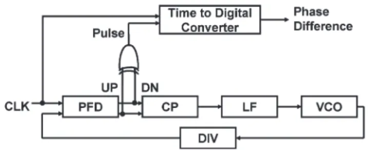
Fig. 1. BIST circuit for measuring jitter of CP-PLL.
The ADC converts the clock jitter into digital codes by applying a sine wave to the ADC input and using the test signal as the ADC clock [9]. This approach exhibits high resolution and short test time but cannot directly measure a high-speed signal because it utilizes an off-chip ADC rather than an on-chip high-speed ADC. The TVC approach transforms a phase difference into a voltage using a charge pump (CP) and a capacitor (C) [13]. The voltage is further converted into a digital code using a specially designed ADC. The approach uses its analog characteristics to achieve high resolution. However, the circuit is more complex, and the parameters must be carefully selected.
Fig. 1 shows the TVC approach for measuring the clock jitter. This circuit detects the jitter by transforming the phase differences into pulses that are as wide as the magnitude of the phase differences. Unfortunately, when the jitter becomes sufficiently small to be in the dead zone of the XOR gate, or when the phase offset is larger than the jitter, it does not function. To solve the problem, a novel TDC structure to detect the jitter on the order of picoseconds or in the presence of a large phase offset is proposed.
Section II describes the TDC structure. Section III presents in detail the circuit structure. Section IV presents the experimental results. Section V draws conclusions.
II. TIME-TO-DIGITALCONVERTER
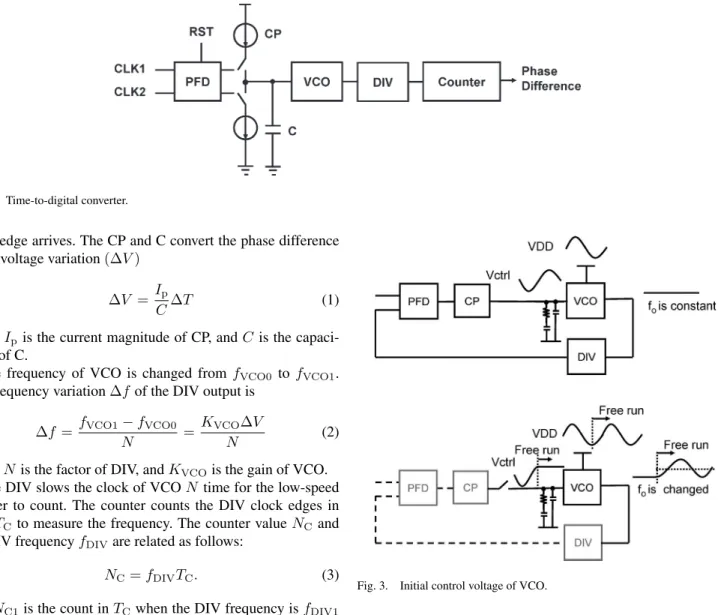
The use of TDC to measure the jitter is the concept that underlies the BIST circuits. The TDC detects each phase dif-ference between the redif-ference clock and the clock under test to obtain the histogram of the jitter. As shown in Fig. 2, the TDC is composed of a phase-frequency detector (PFD), a CP, a C, a voltage-controlled oscillator (VCO), a divider (DIV), and a counter.
Two clocks CLK1 and CLK2 with some phase difference ∆T are input to the PFD. The phase difference is detected using the PFD only once, and the PFD is disabled before the next 0018-9456/$25.00 © 2008 IEEE
clock edge arrives. The CP and C convert the phase difference into a voltage variation (∆V )
∆V = Ip
C∆T (1)
where Ipis the current magnitude of CP, and C is the capaci-tance of C.
The frequency of VCO is changed from fVCO0 to fVCO1. The frequency variation ∆f of the DIV output is
∆f = fVCO1− fVCO0
N =
KVCO∆V
N (2)
where N is the factor of DIV, and KVCOis the gain of VCO. The DIV slows the clock of VCO N time for the low-speed counter to count. The counter counts the DIV clock edges in time TCto measure the frequency. The counter value NCand the DIV frequency fDIVare related as follows:
NC= fDIVTC. (3) If NC1is the count in TCwhen the DIV frequency is fDIV1 and if NC0is the count when the DIV frequency is fDIV0, then the frequency variation and the count difference ∆N are related as follows:
∆N = NC1− NC0= (fDIV1− fDIV0)TC= ∆f TC. (4) Equations (1), (2), and (4) yield the relationship between the count difference ∆N and the phase difference ∆T
∆T = N C
KVCOIPTC
∆N. (5)
The count difference yields the phase difference. One count difference means that a phase difference of kRES has been detected. The coefficient kRES represents the measurement resolution kRES= ∆T ∆N = N C KVCOIPTC
(picoseconds per count). (6) Because of process variation, the gain of VCO, the current magnitude of CP, and the capacitance of C of the fabricated chip will not be the same as the values in the simulation result. To calibrate the TDC and to obtain the accurate coefficient kRES of the fabricated chip, a pulse with the known pulsewidth ∆T
Fig. 3. Initial control voltage of VCO.
is input to the CP. The count difference ∆N is obtained, and the accurate coefficient is calculated.
The proposed TDC measures the small phase differences between the two clocks because the dead zone of the PFD is zero. The zero-dead-zone PFD is implemented using two edge-triggered resettable D flip-flops. The Up (UP) and Down (DN) signals of the PFD are simultaneously high for a short time, as shown in Fig. 7. Even if the phase difference of the two inputs is nearly zero, the UP and DN signals still have short pulses to turn on the transistors of CP. The difference between their pulsewidths represents the phase difference. Thus, a zero dead zone is achieved.
However, if there is a current mismatch between the charg-ing and dischargcharg-ing paths of CP, the PLL will automatically compensate the mismatch by keeping the pulsewidths of these two short pulses different; therefore, the constant phase offset between CLKA and CLKB occurs. The phase offset can also be measured and separated from the jitter by observing the histogram of the phase differences. The mean in the histogram represents the phase-offset error, and the variance represents the jitter.
The parameters of CP and C should be carefully designed to have a proper detection range. If the current is too large and
Fig. 4. Proposed BIST circuit.
the capacitance is too small, the voltage variation will be out of the control voltage range of VCO. If the current is too small and the capacitance is too large, then the voltage variation will be too small, and the noise on the node of C will induce more measurement error.
TCis the parameter that determines the measurement resolu-tion. For longer TC, the measurement resolution is higher, but the effect of the leakage current increases, and the test time also increases.
The C and the VCO have a large area and dominate the area overhead of the BIST circuit. Fortunately, the loop filter, the VCO, and the DIV of the PLL under test can be adopted as parts of the TDC. Therefore, the area overhead is reduced. The PFD and the counter only comprise several logic gates; therefore, the total area is small.
There is a noise source that deteriorates the accuracy of this approach. The TDC utilizes the VCO and the loop filter of the PLL under test as parts of the circuit, but the initial value of the VCO control voltage is not constant due to the power-supply noise and the PLL-tracking ability. Fig. 3 shows the timing diagram of the VCO in the PLL and the noise of the power supply. Assume that the frequency of the noise is much lower than the loop bandwidth of the PLL. A phenomenon is observed that the voltage of the loop filter is varying in the opposite phase of the power-supply noise for canceling the effect of the noise and keeping the frequency of the VCO constant. It is reasonable because the frequency of the supply noise is much lower than the loop bandwidth; thus, the PLL can keep the frequency of the VCO constant and can lock the phase of the reference clock. If the loop of the PLL is opened at a particular time, the voltage of the loop filter is kept in a particular value by the Cs of the loop filter at that moment. This value becomes the initial value of the VCO control voltage of the TDC. However, this value is determined by the power-supply-noise voltage at the moment when the loop is opened; therefore, the value is not predictable. The frequency deviation of the VCO caused by the noise is derived as the power-supply noise multiplied by the VCO power-supply gain KVCO2. The VCO power-supply gain is defined as the VCO frequency variation over the power-supply
variation. For example, the peak value of the power-supply noise is 1 mV, and the VCO power-supply gain is 200 MHz/V. The maximum frequency deviation of the VCO is 0.2 MHz, and the maximum frequency deviation of the DIV output is 12.5 kHz if the DIV factor is 16. After a counting time of 200 µs, the count of the counter deviates from its ideal value for 12.5k· 200 µ = 2.5. Then, 2.5 is multiplied by the mea-surement resolution of 1 ps/count to be 2.5 ps. Therefore, the measurement error is 2.5 ps. The measurement error ∆T1 is derived as follows:
∆T1= VnKVCO2TCkRES=
VnKVCO2N C
KVCOIP
(7) where Vnis the power-supply noise.
The only parameter which can be adjusted to suppress the measurement error is the current of CP; thus, the current should be designed as large as possible. If a complete avoidance of this noise source is desired, an additional C, instead of the loop filter of the PLL under test, should be used in generating a constant initial control voltage of the VCO.
III. CIRCUITDESCRIPTION
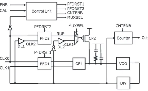
As shown in Fig. 4, the BIST circuit comprises three main parts—TDC, control unit, and calibration circuit. The TDC is composed of delay buffer1 (DL1), PFD2, MUX, CP2, loop filter, VCO, and DIV. The loop filter, VCO, and DIV are also parts of the PLL under test. The control unit is the finite-state machine using CLK0 as its clocking signal. The calibration circuit calibrates the coefficient of the measurement resolution, which is determined by the parameters of the CP current of the CP2, the equivalent capacitance of the loop filter, and the VCO gain. The calibration circuit is composed of the VCO, DIV, delay buffer2 (DL2), MUX, CP2, and loop filter.
A. Time-to-Digital Converter
As shown in Fig. 4, TDC is composed of DL1, PFD2, MUX, CP2, loop filter, VCO, and DIV. The VCO, loop filter, and
Fig. 6. PFD2 circuit design.
Fig. 7. Timing behavior of PFD2.
Fig. 8. Timing behavior of circuit with DL1.
DIV of the PLL under test are reused as components of the TDC circuit to minimize the area overhead. When the phase difference between CLK0 and CLK1 is detected, the PLL is immediately shut down by disabling PFD1. After that, both loop filter and VCO function as parts of the TDC. Fig. 5 shows the modified PFD, which can be disabled using a reset signal.
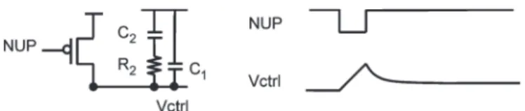
The TDC structure is modified to simplify the calibration process and to enlarge the current capacity. CP2 is designed as a single switch that is controlled using the signal NUP only. Figs. 6–8 show the modified circuit and timing behavior. DL1 delays CLK1 to generate signal CLK2. The CLK2 is always lagging behind CLK0; thus, UP or NUP contains all of the timing information about CLK0 and CLK1, and signal DN can be neglected.
As shown in Fig. 9, the C of TDC is replaced by loop filter. The loop filter can be modeled as a C with capacitance C
C = C1+ C2. (8)
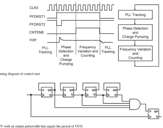
tracking step is the lock-in or pull-in process of the PLL. In step 1, PFD1 is turned on, and PFD2 is turned off to allow the PLL to track the phase of the reference clock. In phase-detection step, the PFD1 is turned off, and the PFD2 is turned on to enable the TDC to detect the phase difference between the reference clock and the feedback clock. CP2 pumps some charge to the loop filter, and the voltage of the loop filter settles down to a particular value. Then, the control unit proceeds to step 3. In this step, the counter is turned on to count the number of pulses from the DIV output.
The finite-state machine uses the negative edge of the refer-ence clock as its clocking signal instead of the positive edge; therefore, PFD1 is turned on in preparation before the positive edges of the reference clock and the feedback clock arrive, and it is turned off after the phase detection is completed. The durations of steps 1 and 2 should be longer than the lock-in time of the PLL and the settling time of the loop filter. The duration of step 3 is equal to TCin (3).
C. Calibration
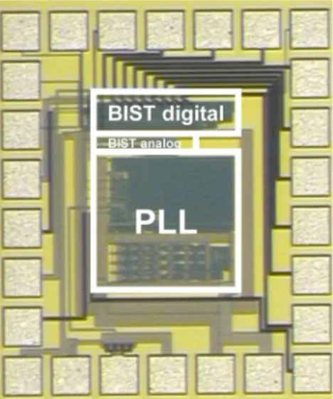
The measurement resolution kRES of TDC in (6) must be calibrated. Using the clock period Toof VCO as the reference yields an accurate pulsewidth to calibrate the TDC. The DIV is modified to yield a pulsewidth that equals the clock period of the VCO. As shown in Fig. 11, a logic gate and a retiming latch are added to change the duty cycle of the output signal of the DIV.
Fig. 12 shows the calibration circuit of the BIST. The DIV output is connected to CP2 via MUX. In the calibration mode, the control signal MUXSEL changes to a logic high to allow the DIV output signal to pass through the MUX. The pulse signal is input to CP2 and changes the voltage of the loop filter and the frequency of the VCO. The pulsewidth T0is the clock period of the VCO, and the count NCALof the counter can be obtained. The pulsewidth is related to the count as
T0= kRES(NCAL− N0) (9) where N0is the count of the counter if the DIV frequency does not deviate from the original frequency.
The clock period T0 of the VCO varies. It is known as the period jitter. Repeating the calibration process a particular number of times produces a histogram of different NCAL. The average clock period T0equals the period of the reference clock
Fig. 10. Timing diagram of control unit.
Fig. 11. DIV with an output pulsewidth that equals the period of VCO.
Fig. 12. Calibration circuit.
divided by N . The measurement resolution can be calibrated using the equation
kRES=
T0
NCAL− N0
(10)
where NCALis the average value of NCAL.
The purpose of adding DL2 to the calibration circuit is to delay the DIV output signal CLK1 for a clock period of the VCO or some longer time to maintain the pulsewidth of the DIV output after the VCO frequency is changed. Fig. 13 shows the timing diagram of the calibration. The pulsewidth W1 equals the clock period of the VCO before the frequency is changed.
W2 is the clock period of the VCO after the frequency is changed. The DL2 successfully maintains the pulsewidth of the CLK1 at W1.
Fig. 13. Timing behavior of calibration.
IV. EXPERIMENTALRESULTS
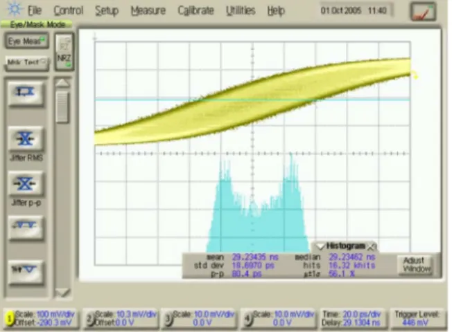
Figs. 14 and 15 show the chip photograph and the measure-ment equipmeasure-ment, respectively. The chip is implemeasure-mented using a 0.18-µm CMOS technology. The BIST circuit includes the digital and analog parts. The power supplies are separated to
Fig. 14. Chip photograph.
Fig. 15. Measurement equipment.
Fig. 16. Injecting noise into the power line.
prevent the disturbance of the noise from the digital circuit. The DIV output clock signal is measured using an oscilloscope, and the BIST output digital signal is measured using a logic analyzer. The noise that is injected for measurement is produced using a function/arbitrary waveform generator.
As shown in Fig. 16, the noise of various amplitudes and forms is injected into the power line on the PCB through a coupling C to measure the BIST performance in various environments. The power line on the PCB can be modeled as an ideal power source in series with a parasitic resistor. The combination of the coupling C and the parasitic resistor constitutes a high-pass filter. A high-frequency noise is injected to the tested chip, whereas a low-frequency noise is filtered out. The coupling C is designed to be as large as possible to allow
Fig. 17. PLL DIV output clock jitter with 40-mV p-p random noise.
Fig. 18. Histogram of the BIST output in calibration mode with 40-mV p-p random noise.
more noise to pass through. In this paper, a 10-µF coupling C is used.
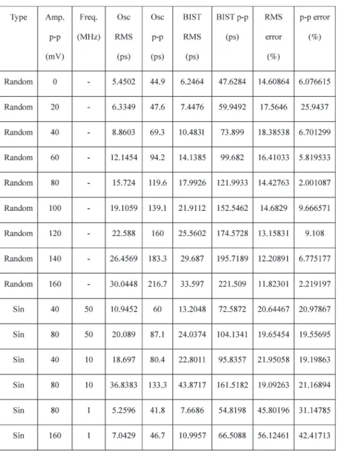
The operating frequency of the PLL is 1.25 GHz. The refer-ence clock and the feedback clock are operated at 78.125 MHz. Fig. 17 shows the PLL feedback-clock waveform measured using an oscilloscope and the jitter histogram of 16-k hits. A 40-mV peak-to-peak (p-p) random noise is injected into the power line. The measured rms jitter and the p-p jitter are 8.8603 and 69.3 ps, respectively.
Fig. 18 shows the histogram of the BIST output in the calibration mode in the same environment that was previously described. In the calibration mode, the histogram of the output values of the BIST is that of the period jitter. According to (10), the average clock period of the VCO, which is 800 ps when the PLL is operated at 1.25 GHz, can be used to calibrate the measurement resolution. The counting time Nois designed to be 16 384 times the period of the reference clock. From the histogram of the BIST output, the average value NCALis calculated at 15 702. The coefficient kRES can be calculated using (10) as 800/(15 702− 16 384) = −1.1730 ps/count. The sign of the coefficient is negative because the gain of the VCO is negative in this design.
Fig. 19. Histogram of the BIST output in the test mode with 40-mV p-p random noise.
Fig. 20. PLL DIV output jitter measured using an oscilloscope with 40-mV p-p 10-MHz sinusoidal noise.
Fig. 19 shows the histogram of the BIST output in the test mode with a 40-mV p-p random noise. For comparison, the total number of the data samples measured to produce the histogram equals the number of the hits measured using an oscilloscope. Each output value of the BIST in the test mode represents the phase difference between the reference clock and the feedback clock, and the histogram of the BIST output values represents the histogram of the timing jitter. Since the measurement resolution kRES in (6) was calibrated, the jitter magnitude can be determined by simply multiplying the output values of the BIST output data by the measurement resolution. The p-p jitter and the rms jitter of the PLL in this case are
|−1.1730| ∗ (15 940 − 15 877) = 73.899 ps and |−1.1730| ∗
8.937 = 10.4831 ps, respectively.
Figs. 20–22 show the histograms measured using an oscillo-scope, the BIST in the calibration mode, and the BIST in the test mode, respectively, when the power line is injected with a 40-mV 10-MHz sinusoidal noise. The rms jitter and the p-p jitter measured using an oscilloscope are 18.6970 and 80.4 ps, respectively. The rms jitter and the p-p jitter measured using the BIST are 22.8011 and 95.8357 ps, respectively. Since the noise is sinusoidal, the histograms of the period jitter and the timing jitter have two peaks, as expected.
Fig. 21. Histogram of the BIST output in the calibration mode with 40-mV p-p 10-MHz sinusoidal noise.
Fig. 22. Histogram of the BIST output data in the test mode with 40-mV p-p 10-MHz sinusoidal noise.
Table I presents more cases. Figs. 23 and 24 compare the p-p jitter and the rms jitter measured using an oscilloscope and a BIST circuit. The measurement errors in most of the cases are under 20%, except in the case with a 1-MHz noise. As mentioned in Section II, the TDC utilizes the VCO and loop filter of the PLL under test as parts of the circuit, but the initial value of the VCO control voltage is not constant due to supply noise and PLL-tracking ability. This is believed to be the main cause of the measurement error in the experimental result.
Tables II and III summarize this work. The area overhead is 36.7%. The supply voltage is set to 1.85 V because the BIST circuit does not function when the voltage is under 1.85 V. The problem has not been solved. However, the problem may probably arise in the analog circuit of the BIST because the digital circuit is insensitive to the power-supply voltage.
The measurement time of 3.44 s is too long for the test appli-cation. To improve the performance, a high-speed counter such as the ripple counter could directly be connected to the VCO for frequency measurement. It could shorten the measurement time to about one-tenth or less. The multiphase phase detector [15] could also be applied to further shorten the measurement time to less than one-hundredth of this paper.
TABLE III BIST SPECIFICATIONS
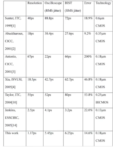
Table IV compares the results herein with those reported elsewhere. This paper has a resolution of 1.17 ps, which is the finest as compared with those using the same or even better technologies. The measurement error is relatively small (14.6%) and acceptable for the test application.
V. CONCLUSION
A BIST circuit to measure the CP-PLL jitter is presented. When the loop filter and the VCO of the PLL under test are utilized as parts of the BIST circuit, the area overhead is small. The resolution can be as high as subpicoseconds or even higher at the expense of the measuring time. The chip is fabricated using a 0.18-µm CMOS technology; the BIST
circuit is run at 78.125 MHz, and the VCO of the PLL is run at 1.25 GHz. The measurement results show a resolution of 1.17 ps, a measurement error of 14.6%, and an area overhead of 36.7%.
ACKNOWLEDGMENT
The authors would like to thank the National Chip Imple-mentation Center (CIC) for the chip fabrication.
REFERENCES
[1] S. Sunter and A. Roy, “BIST for phase-locked loops in digital applica-tion,” in Proc. ITC, 1999, pp. 532–540.
[2] N. Abaskharoun and G. W. Roberts, “Circuits for on-chip sub-nanosecond signal capture and characterization,” in Proc. IEEE Custom Integr.
Cir-cuits Conf., 2001, pp. 251–254.
[3] A. H. Chan and G. W. Roberts, “A deep sub-micron timing measurement circuit using a single-stage Vernier delay line,” in Proc. IEEE Custom
Integr. Circuits Conf., 2002, pp. 77–80.
[4] T. Xia, H. Zheng, J. Li, and A. Ginawi, “Self-refereed on-chip jitter measurement circuit using Vernier oscillators,” in Proc. IEEE Comput.
Soc. Annu. Symp. VLSI, 2005, pp. 218–223.
[5] K.-H. Chen, S.-Y. Jiang, and Z.-S. Chen, “BIST for clock jitter measure-ments,” in Proc. Int. Symp. Circuits Syst., 2003, pp. 577–580.
[6] C.-C. Tsai and C.-L. Lee, “An on-chip jitter measurement circuit for the PLL,” in Proc. Asian Test Symp., 2003, pp. 332–335.
[7] J.-J. Huang and J.-L. Huang, “A low-cost jitter measurement technique for BIST applications,” in Proc. Asian Test Symp., 2003, pp. 336–339.
surement,” IEEE Trans. Instrum. Meas., vol. 52, no. 6, pp. 1738–1748, Dec. 2003.
[14] K. A. Jenkins, A. P. Jose, and D. F. Heidel, “An on-chip jitter measurement circuit with sub-picosecond resolution,” in Proc. Eur. Solid-State Circuits
Conf., 2005, pp. 157–160.
[15] M. Chou, J. Hsu, and C. Su, “A digital BIST methodology for spread spectrum clock generators,” in Proc. Asian Test Symp., 2006, pp. 251–254.
electrical and computer engineering from the Univer-sity of Wisconsin at Madison, in 1990.
Since graduation, he has been with the Depart-ment of Electrical and Control Engineering, National Chiao Tung University. His research interests are in the areas of mixed-analog and digital-system testing and design for testability. He is also involved in projects on baseband and circuit design for wireless communication.