Analysis of Ga As Ga Sb Ga As structures under optical excitation considering
surface states as an electron reservoir
Hong-Wen Hsieh and Shun-Tung Yen
Citation: Journal of Applied Physics 105, 103515 (2009); doi: 10.1063/1.3129616
View online: http://dx.doi.org/10.1063/1.3129616
View Table of Contents: http://scitation.aip.org/content/aip/journal/jap/105/10?ver=pdfcov Published by the AIP Publishing
Articles you may be interested in
Fermi level shift in Ga In N As Sb Ga As quantum wells upon annealing studied by contactless electroreflectance
Appl. Phys. Lett. 90, 061902 (2007); 10.1063/1.2437729
Thermal quenching mechanism of photoluminescence in 1.55 m Ga In N As Sb Ga ( N ) As quantum-well structures
Appl. Phys. Lett. 89, 101909 (2006); 10.1063/1.2345240
Nonlinear optical transitions of Ga As Al Ga As asymmetric double-well structures Appl. Phys. Lett. 89, 032114 (2006); 10.1063/1.2220533
Surface and interface barriers of In x Ga 1x As binary and ternary alloys J. Vac. Sci. Technol. B 21, 1915 (2003); 10.1116/1.1588646
Surface and interface properties of In 0.8 Ga 0.2 As metal–insulator–semiconductor structures J. Vac. Sci. Technol. B 20, 1759 (2002); 10.1116/1.1491537
Analysis of GaAs/ GaSb/ GaAs structures under optical excitation
considering surface states as an electron reservoir
Hong-Wen Hsieh and Shun-Tung Yena兲
Department of Electronics Engineering, National Chiao Tung University, 1001 Ta-Hsueh Road, Hsinchu, Taiwan 30050, Republic of China
共Received 27 February 2009; accepted 8 April 2009; published online 22 May 2009兲
We present a self-consistent model for the analysis of the carrier distribution, the band profile, and the transition energy of type-II aligned GaAs/GaSb/GaAs structures under optical excitation. The model considers the surface states as an electron reservoir, associated with pinning of the conduction band Fermi level at the midgap. In our model, the optical generated holes in the GaSb quantum well causes a potential well on one side of the GaSb layer, which can efficiently accommodate the optically generated electrons. Accordingly, we derive a relation connecting the excitation power to the carrier density. Using the relation and the effective triangular potential approximation, we obtain a simple formula for the transition energy shift as a function of the excitation power, which follows the cube-root rule quite well. The calculation allows the determination of the band offset of a type-II heterointerface by comparison with data from photoluminescence measurement. The result suggests the unstrained valence band offset of GaSb/GaAs to lie between 0.5 and 0.55 eV. We also present a simplified model for analyzing the electronic and optical properties of type-II heterostructures without the need of a self-consistent calculation. © 2009 American Institute of Physics. 关DOI:10.1063/1.3129616兴
I. INTRODUCTION
The GaSb/GaAs heterostructures have received much attention because of their peculiar type-II band alignment that can cause interesting electrical and optical properties. The state-of-the-art epitaxy technology has permitted growth of high-quality GaSb quantum wells 共QWs兲 and self-assembled quantum dots embedded in the GaAs matrix.1–5 However, until now there still lacks a compelling unambigu-ous figuration for the band alignment. The difficulty in de-termining the band offset arises from the abnormal band pro-file of the highly strained GaSb/GaAs structure which may be influenced by external pumping in photoluminescence 共PL兲 measurement. It therefore requires an appropriate model along with an ingenious experimental arrangement to explore the detail about the band profile.
There have been a few studies attempting to figure out the electronic structure of the GaSb/GaAs QW.1–8Ledentsov
et al.2made a theoretical calculation of PL peak energy for the GaSb/GaAs structure but found a large discrepancy. Lo
et al.3attributed the discrepancy to the choice of an incorrect valence band offset 共VBO兲 and estimated the unstrained VBO for the GaSb/GaAs alignment to be about 0.4 eV from their PL measurement and theoretical calculation. Qteish and Needs6 used self-consistent pseudopotential techniques to determine the band offset. They found a strained VBO of 1.1 eV, corresponding to a high unstrained VBO of 0.88 eV. Nakai and Yamaguchi7predicted an even higher VBO value from the PL transition energy for 1 monolayer 共ML兲 GaSb/GaAs QW structures. All the aforementioned studies did not take into account seriously the effect of carrier accu-mulation which is important in the type-II QW structure. It
needs a calculation with the Schrödinger and the Poisson equations solved self-consistently. Liu et al.8considered the carrier accummulation and estimated the unstrained VBO to be about 0.6 eV by fitting their calculation to the experimen-tal data for GaAsSb/GaAs QWs. However, the surface con-dition, which can significantly influence the band profile for the samples grown with the GaSb layer near the surface, has not yet been imposed properly on the calculations.
In this paper we demonstrate a self-consistent model that considers the surface states as a reservoir of electrons asso-ciated with pinning of the conduction band Fermi level at the midgap.9,10 By this model, we analyze the charge distribu-tion, the band profile, and the transition energy for GaAs/GaSb/GaAs structures under optical excitation. The resulting band profile and carrier distribution are different in character from those by the conventional symmetric band model.2,3,8Based on the configuration of carrier distribution, we derive a relation connecting the excitation power to the carrier density and also a relation of the transition energy shift versus the excitation power. Our model accompanied with experimental data from PL measurement is then used to determine the unstrained VBO of GaSb/GaAs. We also give a simplified version of the model that needs no self-consistent calculation. It will be useful and convenient for analyzing experimental data.
This paper is organized as follows. In Sec. II, we will describe the self-consistent model. Formulas connecting the calculation to the PL measurement will be derived in Sec. III. We will then use our theoretical model to determine the VBO of GaSb/GaAs by comparison with the measured data in Sec. IV. A simplified model and discussion with respect to it will be given in Sec. V. Finally, we draw a conclusion in Sec. VI.
a兲Electronic mail: [email protected].
0021-8979/2009/105共10兲/103515/7/$25.00 105, 103515-1 © 2009 American Institute of Physics
II. SELF-CONSISTENT MODEL
We consider GaAs/GaSb/GaAs QW structures, as an example, which are basically the same as those in Ref. 3. They were formed with a thin GaSb layer sandwiched be-tween two 150 nm GaAs epilayers 共nominally undoped, the acceptor concentration is Na⬇1015cm−3兲, grown on the 共100兲 n-type GaAs substrate 共the donor concentration is Nd ⬇1018cm−3兲. In the samples there was an additional GaSb surface submonolayer共⬇0.5 ML兲 grown on the GaAs cap-ping layer to check the thickness of the GaSb QW. In the present work, we neglect this surface layer because it will not influence significantly our calculation. Almost all the pa-rameters in our calculation are adopted from Ref. 11. The unstrained VBO of GaSb/GaAs is set at 0.55 eV for the moment.
It is instructive first to consider the case at thermal equi-librium. In the present study, the surface states of GaAs serve as a high density-of-states reservoir of electrons such that the Fermi level can be assumed to be pinned at the midgap. At the interface between the GaAs epilayer and the GaAs sub-strate, the Fermi level is near the conduction band edge be-cause of the heavily doping of the n-type substrate. As a result, the band profile of the GaAs/GaSb/GaAs structure can simply be drawn as shown in Fig. 1, where the GaSb QW is just inserted at the midpoint of a 300 nm GaAs layer subjected to a uniform internally built-in electric field F0 = Eg/2ed 共here Egis the band gap of GaAs, e is the elemen-tary charge, and d = 300 nm is the sum of the lengths of the GaAs epilayers兲. Detailed calculation considering the charge distribution in each of the layers results in an indistinguish-able band profile for the samples since the charge density other than at the two end boundaries is negligibly small. The simple picture in Fig. 1 also reveals that there are excess electrons trapped by the surface states and balanced positive charge of ionized donors at the interface between the GaAs epilayer and the n-GaAs substrate. The excess electron den-sity at the surface can easily be estimated to be ns0=⑀F0/e = 1.85⫻1011cm−2, where⑀is the permittivity of GaAs.
Also shown in the figure are the envelope functionhof the first valence subband edge state of the GaSb/GaAs QW
and the one c of a quasibound conduction subband edge state confined to the left of the GaSb barrier. The valence subband states have a lifetime much longer than that of any observable electronic process so as to be regarded as local-ized states. On the other hand, the lifetime of the quasibound conduction subband states is as short as of the order of 10−12s for a 2 ML GaSb barrier, estimated by the approach in Ref. 12. This implies that under extremely weak optical excitation, the optically generated holes can be captured and populate into the QW but the electrons cannot accumulate around the GaSb barrier. With increasing optical pumping power, more electron-hole pairs are generated and then more electrons共holes兲 are trapped at the surface 共QW兲 states, lead-ing to a higher built-in electric field FLin region L which is the region of the GaAs layer to the left of the GaSb layer and screening the electric field in region R which is the region of the GaAs layer to the right of the GaSb layer.
For the pumping power I above a critical value Icr, the band profile is such that there appears a localized conduction subband in region R, as illustrated in Fig.2, and hence, elec-trons can accumulate around the GaSb barrier. It is obvious that for samples subjected to the critical power excitation, the band profile of region R is approximately flat and the electric field in region L is about 2F0共i.e., twice the field at thermal equilibrium兲. Accordingly, the surface charge density at the critical condition ns,cris about 2ns0共=3.7⫻1011 cm−2兲. Further increasing the pumping power when I⬎Icr can sig-nificantly increase the electron concentration n in region R but cause only a slight increase in the percentage of the hole concentration p in the QW because there has existed a con-siderable hole concentration in the QW at the critical condi-tion I = Icr. Because of the efficient accumulation of electrons in region R, the electric field FLin region L is expected to be insensitive to the pumping power above the critical
condi-0 50 100 150 200 250 300 -2.0 -1.6 -1.2 -0.8 -0.4 0.0 0.4 0.8 1.2 Energy (eV ) z (nm) Ec Ev Region L Region R ϕe ϕh
FIG. 1.共Color online兲 The band diagram of the GaAs/GaSb/GaAs structure grown on n-type substrate at thermal equilibrium. The diagram is obtained by letting the Fermi level at the surface be pinned at the midgap. The blue dashed line shows the envelope function of the conduction subband, e, which is leaky in character. The red dotted line shows the envelope function of the valence subband,h, which is localized in character.
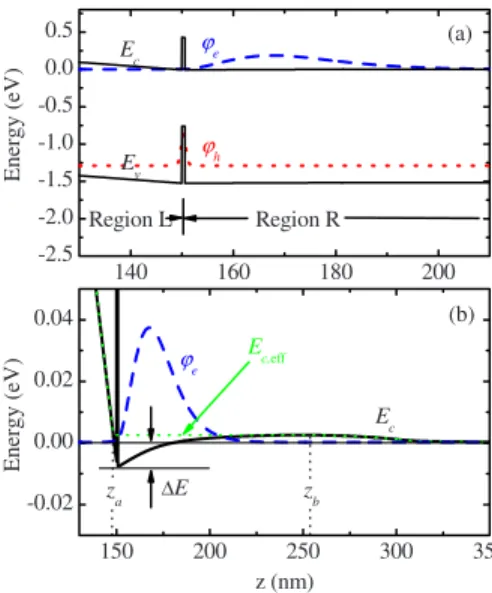
150 200 250 300 350 -0.02 0.00 0.02 0.04 140 160 180 200 -2.5 -2.0 -1.5 -1.0 -0.5 0.0 0.5 zb Ec (b) ϕe E nergy (e V) z (nm) Ec,eff za ∆E Region L Region R Ev Ec ϕh ϕe Energy (eV ) (a)
FIG. 2. 共Color online兲 共a兲 The band diagram of the GaAs/GaSb/GaAs structure under sufficient optical excitation共I⬎Icr兲. There appears a local-ized conduction subband on the right side of the GaSb barrier, whose enve-lope functioneis shown by the blue dashed line. The band diagram and the envelope functions are obtained by the self-consistent calculation.共b兲 Zoom in for the conduction band profile and the envelope function around the GaSb barrier. Also shown is the profile of Ec,eff, which is used for calculating the three-dimensional density of states.
103515-2 H.-W. Hsieh and S.-T. Yen J. Appl. Phys. 105, 103515共2009兲
tion; otherwise, a significant increase in FLwould imply an enhanced accumulation of electrons in region R, which con-versely reduces FL.
Based on the above arguments without complicated cal-culation, we conclude that only when I⬎Icrcan significant PL involving GaSb/GaAs QW states be observed. Also we can make reasonable assumptions for our self-consistent cal-culation scheme appropriate to the PL experiment. In our model, the conduction and the valence band profiles are given by
Ec共z兲 = Ec0共z兲 − e⌽共z兲,
Ev共z兲 = Ev0共z兲 − e⌽共z兲, 共1兲
respectively, where Ec0and Ev0are the flat band profiles of the conduction and the valence bands, respectively, and⌽ is the electric potential which is the solution of the Poisson equation, d dz⑀ d dz⌽ = − e共p − n + Nd + − Na −兲. 共2兲
Here,⑀is the electric permittivity, and p, n, Nd+, and Na−are the densities of holes, electrons, ionized donors, and ionized acceptors, respectively. The Nd+and Na−are given by
Nd + = Nd 1 + 2e共EFc−Ed兲/kBT, Na−= Na 1 + 4e共Ea−EFv兲/kBT, 共3兲
where Ed共Ea兲 is the donor 共acceptor兲 level, EFc共EFv兲 is the quasi-Fermi level of the conduction共valence兲 band, kBis the Boltzmann constant, and T is the temperature. We set the doping concentrations at zero for the epilayers. For the hole concentration p, we consider only the holes occupying the first subband in the QW and take the parabolic band approxi-mation, giving
p =兩h兩2pw, 共4兲
where pw is the sheet concentration of holes 共in cm−2兲 ex-pressed by
pw= kBTmh
ប2 ln关1 + e共Eh−EFv兲/kB
T兴, 共5兲
with mhas the hole effective mass and Ehas the level of the first valence subband edge. The approximation is applicable to the case of a narrow QW under low excitation at low temperature. For the electron concentration n, we use
n =兩e兩2nw+ 2
冉
kBTme 2ប2冊
3/2 F1/2冉
EFc− Ec,eff kBT冊
, 共6兲where the first term accounts for the electrons occupying the first conduction subband and the second term accounts for the residual electrons that are free from the quantization con-finement. nw is the sheet concentration of electrons in the first subband expressed by
nw= kBTme
ប2 ln关1 + e共EFc
−Ee兲/kBT兴, 共7兲
with meas the electron effective mass and Eeas the level of the first conduction subband edge. The omission of other subbands is because of their absence in the shallow QW, as will be the case in the present study. In the second term in Eq. 共6兲, F1/2 is the Fermi integral and Ec,eff is the profile of the effective conduction band edge for the three-dimensional density of states, g3D共E兲␣
冑
E − Ec,eff共with E as the energy兲. A reasonable Ec,effprofile is set as关see Fig.2共b兲兴Ec,eff共z兲
=
再
Ec共zb兲, za⬍ z ⬍ zb共z in the region of the well兲Ec共z兲, otherwise,
冎
共8兲 where zbis the position at which Ec共z兲 has a local maximum in region R and zais the position at which Ec共za兲=Ec共zb兲 in region L. It is noticed that the isotropic parabolic band ap-proximation is taken only for the simple formulas of carrier concentrations but not for calculating the envelope functions and the levels of the subband edge states. The envelope func-tions h and e associated with their energies Eh and Ee, respectively, are calculated by the eight-band k · p model.13 The quasi-Fermi level EFcof the conduction band is assumed to be flat共and set as the energy reference兲 because there is no applied voltage bias and the thickness of the structure is small compared to the electron diffusion length. The Poisson equation 共2兲 is solved under the Dirichlet boundary condi-tion: at the surface, the EFcis assumed pinned at the midgap and at the other boundary, which is set at a place deep enough inside the substrate, the conduction band edge Ec relative to EFc is determined by the doping concentration Nd= 1018 cm−3.
A self-consistent calculation with the Schrödinger and the Poisson equations is then performed for the band profile and the carrier distributions. The charge neutrality of the whole structure is ensured by the flatness of the band inside the substrate. In the calculation, the value of the hole effec-tive mass mhof strained GaSb is given by Ref.6and all the other parameters used in the calculation are given by Ref.11. The temperature is set at T = 15 K for comparision with the experiment in Ref. 3.
Now that only the holes occupying the first subband are considered, it is convenient to use the sheet density of the holes pwas the input parameter in calculating the band pro-file and carrier distributions. We find that the localized con-duction subband appears only when pwis greater than a crital value pcr, which is found to be 3.8⫻1011cm−2. For pw ⬍pcr, the calculation based on formulas共1兲–共8兲cannot con-verge. For pcr⬍pw⬍4.5⫻1011cm−1, we find that the built-in electric field in region L is almost fixed and the sur-face excess electron density ns is nearly fixed at 3.75
⫻1011cm−2, which is slightly higher than
2ns0共=3.7⫻1011cm−2兲 and slightly lower than pcr. The in-crease in pwcauses only the increase in n in region R. Figure 3 shows the sheet density of the subband electrons, nw, and the difference pw− ns as functions of pw. The range of pwin
the figure corresponds to the consequence that the differ-ences, EFc− Ee and Eh− EFv, do not exceed several meV, in accordance with our low excitation assumption. As can be seen, both nw and pw− ns curves are linear and parallel to each other. Accordingly, we can write
nw= pw− ns− Nres, 共9兲
where Nres= 6⫻109cm−2 is the sheet density accounting for the residual charge other than the charges of pw, nw, and ns. Similar to ns, the Nresis almost independent of pw. The re-sults and argument so far are basically independent of the thickness of the GaSb layer.
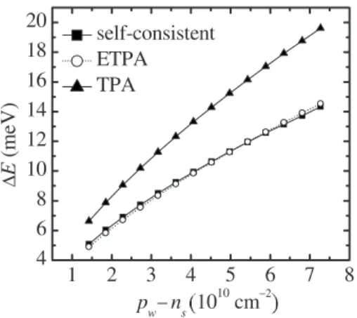
The simultaneous increase in pwand nwwill cause deep-ening of the electron QW and shifting of the conduction subband edge. Figure4shows⌬E共⬅Ee− Ec,min兲, which is the conduction subband edge Eemeasured from the minimum of Ec 共denoted by Ec,min兲 as indicated in Fig. 2共b兲, versus pw − ns, obtained by three different calculations. The triangular potential approximation共TPA兲 is conventionally used to es-timate⌬E. In TPA, the ⌬E can be expressed by
⌬E = 2.388
冉
ប2F2 2me冊
1/3
, 共10兲
which is obtained using an infinite triangular potential profile of a uniform electric field F to replace the realistic potential profile in region R. For
F =e
⑀共pw− ns兲, 共11兲
which is the electric field at the bottom of the realistic QW, we find a significant overestimate of ⌬E obtained by TPA compared to the result obtained by our self-consistent calcu-lation, as shown in Fig. 4. The deviation is enhanced with
pw− ns increasing. It can be considerably eliminated by the effective triangular potential approximation共ETPA兲 that uses an average electric field
F =e
⑀共pw− ns兲, 共12兲
where is in the range of 0⬍⬍1 and to be used as a fitting parameter. We find that the⌬E obtained by ETPA with
= 0.638 almost coincides with the result by the self-consisent calculation in the range of pw− ns from 1 ⫻1010to 7⫻1010cm−2 The ETPA will be useful in later analysis and is also popular in device modeling.14
III. CONNECTION OF CALCULATION TO EXPERIMENT To connect the theoretical calculation to the PL experi-ment, it is required to have a relation between the excitation power I and the hole density pwfor samples in a steady state. Under the steady state condition, the excitation of carriers is balanced by the recombination of carriers. Ledentsov et al.2 gave a simple relation based on a symmetric band model in which the electron and the hole sheet densities are equal,
nw= pw, in the neighborhood of the GaSb layer. As a result,
I =␣pwnw=␣pw2, 共13兲
where the coefficient␣can be obtained by fitting to experi-mental data.2 With relation 共13兲,⌬E can be expressed as a function of I by the ETPA with F =epw/2⑀,
⌬E = 1.194
冉
ប22e2me⑀2␣
冊
1/3I1/3. 共14兲
This is the famous cube-root relation between the energy shift and the excitation power.2–5Relation共14兲allows one to determine␣ by PL measurement of the relation of the tran-sition energy Ee− Eh versus I since⌬E is equal to the tran-sition energy minus the separation Ec,min− Eh, which is al-most independent of I. We can then obtain the optically generated hole density pwas a function of excitation power I by Eq. 共13兲.
The situation is more complicated for the pw-I and the ⌬E-I relations appropriate to our model. To derive the rela-tions, we notice that the carrier recombination process occurs primarily not only in the neighborhood of the QW but also at the surface. Since the surface states is assumed to be an electron reservoir associated with pinning of the Fermi level at the midgap, the surface recombination rate is totally deter-mined by the flow of optically generated holes toward the surface in region L. The hole current is proportional to the product of the driving electric field FL and the hole density. For I⬎Icr 共pw⬎pcr兲, as has described previously, FL is nearly independent of pw 共and thus of I兲. Since the hole generation rate is proportional to I, the surface recombination
3.8 4.0 4.2 4.4 4.6 2 4 6 8 concentration
(
10 10 cm −2)
pw(
1011cm−2)
nw pw−nsFIG. 3. The relation of pw− nsvs pwand that of nwvs pw.
1 2 3 4 5 6 7 8 4 6 8 10 12 14 16 18 20 ∆ E (meV ) pw−ns
(
1010cm−2)
self-consistent ETPA TPAFIG. 4. The energy difference⌬E as a function of pw− ns by three
ap-proaches: the self-consistent calculation, the ETPA, and the TPA. For ETPA, we use= 0.638.
103515-4 H.-W. Hsieh and S.-T. Yen J. Appl. Phys. 105, 103515共2009兲
rate should also be proportional to I. Also, since the total recombination rate is proportional to I in steady state, we conclude that the rate of radiative recombination occuring around the QW is proportional to I. Consequently, consider-ing the optical transition from the conduction to the valence subbands, we can write
I⬀ 兩具h兩e典兩2pwnw. 共15兲 The factor 兩具h兩e典兩2 is important in the expression because it increases with I increasing that causes deepening of the electron QW and enhances the overlap of wavefunctions. In fact, from our self-consistent calculation, we find that
兩具h兩e典兩2⬀ pw− ns 共16兲
for pcr⬍pw⬍5⫻1011cm−2. Using Eqs.共16兲and共9兲for nw, we can rewrite Eq.共15兲as
I =共pw− ns兲2pw
冉
1 − Nrespw− ns
冊
, 共17兲
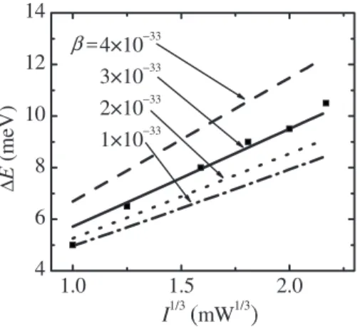
where  is a coefficient that can be determined by experi-ment. Relation 共17兲with the ETPA关Eqs.共10兲 and共12兲兴 al-lows us to calculate the energy shift ⌬E versus I if  is known. Figure5shows the curves of⌬E versus I1/3obtained by our calculation with  as a parameter, and also the ex-perimental data from Ref.3. Strikingly, the cube-root rule for the ⌬E-I relation is applied quite well to the present case. This can be understood by writing⌬E in the form
⌬E = 2.388
冉
ប22e2 2me⑀2ns冊
1/3
I1/3f , 共18兲
where the factor f, defined as
f =
冢
ns/pw 1 − Nres pw− ns冣
1/3 , 共19兲changes slightly with the excitation power since the ns and the Nreskeep almost constant and the pwchanges only within a small range. For ns= 3.75⫻1011 cm−2, Nres= 6⫻109cm−2,
f varies from 1.17 to 1.03 as pw changes from 3.9 ⫻1011to 4.1⫻1011cm−2, corresponding to I changing from 1 to 10 mW, as will be seen in Fig.6.
The PL measurement cannot give the absolute value of ⌬E, as defined in Fig.2共b兲, but the variation in the transition energy with I. In Fig.5, we plot the experimental data from Ref. 3 totally by shifting a common energy. The slope of the ⌬E-I1/3 line best fit to the experimental data, which is 4.38 meV/mW1/3, suggests the coefficient = 2 ⫻10−33mW cm6.
With the known, we can calculate the hole concentra-tion pwas a function of I using Eq.共17兲. Figure6shows the pwversus I obtained by our model using Eq.共17兲as well as that by the symmetric band model using Eq. 共13兲. As ex-pected, pw for our model changes slightly from 3.9 ⫻1011to 4.1⫻1011cm−2, within a range of 5%, with I changing from 1 to 10 mW, while for the symmetric band model, it changes considerably in percentage. It is only the electron concentration nw共or pw− ns兲 that varies significantly with I in our model.
IV. VBO DETERMINATION
To determine the VBO of GaSb/GaAs, we compare with the PL measurements3in Fig.7 the calculated transition en-ergies Ee− Eh for different thicknesses dwof the GaSb layer with the unstrained VBO as a parameter. The data in the
1.0 1.5 2.0 4 6 8 10 12 14 ∆ E (meV ) I1/3
(
mW1/3)
β=4×10⁻³³ 3×10⁻³³ 2×10⁻³³ 1×10⁻³³FIG. 5. The calculated energy difference⌬E as a function of the cube root of excitation power, I1/3, withas a parameter共in mW·cm6兲. Also shown are the experimental data共denoted by the filled squares兲 which are obtained by shifting the data of Ref.3by a common energy for the structure with a 2 ML GaSb layer. They give a slope d⌬E/dI1/3⬇4.1 meV/mW1/3, corre-sponding to⬇2⫻10−33mW· cm6. 0 2 4 6 8 10 1.2 1.8 2.4 3.0 3.6 4.2 4.8 pw×10 by Eq. (13) concentration
(
10 11 cm −2)
I (mW) pwby Eq. (17)FIG. 6.共Color online兲 The sheet concentration of holes pwvs the excitation
power I obtained by Eqs.共13兲and共17兲.
1 2 3 1.10 1.15 1.20 1.25 1.30 1.35 1.40 1.45 Trans iti on Energy (eV) GaSb Thickness (ML) 0.50 0.55 0.60 0.65 VBO=
FIG. 7.共Color online兲 Comparison of the calculated and the measured tran-sition energies vs the thickness of the GaSb layer. The calculated results are obtained with the unstrained VBO= 0.5, 0.55, 0.6, and 0.65.
figure correspond to an excitation power of 4 mW at which the hole concentrations pw are 4.15⫻1011 and 4.0 ⫻1011cm−2 for d
w= 1 and 2 ML, respectively, obtained by Eq. 共17兲. For dw= 3 ML, we cannot determine the corre-sponding value of pwdue to insufficient experimental infor-mation for determining . Fortunately, as has been implied by our model, the value of pw is basically insensitive to the GaSb layer thickness for a given I. We therefore assume pw to be 4.0⫻1011cm−2for d
w= 3 ML. The values of pwfor the three different dw are used as inputs in the self-consistent calculation to give the data in Fig. 7. The comparison in Fig. 7 suggests the unstrained VBO to lie between 0.5 and 0.55 eV, although the experimental and the calculated data for dw= 1 ML deviate from each other by about 0.03 eV 共about 2%兲. The slight inconsistency may result from the uncertainty in the thickness of the narrow epilayer due to the difficulty in growth and/or the exchange reaction of As and Sb atoms near the interfaces.
Lo et al.3 gave a similar determination of unstrained VBO but using the symmetric flat band model. Their calcu-lated transition energy is slightly lower than ours by a factor of ⌬E. As a result, Lo et al.3 obtained a lower unstrained VBO of 0.4 eV.
V. DISCUSSION AND SIMPLIFIED MODEL
We have demonstrated an analysis of the electronic properties of GaSb/GaAs heterostructures under optical ex-citation by a self-consistent model. It is worthy to discuss the usability of our model if some constraints are released. Firstly, if the EFcat the surface is assumed not necessarily to be pinned at the midgap but at a level EFcs below the con-duction band edge Ecsuch that there is a uniform internally built-in electric field F0and no localized subband in region L at thermal equilibrium, the electric field will be F0=共EFcs − Evs兲/ed associated with an excess electron density at the surface ns0=⑀F0/e, where Evsis the valence band edge at the surface. At the critical condition I = Icr, the electric field in region L is about FL=共EFcs− Evs兲/edL, the surface electron density is ns=⑀FL/e, and the hole density in the QW is pw = pcr, which is slightly larger than ns, where dL is the thick-ness of region L and unnecessary to be equal to the thickthick-ness of the epilayer in region R. For I⬎Icr, the FLand hence nsis assumed to be constant and pwslightly increases with I. The pw-I relation 共17兲 is still applicable and can reasonably be written as
pw= ns+
冑
Ins
. 共20兲
In deriving Eq. 共20兲, Nresin Eq. 共17兲is neglected and pwis replaced by ns for the case of low excitation and low tem-perature. The coefficientcan be determined by experiment using the formula
= 6.81ប 22e2 me⑀2ns
冉
d⌬E dI1/3冊
−1/3 , 共21兲which is obtained from Eq.共18兲by letting f = 1.
The above results and argument do not depend signifi-cantly on the thickness dwof the GaSb layer and the VBO of
GaSb/GaAs if the dwis small enough and the GaSb layer is an efficient barrier for electrons such that the ETPA is appli-cable. Moreover, they can also be applied to other type-II heterostructures.
The transition energy Ee− Eh is the sum of ⌬E and Ec,min− Eh. The separation Ec,min− Eh depends basically only on the QW width dwand the VBO but is nearly independent of the excitation power. On the other hand, ⌬E depends on the excitation power but is nearly independent of dw and VBO. These characters allow us to determine the VBO, as in Fig.7, without the need of a self-consistent calculation. We can use formula共18兲 with f = 1 for⌬E at a given I and the eight-band method for the relation between Ec,min− Eh and dw. Their sum then gives a relation between the transition energy and dw and can be used to determine the VBO by comparison with the measured transition energy. This simpli-fied model will be useful and convenient in analysis of the electronic and the optical properties of type-II heterostruc-tures.
VI. CONCLUSION
We have presented a self-consistent model that can be used to analyze the charge distribution, the band profile, and the interband transition energy for GaSb/GaAs type-II QW structures under optical excitation. The model considers the surface states as an electron reservoir such that the Fermi level of the conduction band is pinned at a fixed level. In the model, the accumulation of optically generated holes in the GaSb QW causes a GaAs QW on one side of the GaSb layer which can efficiently accommodate optically generated elec-trons, different from the case in the conventional symmetric band model. Based on the distribution of carriers, we have derived, considering the wavefunction overlap, a relation connecting the excitation power to the generated hole density in the QW. Using the relation and the effective triangular potential approximation, we have obtained a relation be-tween the shift of transition energy and the excitation power, which almost follows the cube-root rule. The derived formulas together with the data from PL measurement allow determining the band offset of a type-II aligned hetero-interface. The result suggests the unstrained VBO to lie between 0.5 and 0.55 eV. We have also given a simplified version of the model without the need of a self-consistent calculation. It will be useful and convenient for the analysis of experimental data.
ACKNOWLEDGMENTS
This work was supported by National Science Council of the Republic of China under Contract No. 97-2221-E-009-164.
1M. Yano, T. Iwawaki, H. Yokose, A. Kawaguchi, Y. Iwai, and M. Inouc,
Proc. SPIE1283, 221共1990兲.
2N. N. Ledentsov, J. Böhrer, M. Beer, F. Heinrichsdorff, M. Grundmann, D. Bimberg, S. V. Ivanov, B. Ya. Meltser, S. V. Shaposhnikov, I. N. Yassievich, N. N. Faleev, P. S. Kop’ev, and Zh. I. Alferov,Phys. Rev. B
52, 14508共1995兲.
3M. C. Lo, S. J. Huang, C. P. Lee, S. D. Lin, and S. T. Yen,Appl. Phys.
Lett.90, 243102共2007兲.
103515-6 H.-W. Hsieh and S.-T. Yen J. Appl. Phys. 105, 103515共2009兲
4F. Hatami, N. N. Ledentsov, M. Grundmann, J. Böhrer, F. Heinrichsdorff, M. Beer, D. Bimberg, S. S. Ruvimov, P. Werner, U. Gösele, J. Heydenreich, U. Richter, S. V. Ivanov, B. Ya. Meltser, P. S. Kop’ev, and Zh. I. Alferov,Appl. Phys. Lett.67, 656共1995兲.
5K. Matsuda, S. V. Nair, H. E. Ruda, Y. Sugimoto, T. Saiki, and K. Yamaguchi,Appl. Phys. Lett.90, 013101共2007兲.
6A. Qteish and R. J. Needs,Phys. Rev. B42, 3044共1990兲.
7T. Nakai and K. Yamaguchi,Jpn. J. Appl. Phys., Part 144, 3803共2005兲. 8G. Liu, S. L. Chuang, and S. H. Park,J. Appl. Phys.88, 5554共2000兲.
9J. Bardeen,Phys. Rev.71, 717共1947兲.
10P. E. Gregory, W. E. Spicer, S. Ciraci, and W. A. Harrison,Appl. Phys.
Lett.25, 511共1974兲.
11I. Vurgaftman, J. R. Meyer, and L. R. Ram-Mohan, J. Appl. Phys.89, 5815共2001兲.
12A. K. Ghatak, K. Thyagarajan, and M. R. Shenoy, IEEE J. Quantum
Electron.24, 1524共1988兲.
13A. Zakharova, S. T. Yen, and K. A. Chao,Phys. Rev. B66, 085312共2002兲. 14T. Janik and B. Majkusiak,IEEE Trans. Electron Devices45, 1263共1998兲.